
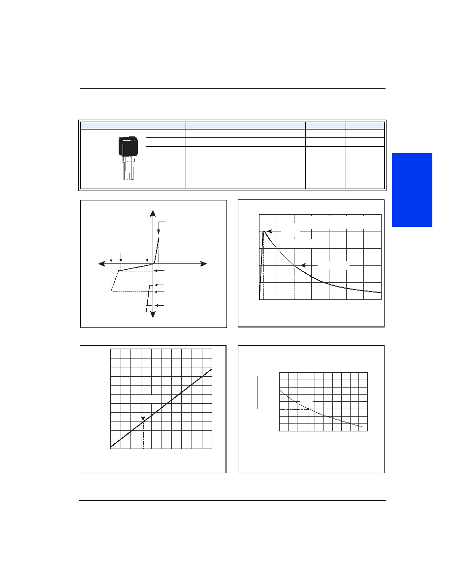
Twin SLIC Protector Modified TO-220
http://www.littelfuse.com
2 - 46
© 2004 Littelfuse, Inc.
+1 972-580-7777
SIDACtor
®
Data Book and Design Guide
Twin SLIC Protector Modified TO-220
Subscriber Line Interface Circuits (SLIC) are highly susceptible to transient voltages, such
as lightning and power cross conditions. To minimize this threat, Littelfuse provides this
dual-chip, fixed-voltage SLIC protector device.
For specific design criteria, see details in Figure 3.29.
* For surge ratings, see table below.
General Notes:
· All measurements are made at an ambient temperature of 25 °C. I
PP
applies to -40 °C through +85 °C temperature range.
· I
PP
is a repetitive surge rating and is guaranteed for the life of the product.
· V
DRM
is measured at I
DRM.
· V
S
and V
F
are measured at 100 V/µs.
· Special voltage (V
S
and V
DRM
) and holding current (I
H
) requirements are available upon request.
· Off-state capacitance (C
O
) is measured across pins 1-2 or 3-2 at 1 MHz with a 2 V bias. Capacitance across pins 1-3 is
approximately half.
· Parallel capacitive loads may affect electrical parameters.
· Compliance with GR 1089 or UL 60950 power cross tests may require special design considerations. Contact the factory for further
information.
Electrical Parameters
Part
Number *
V
DRM
Volts
V
S
Volts
V
T
Volts
V
F
Volts
I
DRM
µAmps
I
S
mAmps
I
T
Amps
I
H
mAmps
C
O
pF
Pins 1-2, 3-2
P0641A_2
58
77
4
5
5
800
2.2
120
40
P0721A_2
65
88
4
5
5
800
2.2
120
60
P0901A_2
75
98
4
5
5
800
2.2
120
60
P1101A_2
95
130
4
5
5
800
2.2
120
60
Surge Ratings (Preliminary Data)
Series
I
PP
2x10 µs
Amps
I
PP
8x20 µs
Amps
I
PP
10x160 µs
Amps
I
PP
10x560 µs
Amps
I
PP
10x1000 µs
Amps
I
TSM
60 Hz
Amps
di/dt
Amps/µs
A
150
150
90
50
45
20
500
C
500
400
200
150
100
50
500
1
3
2
(T)
(G)
(R)
Twin SLIC Protector Modified TO-220
© 2004 Littelfuse, Inc.
2 - 47
http://www.littelfuse.com
SIDACtor
®
Data Book and Design Guide
+1 972-580-7777
D
a
ta
S
h
e
e
ts
Thermal Considerations
Package
Symbol
Parameter
Value
Unit
Modified
TO-220
T
J
Operating Junction Temperature Range
-40 to +150
°C
T
S
Storage Temperature Range
-65 to +150
°C
R
JA
Thermal Resistance: Junction to Ambient
50
°C/W
PIN 1
PIN 2
PIN 3
I
H
I
T
I
S
I
DRM
V
DRM
V
T
+V
-V
+I
-I
V
S
I
H
I
DRM
V
DRM
V
T
+V
+I
V
S
I
S
I
T
V
F
-V
-I
V-I Characteristics
50
100
0
t
r
t
d
0
Peak
Value
Half Value
t Time (µs)
I
PP
P
eak Pulse Current %I
PP
t
r
= rise time to peak value
t
d
= decay time to half value
Waveform = t
r
x t
d
t
r
x t
d
Pulse Wave-form
-8
-40 -20
0
20 40 60 80 100 120 140 160
-6
-4
0
2
4
6
8
10
12
14
Junction Temperature (T
J
) °C
P
ercent of
V
S
Change %
25 °C
Normalized V
S
Change versus Junction Temperature
0.4
-40 -20
0
20 40 60 80 100 120 140 160
0.6
0.8
1.0
1.2
1.4
1.6
1.8
2.0
Case Temperature (T
C
) °C
Ratio of
I
H
I
H
(T
C
= 25 °C)
25 °C
Normalized DC Holding Current versus Case Temperature