LTC6910-2
1
69102i
, LTC and LT are registered trademarks of Linear Technology Corporation.
s
3-Bit Digital Gain Control (0, 1, 2, 4, 8, 16, 32
and 64V/V)
s
8-Pin TSOT-23 Package
s
Rail-to-Rail Input Range
s
Rail-to-Rail Output Swing
s
Single or Dual Supply: 2.7V to 10.5V Total
s
13MHz Gain Bandwidth Product
s
9nV/
Hz Input Noise at Gain of 64
s
120dB Total System Dynamic Range
s
Input Offset Voltage: 3mV (Gain = 1)
s
Input Offset Voltage: 2mV (Gain = 8)
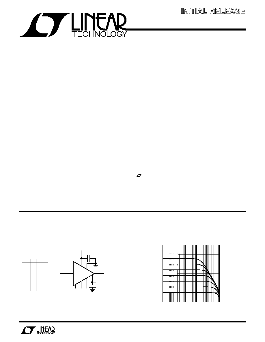
Digitally Controlled
Programmable
Gain Amplifier in SOT-23
April 2003
s
Data Acquisition Systems
s
Dynamic Gain Changing
s
Automatic Ranging Circuits
s
Automatic Gain Control
DESCRIPTIO
U
FEATURES
APPLICATIO S
U
TYPICAL APPLICATIO
U
Information furnished by Linear Technology Corporation is believed to be accurate and reliable.
However, no responsibility is assumed for its use. Linear Technology Corporation makes no represen-
tation that the interconnection of its circuits as described herein will not infringe on existing patent rights.
Final Electrical Specifications
The LTC
Ž
6910-2 is a low noise digitally programmable
gain amplifier (PGA) that is easy to use and occupies very
little PC board space. The gain is adjustable using a 3-bit
digital input to select inverting gains of 0, 1, 2, 4, 8, 16, 32
and 64V/V.
The LTC6910-2 is an inverting amplifier with a rail-to-rail
output. When operated with unity gain, the LTC6910-2
will also process rail-to-rail input signals. A half-supply
reference generated internally at the AGND pin supports
single power supply applications. Operating from single
or split supplies from 2.7V to 10.5V, the LTC6910-2 is
offered in an 8-lead TSOT-23 package.
For other gain options, see the LTC6910-1 and LTC6910-3.
2
1
3
V
IN
V
OUT
= GAIN ˇ V
IN
AGND
1
ľ
F OR LARGER
PIN 2 (AGND) PROVIDES BUILT-IN HALF-SUPPLY
REFERENCE WITH INTERNAL RESISTANCE OF 5k.
AGND CAN ALSO BE DRIVEN BY A SYSTEM ANALOG
GROUND REFERENCE NEAR HALF SUPPLY
69102 TA01
5
4
LTC6910-2
6
8
V
+
2.7V TO 10.5V
0.1
ľ
F
G2 G1 G0
7
G2
0
0
0
0
1
1
1
1
GAIN
0
1
2
4
8
16
32
64
G1
0
0
1
1
0
0
1
1
G0
0
1
0
1
0
1
0
1
Single Supply Programmable Amplifier
Frequency Response
FREQUENCY (Hz)
10
GAIN (dB)
30
50
0
20
40
100
1k
100k
1M
10M
69102 TA02
10
10k
V
S
=
ą
5V
V
IN
= 10mV
RMS
GAIN OF 64
GAIN OF 32
GAIN OF 16
GAIN OF 4
GAIN OF 8
GAIN OF 2
GAIN OF 1

LTC6910-2
2
69102i
Total Supply Voltage (V+ to V) ............................. 11V
Input Current .....................................................
ą
25mA
Operating Temperature Range (Note 2)
LTC6910-2C ....................................... 40
°
C to 85
°
C
LTC6910-2I ........................................ 40
°
C to 85
°
C
Specified Temperature Range (Note 3)
LTC6910-2C ....................................... 40
°
C to 85
°
C
LTC6910-2I ........................................ 40
°
C to 85
°
C
Storage Temperature Range ................. 65
°
C to 150
°
C
Lead Temperature (Soldering, 10 sec).................. 300
°
C
ORDER PART NUMBER
T
JMAX
= 150
°
C,
JA
= 230
°
C/W
LTC6910-2CTS8
LTC6910-2ITS8
(Note 1)
The
q
denotes the specifications that apply over the full operating
temperature range, otherwise specifications are at T
A
= 25
°
C. V
S
= 5V, AGND = 2.5V, Gain = 1 (Digital Inputs 001),
R
L
= 10k to midsupply point, unless otherwise noted.
PARAMETER
CONDITIONS
MIN
TYP
MAX
UNITS
Voltage Gain (Note 4)
V
S
= 2.7V, Gain = 1, R
L
= 10k
q
0.06
0
0.08
dB
V
S
= 2.7V, Gain = 1, R
L
= 500
q
0.1
0.02
0.06
dB
V
S
= 2.7V, Gain = 2, R
L
= 10k
q
5.96
6.02
6.10
dB
V
S
= 2.7V, Gain = 4, R
L
= 10k
q
11.9
12.02
12.12
dB
V
S
= 2.7V, Gain = 8, R
L
= 10k
q
17.80
17.98
18.15
dB
V
S
= 2.7V, Gain = 8, R
L
= 500
q
17.65
17.95
18.15
dB
V
S
= 2.7V, Gain = 16, R
L
= 10k
q
23.75
24
24.2
dB
V
S
= 2.7V, Gain = 32, R
L
= 10k
q
29.7
30
30.2
dB
V
S
= 2.7V, Gain = 64, R
L
= 10k
q
35.3
35.75
36.2
dB
V
S
= 2.7V, Gain = 64, R
L
= 500
q
34.2
35.30
36.2
dB
TS8 PART MARKING*
LTACQ
ABSOLUTE AXI U RATI GS
W
W
W
U
PACKAGE/ORDER I FOR ATIO
U
U
W
ELECTRICAL CHARACTERISTICS
*The temperature grades are identified by a label on the shipping container.
Consult LTC Marketing for parts specified with wider operating temperature
ranges or other gain ranges.
OUT 1
AGND 2
IN 3
V
4
8 V
+
7 G2
6 G1
5 G0
TOP VIEW
TS8 PACKAGE
8-LEAD PLASTIC TSOT-23
Table 1
NOMINAL
NOMINAL
INPUT
DIGITAL INPUTS
VOLTAGE GAIN
Dual 5V
Single 5V
Single 3V
IMPEDANCE
G2
G1
G0
Volts/Volt
(dB)
Supply
Supply
Supply
(k
)
0
0
0
0
120
10
5
3
(Open)
0
0
1
1
0
10
5
3
10
0
1
0
2
6
5
2.5
1.5
5
0
1
1
4
12
2.5
1.25
0.75
2.5
1
0
0
8
18.06
1.25
0.625
0.375
1.25
1
0
1
16
24.08
0.625
0.313
0.188
1.25
1
1
0
32
30.1
0.313
0.156
0.094
1.25
1
1
1
64
36.12
0.156
0.078
0.047
1.25
GAI SETTI GS A D PROPERTIES
U
U
U
NOMINAL LINEAR INPUT RANGE (V
P-P
), R
L
= 10k

LTC6910-2
3
69102i
PARAMETER
CONDITIONS
MIN
TYP
MAX
UNITS
Voltage Gain (Note 4)
The
q
denotes the specifications that apply over the full operating
temperature range, otherwise specifications are at T
A
= 25
°
C. V
S
= 5V, AGND = 2.5V, Gain = 1 (Digital Inputs 001),
R
L
= 10k to midsupply point, unless otherwise noted.
ELECTRICAL CHARACTERISTICS
V
S
= 5V, Gain = 1, R
L
= 10k
q
0.06
0
0.08
dB
V
S
= 5V, Gain = 1, R
L
= 500
q
0.1
0.01
0.08
dB
V
S
= 5V, Gain = 2, R
L
= 10k
q
5.96
6.02
6.10
dB
V
S
= 5V, Gain = 4, R
L
= 10k
q
11.85
12.02
12.15
dB
V
S
= 5V, Gain = 8, R
L
= 10k
q
17.85
18.0
18.15
dB
V
S
= 5V, Gain = 8, R
L
= 500
q
17.65
17.9
18.15
dB
V
S
= 5V, Gain = 16, R
L
= 10k
q
23.85
24
24.15
dB
V
S
= 5V, Gain = 32, R
L
= 10k
q
29.7
30
30.2
dB
V
S
= 5V, Gain = 64, R
L
= 10k
q
35.6
35.9
36.2
dB
V
S
= 5V, Gain = 64, R
L
= 500
q
34.8
35.5
36.0
dB
V
S
=
ą
5V, Gain = 1, R
L
= 10k
q
0.05
0
0.07
dB
V
S
=
ą
5V, Gain = 1, R
L
= 500
q
0.1
0.01
0.08
dB
V
S
=
ą
5V, Gain = 2, R
L
= 10k
q
5.96
6.02
6.10
dB
V
S
=
ą
5V, Gain = 4, R
L
= 10k
q
11.9
12.02
12.15
dB
V
S
=
ą
5V, Gain = 8, R
L
= 10k
q
17.85
18.00
18.15
dB
V
S
=
ą
5V, Gain = 8, R
L
= 500
q
17.80
17.95
18.10
dB
V
S
=
ą
5V, Gain = 16, R
L
= 10k
q
23.85
24
24.15
dB
V
S
=
ą
5V, Gain = 32, R
L
= 10k
q
29.85
30
30.15
dB
V
S
=
ą
5V, Gain = 64, R
L
= 10k
q
35.7
35.95
36.2
dB
V
S
=
ą
5V, Gain = 64, R
L
= 500
q
35.2
35.80
36.2
dB
Signal Attenuation at Gain = 0 Setting
Gain = 0 (Digital Inputs 000), f = 20kHz
q
122
dB
Total Supply Voltage
q
2.7
10.5
V
Supply Current
V
S
= 2.7V, V
IN
= 1.35V
q
2
3
mA
V
S
= 5V, V
IN
= 2.5V
q
2.4
3.5
mA
V
S
=
ą
5V, V
IN
= 0V, Pins 5, 6, 7 = 5V or 5V
q
3
4.5
mA
V
S
=
ą
5V, V
IN
= 0V, Pins 5 = 4.5V, Pins 6, 7 = 0.5V (Note 5)
q
3.5
4.9
mA
Output Voltage Swing LOW (Note 6)
V
S
= 2.7V, R
L
= 10k to Midsupply Point
q
12
30
mV
V
S
= 2.7V, R
L
= 500
to Midsupply Point
q
50
100
mV
V
S
= 5V, R
L
= 10k to Midsupply Point
q
20
40
mV
V
S
= 5V, R
L
= 500
to Midsupply Point
q
90
160
mV
V
S
=
ą
5V, R
L
= 10k to 0V
q
30
50
mV
V
S
=
ą
5V, R
L
= 500
to 0V
q
180
250
mV
Output Voltage Swing HIGH (Note 6)
V
S
= 2.7V, R
L
= 10k to Midsupply Point
q
10
20
mV
V
S
= 2.7V, R
L
= 500
to Midsupply Point
q
50
80
mV
V
S
= 5V, R
L
= 10k to Midsupply Point
q
10
30
mV
V
S
= 5V, R
L
= 500
to Midsupply Point
q
80
150
mV
V
S
=
ą
5V, R
L
= 10k to 0V
q
20
40
mV
V
S
=
ą
5V, R
L
= 500
to 0V
q
180
250
mV
Output Short-Circuit Current (Note 7)
V
S
= 2.7V
ą
27
mA
V
S
=
ą
5V
ą
35
mA
AGND Open-Circuit Voltage
V
S
= 5V
q
2.45
2.5
2.55
V
AGND (Common Mode) Input Voltage Range
V
S
= 2.7V
q
0.85
1.55
V
(Note 8)
V
S
= 5V
q
0.7
3.60
V
V
S
=
ą
5V
q
4.3
3.40
V

LTC6910-2
4
69102i
The
q
denotes the specifications that apply over the full operating
temperature range, otherwise specifications are at T
A
= 25
°
C. V
S
= 5V, AGND = 2.5V, Gain = 1 (Digital Inputs 001),
R
L
= 10k to midsupply point, unless otherwise noted.
ELECTRICAL CHARACTERISTICS
PARAMETER
CONDITIONS
MIN
TYP
MAX
UNITS
AGND Rejection (i.e., Common Mode Rejection
V
S
= 2.7V, V
AGND
= 1.1V to 1.6V
q
55
80
dB
or CMRR)
V
S
=
ą
5V, V
AGND
= 2.5 to 2.5
q
55
75
dB
Power Supply Rejection Ratio (PSRR)
V
S
= 2.7V to
ą
5V
q
60
80
dB
Offset Voltage Magnitude (Referred to Input)
Gain = 1
q
3
15
mV
Gain = 8
q
2
10
mV
DC Input Resistance (Note 9)
DC V
IN
= 0V
Gain = 0
>100
M
Gain = 1
q
10
k
Gain = 2
q
5
k
Gain = 4
q
2.5
k
Gain = 8, 16, 32, 64
q
1.25
k
DC Small-Signal Output Resistance
Gain = 0
0.4
Gain = 1
0.7
Gain = 2
1
Gain = 4
1.6
Gain = 8
2.8
Gain = 16
5
Gain = 32
10
Gain = 64
20
Gain-Bandwidth Product
Gain = 64, f
IN
= 200kHz
9
13
16
MHz
q
7
19
MHz
Slew Rate
V
S
= 5V, V
OUT
= 2.8V
P-P
12
V/
ľ
s
V
S
=
ą
5V, V
OUT
= 2.8V
P-P
16
V/
ľ
s
Wideband Noise (Referred to Input)
f = 1kHz to 200kHz
Gain = 0 Output Noise
3.7
ľ
V
RMS
Gain = 1
10.3
ľ
V
RMS
Gain = 2
7
ľ
V
RMS
Gain = 4
5.3
ľ
V
RMS
Gain = 8
4.4
ľ
V
RMS
Gain = 16
4.2
ľ
V
RMS
Gain = 32
4
ľ
V
RMS
Gain = 64
3.6
ľ
V
RMS
Voltage Noise Density (Referred to Input)
f = 50kHz
Gain = 1
25
nV/
Hz
Gain = 2
17
nV/
Hz
Gain = 4
13
nV/
Hz
Gain = 8
11
nV/
Hz
Gain = 16
9.9
nV/
Hz
Gain = 32
9.6
nV/
Hz
Gain = 64
9.1
nV/
Hz
Total Harmonic Distortion
Gain = 8, f
IN
= 10kHz, V
OUT
= 1V
RMS
90
dB
0.003
%
Gain = 8, f
IN
= 100kHz, V
OUT
= 1V
RMS
77
dB
0.014
%
LTC6910-2
5
69102i
Note 1: Absolute Maximum Ratings are those values beyond which the life
of the device may be impaired.
Note 2: The LTC6910-2C and LTC6910-2I are guaranteed functional over
the operating temperature range of 40
°
C to 85
°
C.
Note 3: The LTC6910-2C is guaranteed to meet specified performance
from 0
°
C to 70
°
C. The LTC6910-2C is designed, characterized and
expected to meet specified performance from 40
°
C to 85
°
C but is not
tested or QA sampled at these temperatures. LTC6910-2I is guaranteed to
meet specified performance from 40
°
C to 85
°
C.
Note 4: Gain is measured with a DC large-signal test using an output
excursion between approximately 40% and 40% of half supply.
Note 5: Operating all three digital inputs at 0.5V causes supply current to
increase typically 0.1mA from this specification.
Note 6: Output voltage swings are measured as differences between the
output and the respective supply rail.
Note 7: Extended operation with output shorted may cause the junction
temperature to exceed the 150
°
C limit and is not recommended.
Note 8: Open-loop gain of the internal op amp falls by approximately 15dB
at the limits of the AGND voltage range.
Note 9: Input resistance can vary by approximately
ą
30%.
OUT (Pin 1): Analog Output. This is the output of an
internal operational amplifier and swings to near the
power supply rails (V
+
and V
) as specified in the Electrical
Characteristics table. The internal op amp remains active
at all times, including the zero gain setting (digital input
000). As with other amplifier circuits, loading the output as
lightly as possible will minimize signal distortion and gain
error. The Electrical Characteristics table shows perfor-
mance at output currents up to 10mA. Currents above
10mA are possible but current-limiting circuitry will begin
to affect amplifier performance at approximately 20mA.
Long-term operation above 20mA output is not recom-
mended. Do not exceed maximum junction temperature of
150
°
C. The output will drive capacitive loads up to 50pF.
Capacitances higher than 50pF should be isolated by a
series resistor to preserve AC stability.
AGND (Pin 2): Analog Ground. The AGND pin is at the
midpoint of an internal resistive voltage divider, develop-
ing a potential halfway between the V
+
and V
pins, with an
equivalent series resistance to the pin of nominally 5k
(Figure 3). AGND is also the noninverting input of the
internal op amp, which makes it the ground reference
voltage for the IN and OUT pins. Because of this, very
"clean" grounding is important, including an analog ground
plane surrounding the package. For dual supply operation,
this ground plane should be at zero volts and the AGND pin
should connect directly to the ground plane (Figure 1). For
single supply operation, in contrast, the V
pin typically
connects to system signal ground. The ground plane
should then tie to V
and the AGND pin should be AC-
bypassed to the ground plane (Figure 2) by at least a 1
ľ
F
high quality capacitor.
In noise-sensitive single-supply applications, it is impor-
tant to AC-bypass the AGND pin. Otherwise wideband
noise will enter the signal path from the internal voltage-
divider resistors that set the DC voltage on AGND in single-
supply applications. This noise can reduce SNR by 3dB at
high gain settings. The resistors present a Thévenin equiva-
lent of approximately 5k to the AGND pin. An external
capacitor from AGND to the ground plane, whose imped-
ance is well below 5k at frequencies of interest, will
suppress this noise. A 1
ľ
F high quality capacitor is effec-
tive for frequencies down to 1kHz. Larger capacitors
extend this suppression to proportionately lower frequen-
cies. This issue does not arise in dual supply applications
because AGND goes directly to ground.
U
U
U
PI FU CTIO S
Digital Input "High" Voltage
V
S
= 2.7V
q
2.43
V
V
S
= 5V
q
4.5
V
V
S
=
ą
5V
q
4.5
V
Digital Input "Low" Voltage
V
S
= 2.7V
q
0.27
V
V
S
= 5V
q
0.5
V
V
S
=
ą
5V
q
0.5
V
The
q
denotes the specifications that apply over the full operating
temperature range, otherwise specifications are at T
A
= 25
°
C. V
S
= 5V, AGND = 2.5V, Gain = 1 (Digital Inputs 001),
R
L
= 10k to midsupply point, unless otherwise noted.
ELECTRICAL CHARACTERISTICS
PARAMETER
CONDITIONS
MIN
TYP
MAX
UNITS

LTC6910-2
6
69102i
+
INPUT R ARRAY
FEEDBACK R ARRAY
V
69102 F03
OUT
V
+
10k
MOS-INPUT
OP AMP
IN
AGND
10k
2
V
4
V
+
8
G1
G2
G0
1
3
CMOS LOGIC
6
7
5
Figure 3. Block Diagram
U
U
U
PI FU CTIO S
LTC6910-2
DIGITAL GROUND PLANE
(IF ANY)
ANALOG
GROUND
PLANE
1
SINGLE-POINT
SYSTEM GROUND
2
3
4
69102 F01
8
7
6
5
0.1
ľ
F
V
+
0.1
ľ
F
V
LTC6910-2
DIGITAL GROUND PLANE
(IF ANY)
ANALOG
GROUND
PLANE
1
SINGLE-POINT
SYSTEM GROUND
2
3
4
REFERENCE
V
+
2
69102 F02
8
7
6
5
0.1
ľ
F
V
+
1
ľ
F
Figure 1. Dual Supply Ground Plane Connection
Figure 2. Single Supply Ground Plane Connection
IN (Pin 3): Analog Input. The input signal to the amplifier
in the LTC6910-2 is the voltage difference between the IN
and AGND pins. The IN pin connects internally to a digitally
controlled resistance whose other end is a current sum-
ming point at the same potential as the AGND pin (Fig-
ure 3). At unity gain (digital input 001), the value of this
input resistance is approximately 10k
and the IN voltage
range is rail-to-rail (V
+
to V
). At gain settings above unity
(digital input 010 or higher), the input resistance falls, to
nominally 1.25k
at gain settings of 8V/V or greater
(digital input 100 or greater). Also, the linear input range
falls in inverse proportion to gain. (The higher gains are
designed to boost lower level signals with good noise
performance.) In the "zero" gain state (digital input 000),
analog switches disconnect the IN pin internally and this
pin presents a very high input resistance. The input may
vary from rail to rail in the "zero" gain setting but the
output is insensitive to it and remains at the AGND
potential. Table 1 summarizes the LTC6910-2's behavior
for all gain codes. Circuitry driving the IN pin must
consider the LTC6910-2's input resistance and the varia-
tion of this resistance when used at multiple gain settings.
Signal sources with significant output resistance may
introduce a gain error as the source's output resistance
and the LTC6910-2's input resistance form a voltage
divider. This is especially true at the higher gain settings
where the input resistance is lowest.
In single supply voltage applications at elevated gain
settings (digital input 010 or higher), it is important to
remember that the LTC6910-2's DC ground reference for
both input and output is AGND, not V
. With increasing
gains, the LTC6910-2's input voltage range for unclipped
output is no longer rail-to-rail but shrinks toward AGND.

LTC6910-2
7
69102i
U
U
U
PI FU CTIO S
The OUT pin also swings positive or negative with respect
to AGND. At unity gain (digital input 001), both IN and OUT
voltages can swing from rail to rail (Table 1).
V
, V
+
(Pins 4, 8): Power Supply Pins. The V
+
and V
pins
should be bypassed with 0.1
ľ
F capacitors to an adequate
analog ground plane using the shortest possible wiring.
Electrically clean supplies and a low impedance ground
are important for the high dynamic range available from
the LTC6910-2 (see further details under AGND). Low
noise linear power supplies are recommended. Switching
power supplies require special care to prevent switching
noise coupling into the signal path, reducing dynamic
range.
G0, G1, G2 (Pins 5, 6, 7): CMOS-Level Digital Gain-
Control Inputs. G2 is the most significant bit (MSB). These
pins control the voltage gain from IN to OUT pins. In the
LTC6910-2, the voltage gain range is 0 to 64V/V in eight
discrete values 0, 1, 2, 4, 8, 16, 32, 64, set respectively by
digital inputs 000 through 111 (or in decimal form, 0
through 7). Digital input code 000 causes a "zero" gain
with very low output noise. In this "zero" gain state the IN
pin is disconnected internally, but the OUT pin remains
active and forced by the internal op amp to the voltage
present on the AGND pin. Note that the voltage gain is
inverting: OUT and IN pins always swing on opposite sides
of the AGND potential. The G pins are high impedance
CMOS logic inputs and must be connected (they will float
to unpredictable voltages if open circuited). Table 1 sum-
marizes the effects of the G-pin code.
Functional Description
The LTC6910-2 is a small outline, wideband inverting DC
amplifier whose voltage gain is digitally programmable. It
delivers a choice of eight voltage gains, controlled by the
3-bit digital inputs to the G pins, which accept CMOS logic
levels. The gain code is always monotonic; an increase in
the 3-bit binary number (G2 G1 G0) causes an increase in
the gain. LTC6910-2's nominal gain magnitudes are 0, 1,
2, 4, 8, 16, 32 and 64Volts/Volt. At nonzero gains, the
signal bandwidth varies roughly inversely with gain, so
that the product of gain and bandwidth (to 3dB rolloff) is
typically 13MHz. Gain control within the amplifier occurs
by switching resistors from a matched array in or out of a
closed-loop op amp circuit using MOS analog switches
(Figure 3).
Digital Control
Logic levels for the LTC6910-2 digital gain control inputs
(Pins 5, 6, 7) are nominally rail-to-rail CMOS. Logic 1 is V
+
,
logic 0 is V
or alternatively 0V when using
ą
5V supplies.
The part is tested with the values listed in the Electrical
Characteristics table (Digital Input "High" and "Low" Volt-
ages), which are 10% and 90% of full excursion on the
inputs. That is, the tested logic levels are
ą
1.08V with
ą
1.35V supplies,
ą
2V with
ą
2.5V supplies (equivalently,
0.5V and 4.5V levels with 0V and 5V supply rails), and 0.5V
and 4.5V logic levels at
ą
5V supplies.
Construction and Instrumentation Cautions
Electrically clean construction is important in applications
seeking the full dynamic range of the LTC6910-2 amplifier.
Short, direct wiring will minimize parasitic capacitance
and inductance. High quality supply bypass capacitors of
0.1
ľ
F near the chip provide good decoupling from a clean,
low inductance power source. But several cm of wire (i.e.,
a few microhenrys of inductance) from the power sup-
plies, unless decoupled by substantial capacitance
(
10
ľ
F) near the chip, can cause a high-Q LC resonance
in the hundreds of kHz in the chip's supplies or ground
reference. This may impair circuit performance at those
frequencies. A compact, carefully laid out printed circuit
board with a good ground plane makes a significant
difference in distortion minimizing. Finally, equipment to
measure amplifier performance can itself introduce dis-
tortion or noise floors. Checking for these limits with a wire
replacing the chip is a prudent routine procedure.
APPLICATIO S I FOR ATIO
W
U
U
U

LTC6910-2
8
69102i
Linear Technology Corporation
1630 McCarthy Blvd., Milpitas, CA 95035-7417
(408) 432-1900
q
FAX: (408) 434-0507
q
www.linear.com
Š
LINEAR TECHNOLOGY CORPORATION 2003
LT/TP 0403 1K ˇ PRINTED IN USA
RELATED PARTS
U
PACKAGE DESCRIPTIO
TS8 Package
8-Lead Plastic TSOT-23
(Reference LTC DWG # 05-08-1637)
TYPICAL APPLICATIO
U
Expanding an ADC's Dynamic Range
5
1
499
270pF
LTC1864
3
V
IN
AGND
GAIN
CONTROL
1
ľ
F
16102 TA03
6
4
LTC6910-2
7
8
5V
0.1
ľ
F
2
1
ľ
F
ADC
CONTROL
V
REF
IN
+
IN
GND
5V
LTC6910-2 (IN TSOT-23 PACKAGE) COMPACTLY ADDS 36dB OF INPUT GAIN RANGE
TO THE LTC1864 (IN MSOP 8-PIN PACKAGE). SINGLE 5V SUPPLY
V
CC
SCK
SDO
CONV
1.50 1.75
(NOTE 4)
2.80 BSC
0.22 0.36
8 PLCS (NOTE 3)
DATUM `A'
0.09 0.20
(NOTE 3)
TS8 TSOT-23 0802
2.90 BSC
(NOTE 4)
0.65 BSC
1.95 BSC
0.80 0.90
1.00 MAX
0.01 0.10
0.20 BSC
0.30 0.50 REF
PIN ONE ID
NOTE:
1. DIMENSIONS ARE IN MILLIMETERS
2. DRAWING NOT TO SCALE
3. DIMENSIONS ARE INCLUSIVE OF PLATING
3.85 MAX
0.52
MAX
0.65
REF
RECOMMENDED SOLDER PAD LAYOUT
PER IPC CALCULATOR
1.4 MIN
2.62 REF
1.22 REF
4. DIMENSIONS ARE EXCLUSIVE OF MOLD FLASH AND METAL BURR
5. MOLD FLASH SHALL NOT EXCEED 0.254mm
6. JEDEC PACKAGE REFERENCE IS MO-193
PART NUMBER
DESCRIPTION
COMMENTS
LT
Ž
1228
100MHz Gain Controlled Transconductance Amplifier
Differential Input, Continuous Analog Gain Control
LT1251/LT1256
40MHz Video Fader and Gain Controlled Amplifier
Two Input, One Output, Continuous Analog Gain Control
LTC1564
10kHz to 150kHz Digitally Controlled Filter and PGA
Continuous Time, Low Noise 8th Order Filter and 4-Bit PGA
LTC6910-1
Digitally Controlled PGA
SOT-23, Gains 0, 1, 2, 5, 10, 20, 50, 100V/V
LTC6910-3
Digitally Controlled PGA
SOT-23, Gains 0, 1, 2, 3, 4, 5, 6, 7V/V