LTC5507
1
5507f
APPLICATIO S
U
DESCRIPTIO
U
FEATURES
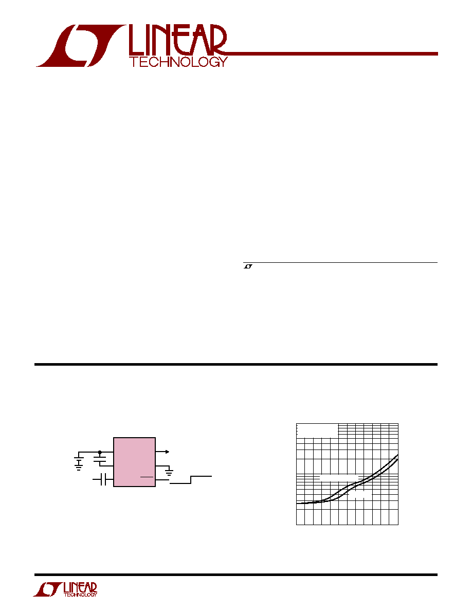
TYPICAL APPLICATIO
U
s
Wireless Transceivers
s
Wireless and Cable Infrastructure
s
RF Power Alarm
s
Envelope Detector
s
Temperature Compensated Internal Schottky
Diode RF Detector
s
Wide Input Power Range: 34dBm to 14dBm
s
Ultra Wide Input Frequency Range: 100kHz to
1000MHz
s
Buffered Output
s
Wide V
CC
Range of 2.7V to 6V
s
Low Operating Current: 550
µ
A
s
Low Shutdown Current: <2
µ
A
s
Low Profile (1mm) ThinSOT
TM
Package
100kHz to 1GHz
RF Power Detector
The LTC
®
5507 is an RF power detector for applications
operating from 100kHz to 1000MHz. The input frequency
range is determined by an external capacitor. A tempera-
ture-compensated Schottky diode peak detector and buffer
amplifier are combined in a small 6-pin ThinSOT package.
The RF input voltage is peak detected using an on-chip
Schottky diode and external capacitor. The detected volt-
age is buffered and supplied to the V
OUT
pin. A power
saving shutdown mode reduces supply current to less
than 2
µ
A.
, LTC and LT are registered trademarks of Linear Technology Corporation.
ThinSOT is a trademark of Linear Technology Corporation
5507 TA01
V
OUT
GND
SHDN
V
CC
PCAP
RF
IN
LTC5507
4
5
6
3
2
1
V
OUT
DETECTED
VOLTAGE
V
BAT
2.7V TO 6V
C2
C1
RF
INPUT
DISABLE ENABLE
Figure 1. 100kHz to 1000MHz RF Power Detector
Typical Detector Characteristics
at 100kHz, 100MHz and 1000MHz
RF INPUT POWER (dBm)
V
OUT
OUTPUT VOLTAGE (mV)
10000
5507 TA01b
100
1000
26
6
14
2
10
18
34
100kHz, 100MHz
1000MHz
T
A
= 25
°
C
V
CC
= 2.7V TO 6V
LTC5507
2
5507f
V
CC
, V
OUT
to GND .................................... 0.3V to 6.5V
RF
IN
Voltage to GND ......................... (V
CC
±
1.8V) to 7V
SHDN Voltage to GND ................ 0.3V to (V
CC
+ 0.3V)
PCAP Voltage to GND ........................ (V
CC
1.8V) to 7V
I
VOUT
...................................................................... 5mA
Operating Temperature Range (Note 2) .. 40
°
C to 85
°
C
Maximum Junction Temperature ......................... 125
°
C
Storage Temperature Range ................ 65
°
C to 150
°
C
Lead Temperature (Soldering, 10 sec)................. 300
°
C
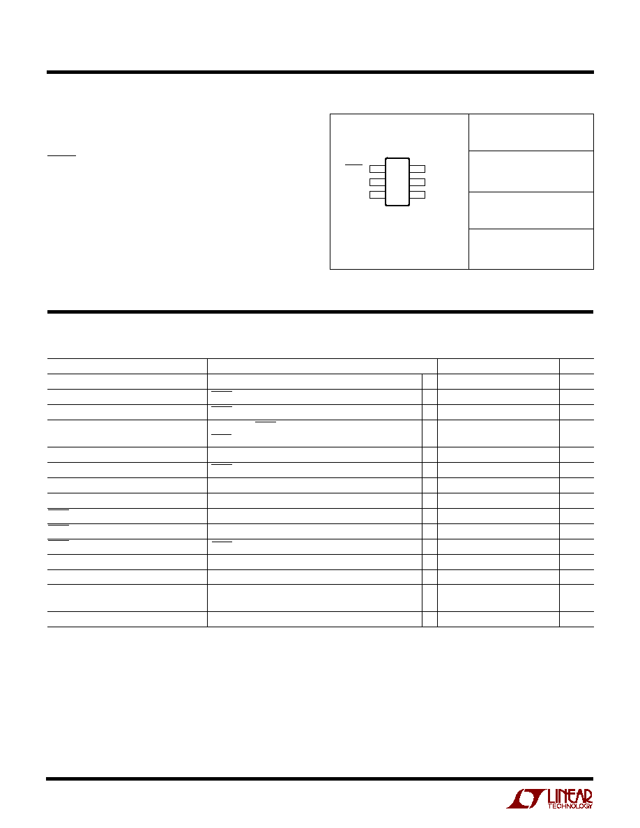
ORDER PART
NUMBER
S6 PART
MARKING
T
JMAX
= 125
°
C,
JA
= 250
°
C/W
LTZX
LTC5507ES6
ABSOLUTE AXI U
RATI GS
W
W
W
U
PACKAGE/ORDER I FOR ATIO
U
U
W
(Note 1)
ELECTRICAL CHARACTERISTICS
The
q
denotes the specifications which apply over the full operating
temperature range, otherwise specifications are at T
A
= 25
°
C. V
CC
= 3.6V, RF Input Signal is Off, unless otherwise noted.
PARAMETER
CONDITIONS
MIN
TYP
MAX
UNITS
V
CC
Operating Voltage
q
2.7
6
V
I
VCC
Shutdown Current
SHDN = 0V
q
2
µ
A
I
VCC
Operating Current
SHDN = V
CC
, I
VOUT
= 0mA
q
0.55
0.85
mA
V
OUT
V
OL
(No RF Input)
R
LOAD
= 2k, SHDN = V
CC
, Enabled
130
250
370
mV
SHDN = 0V, Disabled
1
mV
V
OUT
Output Current
V
OUT
= 1.75V, V
CC
= 2.7V to 6V,
V
OUT
= 10mV
q
1
2
mA
V
OUT
Enable Time
SHDN = V
CC
, C
LOAD
= 33pF, R
LOAD
= 2k
q
7
20
µ
s
V
OUT
Load Capacitance
(Note 4)
q
33
pF
V
OUT
Noise
V
CC
= 3V, Noise BW = 1.5MHz, 50
RF Input Termination
2
mV
P-P
SHDN Voltage, Chip Disabled
V
CC
= 2.7V to 6V
q
0.35
V
SHDN Voltage, Chip Enabled
V
CC
= 2.7V to 6V
q
1.4
V
SHDN Input Current
SHDN = 3.6V
q
24
40
µ
A
RF
IN
Input Frequency Range
0.1 1000
MHz
Max RF
IN
Input Power
(Note 3)
14
dBm
RF
IN
AC Input Resistance
F = 10MHz, RF Input = 10dBm
130
F = 1000MHz, RF Input = 10dBm
95
RF
IN
Input Shunt Capacitance
1.7
pF
Consult LTC Marketing for parts specified with wider operating temperature ranges.
Note 1: Absolute Maximum Ratings are those values beyond which the life
of a device may be impaired.
Note 2: Specifications over the 40
°
C to 85
°
C operating temperature
range are assured by design, characterization and correlation with
statistical process controls.
Note 3: RF performance is tested at: 80MHz, 4dBm
Note 4: Guaranteed by design.
6 RF
IN
5 PCAP
4 V
CC
SHDN 1
TOP VIEW
S6 PACKAGE
6-LEAD PLASTIC SOT-23
GND 2
V
OUT
3
LTC5507
3
5507f
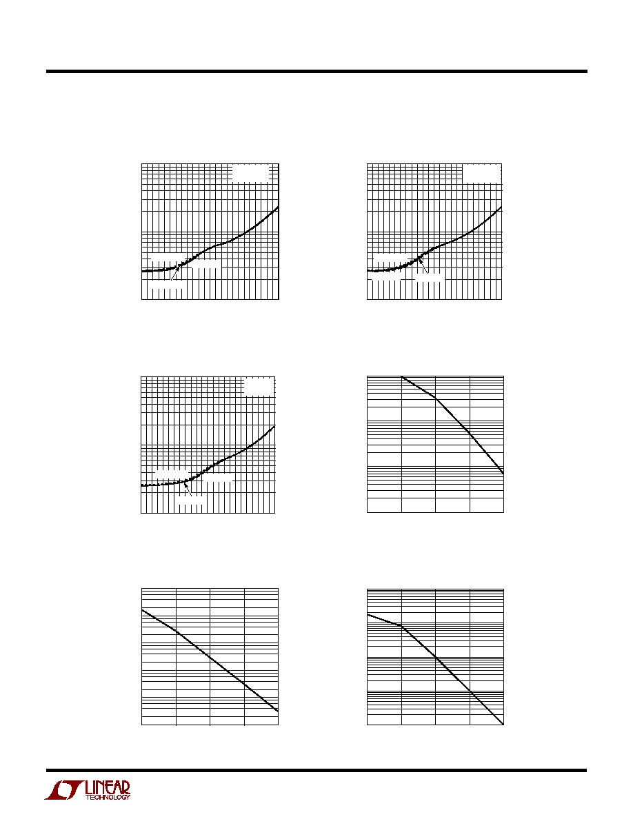
TYPICAL PERFOR A CE CHARACTERISTICS
U
W
LTC5507 Typical Detector
Characteristics, 100kHz,
V
CC
= 2.7V TO 6V
Positive V
OUT
Slew Rate vs C2
Capacitance
LTC5507 Typical Detector
Characteristics, 1000MHz
V
CC
= 2.7V TO 6V
LTC5507 Typical Detector
Characteristics, 100MHz
V
CC
= 2.7V TO 6V
RF INPUT POWER (dBm)
34 28
22 16
V
OUT
OUTPUT VOLTAGE (mV)
100
1000
10000
10
4
2
8
14
5507 G01
T
A
= 40
°
C
T
A
= 85
°
C
C1 = 0.47
µ
F
C2 = 0.47
µ
F
T
A
= 25
°
C
T
A
= 40
°
C
T
A
= 85
°
C
C1 = 1000pF
C2 = 1000pF
T
A
= 25
°
C
RF INPUT POWER (dBm)
34 28
22 16
V
OUT
OUTPUT VOLTAGE (mV)
100
1000
10000
10
4
2
8
14
5507 G02
T
A
= 40
°
C
T
A
= 85
°
C
C1 = 33pF
C2 = 33pF
T
A
= 25
°
C
RF INPUT POWER (dBm)
34 28
22 16
V
OUT
OUTPUT VOLTAGE (mV)
100
1000
10000
10
4
2
8
14
5507 G03
C2 CAPACITANCE (pF)
33
POSITIVE V
OUT
SLEW RATE (V/
µ
s)
10.0
1.0
0.10
0.01
330
3300
330000
33000
5507 G04
C2 CAPACITANCE (pF)
33
330
3300
330000
33000
5507 G05
NEGATIVE V
OUT
SLEW RATE (V/
µ
s)
10.000
1.000
0.100
0.010
0.001
0
C2 CAPACITANCE (pF)
33
330
3300
330000
33000
5507 G06
V
OUT
BW (kHz)
10000
1000
100
10
1
V
OUT
BW vs C2 Capacitance
Negative V
OUT
Slew Rate vs C2
Capacitance
LTC5507
4
5507f
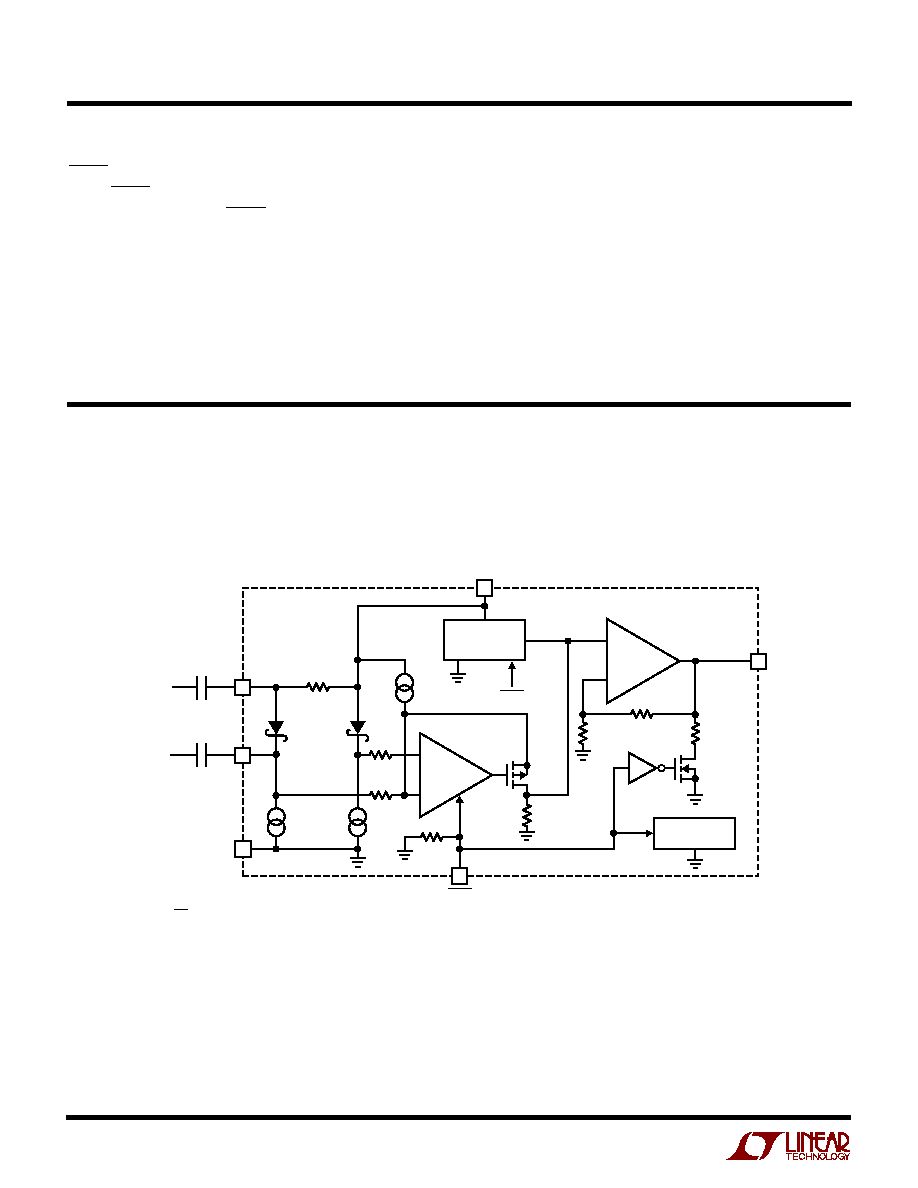
BLOCK DIAGRA
W
+
+
5507 BD
GAIN
COMPRESSION
SHDN
V
OUT
SHDN
GND
C1
C2
2
1
3
4
BUFFER
250
RF DET
30k
30k
60
µ
A
60
µ
A
150k
BIAS
100
RF
SOURCE
RF
IN
V
CC
6
5
V
CC
PCAP
C1 = C2
C2 (
µ
F)
, f = LOWEST RF INPUT FREQUENCY (MHz)
1
30f
U
U
U
PI FU CTIO S
SHDN (Pin 1): Shutdown Input. A logic low or no-connect
on the SHDN pin places the part in shutdown mode. A logic
high enables the part. SHDN has an internal 150k pull
down resistor to ensure that the part is in shutdown when
the enable driver is in a tri-state condition.
GND (Pin 2): System Ground.
V
OUT
(Pin 3): Buffered and Level Shifted Detector Output
Voltage.
V
CC
(Pin 4): Power Supply Voltage, 2.7V to 6V. V
CC
should
be bypassed with 0.1
µ
F and 100pF ceramic capacitors.
PCAP (Pin 5): Peak Detector Hold Capacitor. Capacitor
value is dependent on RF frequency. Capacitor must be
connected between PCAP and V
CC
.
RF
IN
(Pin 6): RF Input Voltage. Referenced to V
CC
. A
coupling capacitor must be used to connect to the RF
signal source. This pin has an internal 250
termination
and an internal Schottky diode detector.
Figure 2.

LTC5507
5
5507f
APPLICATIO S I FOR ATIO
W
U
U
U
Operation
The LTC5507 integrates several functions to provide RF
power detection over frequencies up to 1000MHz. These
functions include an internally compensated buffer ampli-
fier, an RF Schottky diode peak detector and level shift
amplifier to convert the RF signal to DC, a delay circuit to
avoid voltage transients at V
OUT
when coming out of shut-
down, and a gain compression circuit to extend the
detector dynamic range.
Buffer Amplifier
The buffer amplifier has a gain of two and is capable of
driving a 2mA load. The buffer amplifier typically has an
output voltage range of 0.25V to V
CC
0.1V.
RF Detector
The internal RF Schottky diode peak detector and level
shift amplifier converts the RF input signal to a low
frequency signal. The frequency range of the RF pin is
typically up to 1000MHz. The detector demonstrates ex-
cellent operation over a wide range of input power. The
Schottky detector is biased at about 70
µ
A. The hold
capacitor is external.
Gain Compression
The gain compression circuit changes the feedback ratio
as the RF peak-detected input voltage increases above
60mV. Below 60mV, the DC voltage gain from the peak
detector to the buffer output is 4. Above 140mV, the DC
voltage gain is reduced to 0.75. The compression expands
the low power detector range due to higher gain.
Modes of Operation
MODE
SHDN
OPERATION
Shutdown
Low
Disabled
Enable
High
Power Detect
Applications
The LTC5507 can be used as a self-standing signal strength
measuring receiver for a wide range of input signals from
34dBm to 14dBm for frequencies up to 1000MHz.
The LTC5507 can be used as a demodulator for AM and
ASK modulated signals with data rates up to 1.5MHz.
Depending on specific application needs, the RSSI output
can be split into two branches, providing AC-coupled data
(or audio) output and DC-coupled, RSSI output for signal
strength measurements and AGC.
C1, C2 Capacitor Selection (Refer to Figure 3)
C1 couples the RF input signal to the detector input RF
IN
which is referenced to V
CC
. C2 is the peak detector
capacitor connected between PCAP and V
CC
. The value of
C2 will affect the slew rate and bandwidth. Typically C1 can
equal C2. Ceramic capacitors are recommended for C1
and C2. The values for C1 and C2 are dependent on the
operating RF frequency. The capacitive reactance should
be less than 5
to minimize ripple on C2.
C2(
µ
F)
1/(30 · f) where f is the lowest RF input
frequency (MHz)
C1 = C2
In general, select C1 and C2 large enough to pass the
lowest expected RF signal frequency, as described by the
above formulas. But optimize C1 and C2, subject to this
constraint, to improve output slew rate and bandwidth,
and to enable good AC performance for the highest
expected RF signal frequency.