LTC3422
1
3422f
Wireless Handsets
Handheld Computers
GPS Receivers
MP3 Players
700mA Continuous/1A Pulsed Output Current
for Li-Ion to 5V Applications
Synchronous Rectification: Up to 96% Efficiency
True Output Disconnect
Inrush Current Limiting
Adjustable Automatic Burst Mode
Û
Operation
Low Noise, Fixed Frequency Operation from
100kHz to 3MHz
0.5V to 4.5V Input Range
2.25V to 5.25V Adjustable Output Voltage
Guaranteed 1V Start-Up
Programmable Soft-Start
Synchronizable Oscillator
Low Quiescent Current: 25
çA
< 1
çA Shutdown Current
Anti-Ringing Control
Small (3mm
æ 3mm æ 0.75mm) Thermally Enhanced
10-Pin DFN Package
1.5A, 3MHz Synchronous
Step-Up DC/DC Converter
with Output Disconnect
2.4V to 3.3V Efficiency and Power Loss
DESCRIPTIO
U
FEATURES
APPLICATIO S
U
TYPICAL APPLICATIO
U
The LTC
Û
3422 is a high efficiency, current mode, fixed
frequency, step-up DC/DC converter with true output
disconnect and inrush current limiting. The part is guaran-
teed to start up from an input voltage of 1V. The device
includes a 0.20
N-channel MOSFET switch and a 0.24
P-channel MOSFET synchronous rectifier. The output
voltage, switching frequency, soft-start time, Burst Mode
threshold and loop compensation are all simply pro-
grammed using tiny external passive components.
Quiescent current is only 25
çA during Burst Mode opera-
tion, maximizing battery life in portable applications. The
oscillator frequency can be programmed up to 3MHz and
can be synchronized to an external clock applied to the
SYNC pin.
Other features include 1
çA shutdown, short-circuit protec-
tion, anti-ringing control, thermal shutdown and current
limit. The LTC3422 is available in a (3mm
æ 3mm æ 0.75mm)
10-pin DFN package.
, LTC and LT are registered trademarks of Linear Technology Corporation.
Burst Mode is a registered trademark of Linear Technology Corporation.
All other trademarks are the property of their respective owners.
0.1
çF
1nF
OFF ON
15k
22
çF
4.7
çF
V
IN
1.8V TO 3.2V
2 CELLS
+
1nF
28k
931k
V
OUT
3.3V
600mA
549k
301k
3422 TA01a
SS
V
C
BURST
SHDN
FB
SYNC
V
OUT
R
T
GND
V
IN
LTC3422
4.7
çH
SW
20pF
LOAD CURRENT (mA)
30
EFFICIENCY (%)
POWER LOSS (mW)
90
100
20
10
80
50
70
60
40
0.1
10
100
1000
3422 TA01b
0
1000
10000
100
10
1
0
1
BURST
EFFICIENCY
PWM
EFFICIENCY
BURST
POWER
LOSSES
f
OSC
= 1MHz
PWM
POWER
LOSSES
LTC3422
2
3422f
PARAMETER
CONDITIONS
MIN
TYP
MAX
UNITS
Minimum V
IN
Start-Up Voltage
I
LOAD
< 1mA
0.88
1
V
Minimum V
IN
Operating Voltage
(Note 3)
0.5
V
Output Voltage Adjust Range
2.25
5.25
V
2.40
5.25
V
Feedback Voltage
1.192
1.216
1.240
V
Feedback Input Current
V
FB
= 1.216V
1
50
nA
Quiescent Current--Burst Mode Operation
V
C
= 0V (Note 4)
25
42
çA
Quiescent Current--Shutdown
SHDN = 0V, V
OUT
= 0V
0.1
1
çA
Quiescent Current--Active
V
C
= 0V (Note 4)
0.75
1.1
mA
NMOS Switch Leakage
0.1
5
çA
PMOS Switch Leakage
V
OUT
= 2V
0.1
10
çA
NMOS Switch On Resistance
V
OUT
= 3.3V
0.20
PMOS Switch On Resistance
V
OUT
= 3.3V
0.24
NMOS Current Limit--Steady State
1.5
A
NMOS Current Limit--Pulsed
Duty Cycle Not to Exceed 5%
2
2.5
A
NMOS Current Limit--Short Circuit
V
OUT
= 500mV
0.75
1.5
A
NMOS Burst Current Limit
600
mA
Maximum Duty Cycle
84
91
%
Minimum Duty Cycle
0
%
Frequency Accuracy
0.85
1
1.15
MHz
SYNC Input High
2.2
V
SYNC Input Low
0.8
V
SYNC Input Current
0.01
1
çA
V
IN
, V
OUT
, SYNC Voltages ........................... Ù 0.3V to 6V
SS, BURST, SHDN Voltages ...................... Ù 0.3V to 6V
SW Voltage
DC .......................................................... Ù 0.3V to 6V
Pulsed < 100ns ...................................... Ù 0.3V to 7V
Operating Temperature Range
(Notes 2, 5) ............................................. Ù40
¯C to 85¯C
Storage Temperature Range ................. Ù 65
¯C to 125¯C
ORDER PART NUMBER
Consult LTC Marketing for parts specified with wider operating temperature ranges.
LTC3422EDD
ABSOLUTE AXI U
RATI GS
W
W
W
U
PACKAGE/ORDER I FOR ATIO
U
U
W
(Note 1)
T
JMAX
= 125
¯C,
JA
= 43
¯C/W
EXPOSED PAD (PIN 11) IS GND, MUST BE SOLDERED TO PCB
ELECTRICAL CHARACTERISTICS
The
denotes the specifications which apply over the full operating
temperature range, otherwise specifications are at T
A
= 25
¯C. V
IN
= 1.2V, V
OUT
= 3.3V, R
T
= 28k, unless otherwise noted. (Note 2)
TOP VIEW
11
DD PACKAGE
10-LEAD (3mm
æ 3mm) PLASTIC DFN
10
9
6
7
8
4
5
3
2
1
V
OUT
SYNC
R
T
V
C
FB
SW
V
IN
BURST
SS
SHDN
DD PART MARKING
LBRN
Order Options Tape and Reel: Add #TR
Lead Free: Add #PBF Lead Free Tape and Reel: Add #TRPBF
Lead Free Part Marking:
http://www.linear.com/leadfree/
LTC3422
3
3422f
Note 1: Absolute Maximum Ratings are those values beyond which the life
of a device may be impaired.
Note 2: The LTC3422E is guaranteed to meet performance specifications
from 0
¯C to 70¯C. Specifications over the Ù40¯C to 85¯C operating
temperature range are assured by design, characterization and correlation
with statistical process controls.
Note 3: Once V
OUT
is greater than 2.4V, the LTC3422 is not dependent on
the V
IN
supply.
Note 4: Current is measured into the V
OUT
pin since the supply current is
bootstrapped to the output. The current will reflect to the input supply by
(V
OUT
/V
IN
) ñ Efficiency. The outputs are not switching.
Note 5: This IC includes overtemperature protection that is intended to
protect the device during momentary overload conditions. Junction
temperature will exceed 125
¯C when overtemperature protection is active.
Continuous operation above the specified maximum operating junction
temperature may impair device reliability.
PARAMETER
CONDITIONS
MIN
TYP
MAX
UNITS
SHDN Input High
V
OUT
= 0V (Turn-On Threshold, Initial Start-Up)
1
V
V
OUT
> 2.4V (Stay-On Threshold)
0.65
V
SHDN Input Low
Turn-Off Threshold
0.25
V
SHDN Input Current
V
SHDN
= 3.3V
0.01
1
çA
Error Amp Transconductance
50
çS
Soft-Start Current Source
V
SS
= 1V
Ù5
Ù2.4
Ù1.2
çA
BURST Threshold Voltage
Falling Edge, Sensed at the BURST Pin
0.79
0.88
0.97
V
ELECTRICAL CHARACTERISTICS
The
denotes the specifications which apply over the full operating
temperature range, otherwise specifications are at T
A
= 25
¯C. V
IN
= 1.2V, V
OUT
= 3.3V, R
T
= 28k, unless otherwise noted. (Note 2)
LTC3422
4
3422f
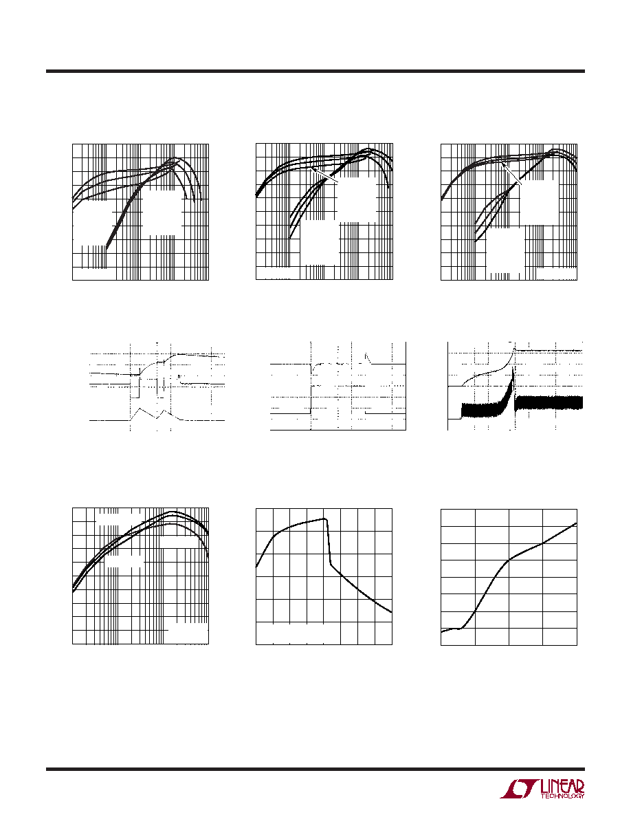
TYPICAL PERFOR A CE CHARACTERISTICS
U
W
Single Cell to 3.3V Efficiency
2-Cell to 3.3V Efficiency
Li-Ion to 5V Efficiency
Burst Mode Operation
Load Transient Response
Inrush Current Control
Efficiency vs Frequency
Efficiency vs V
IN
Start-Up Voltage vs Output Current
OUTPUT CURRENT (mA)
1
40
EFFICIENCY (%)
50
60
70
80
10
100
1000
3422 G07
30
20
10
0
90
100
V
IN
= 2.4V
V
OUT
= 3.3V
f
OSC
= 300kHz
f
OSC
= 3MHz
f
OSC
= 1MHz
INPUT VOLTAGE (V)
1
EFFICIENCY (%)
40
50
100
70
2
3
3.5
3422 G08
80
90
60
1.5
2.5
4
4.5
5
V
OUT
= 3.3V
PWM AT 200mA LOAD
OUTPUT CURRENT (mA)
0
START VOLTAGE (V)
1.00
1.05
1.10
200
3422 G09
0.95
0.90
50
100
150
0.85
1.20
1.25
1.15
V
OUT
50mV/DIV
AC COUPLED
SW
2V/DIV
INDUCTOR
CURRENT
0.5A/DIV
V
IN
= 2.4V
I
LOAD
= 20mA
2
çs/DIV
3422 G04
V
OUT
100mV/DIV
AC COUPLED
I
OUT
100mA/DIV
V
IN
= 2.4V
V
OUT
= 3.3V
C
OUT
= 22
çF
200
çs/DIV
3422 G05
300mA
50mA
V
OUT
1V/DIV
INDUCTOR
CURRENT
100mA/DIV
V
IN
= 0V TO 2.4V
V
OUT
= 3.3V
C
OUT
= 22
çF
100mA LOAD CURRENT
500
çs/DIV
3422 G06
(T
A
= 25
¯C, unless otherwise specified)
LOAD CURRENT (mA)
30
EFFICIENCY (%)
90
100
20
10
80
50
70
60
40
0.1
10
100
1000
3422 G01
0
1
BURST
EFFICIENCY
V
IN
= 1.6V
V
IN
= 1.25V
V
IN
= 0.9V
PWM
EFFICIENCY
V
IN
= 1.6V
V
IN
= 1.25V
V
IN
= 0.9V
f
OSC
= 1MHz
LOAD CURRENT (mA)
30
EFFICIENCY (%)
90
100
20
10
80
50
70
60
40
0.1
10
100
1000
3422 G02
0
1
PWM
EFFICIENCY
V
IN
= 3V
V
IN
= 2.4V
V
IN
= 1.8V
f
OSC
= 1MHz
BURST
EFFICIENCY
V
IN
= 3V
V
IN
= 2.4V
V
IN
= 1.8V
LOAD CURRENT (mA)
30
EFFICIENCY (%)
90
100
20
10
80
50
70
60
40
0.1
10
100
1000
3422 G03
0
1
BURST
EFFICIENCY
V
IN
= 4.2V
V
IN
= 3.6V
V
IN
= 3.1V
PWM
EFFICIENCY
V
IN
= 4.2V
V
IN
= 3.6V
V
IN
= 3.1V
f
OSC
= 1MHz
LTC3422
5
3422f
Burst Mode Output Current
Threshold vs R
BURST
(3.3V Output)
FB Voltage vs Temperature
Frequency Accuracy vs
Temperature (Normalized
About 1MHz)
Burst Mode Quiescent Current
vs Temperature
Current Limit Accuracy
vs Temperature
R
DS(ON)
vs Temperature
TYPICAL PERFOR A CE CHARACTERISTICS
U
W
(T
A
= 25
¯C, unless otherwise specified)
R
BURST
(k
)
50
OUTPUT CURRENT (mA)
120
140
100
80
40
20
350
550 650 750 850
3422 G10
60
0
150 250
450
V
IN
= 1.25V TO 2.9V
V
OUT
= 3.3V
f
OSC
= 1MHz
EXITS BURST (AVE)
ENTERS BURST (MIN)
R
BURST
(k
)
50
OUTPUT CURRENT (mA)
120
140
100
80
40
20
275
425 500 575 650
3422 G11
60
0
125 200
350
V
IN
= 1.8V TO 4.2V
V
OUT
= 5V
f
OSC
= 1MHz
EXITS BURST (AVE)
ENTERS BURST (MIN)
TEMPERATURE (
¯C)
Ù45
1.213
VOLTAGE (V)
1.214
1.215
1.216
1.217
Ù30 Ù15
0
15
3422 G12
30
45
60
75
90
TEMPERATURE (
¯C)
Ù45
0.98
FREQUENCY (MHz)
0.99
1.00
1.01
1.02
Ù30 Ù15
0
15
3422 G13
30
45
60
75
90
TEMPERATURE (
¯C)
Ù45
22
QUIESCENT CURRENT (
ç
A)
24
26
28
30
Ù30 Ù15
0
15
3422 G14
30
45
60
75
90
TEMPERATURE (
¯C)
Ù45
2.35
CURRENT (A)
2.40
2.45
2.50
2.55
Ù30 Ù15
0
15
3422 G15
30
45
60
75
90
No-Load Input Current vs V
IN
Maximum Output Current vs V
IN
Burst Mode Output Current
Threshold vs R
BURST
(5V Output)
TEMPERATURE (
¯C)
Ù45
160
RESISTANCE (m
)
280
260
240
220
200
180
Ù30 Ù15
0
15
3422 G16
30
45
60
75
90
PMOS R
DS(ON)
NMOS R
DS(ON)
INPUT VOLTAGE (V)
0.8
50
INPUT CURRENT (
ç
A)
70
90
100
170
140
1.6
2.4 2.8
4.4
160
150
120
60
80
130
110
1.2
2
3.2 3.6
4
4.8
3422 G17
CHIP ENTERS
Burst Mode OPERATION
V
OUT
= 5V
V
OUT
= 3.3V
INPUT VOLTAGE (V)
1.80
OUTPUT CURRENT (mA)
1200
1400
1600
5.40
3422 G18
1000
800
400
2.40
3.00
3.60
4.20
4.80
600
2000
1800
f
OSC
= 1MHz
V
OUT
= 3.3V
V
OUT
= 5V
3.3V DIODE
RECTIFICATION
5V DIODE
RECTIFICATION

LTC3422
6
3422f
PI FU CTIO S
U
U
U
SW (Pin 1): Switch Pin for the Inductor Connection.
Minimize trace length between SW and inductor. For
discontinuous inductor current, a controlled impedance is
internally connected from SW to V
IN
to eliminate high
frequency ringing, reducing EMI radiation.
V
IN
(Pin 2): Input Supply Voltage. Connect V
IN
to the input
supply and decouple with a 4.7
çF or larger ceramic
capacitor as close to V
IN
as possible.
BURST (Pin 3): Burst Mode
Threshold Adjust. Automatic
Burst Mode Operation: A resistor/capacitor combination
from BURST to ground programs the average load current
at which automatic Burst Mode operation is exited, ac-
cording to the formula:
R
I
B
EXITBURST
=
12
where R
B
is in k
and I
EXITBURST
is in amps
C
C
V
B
OUT
OUT
ñ
,
64 000
where C
B(MIN)
and C
OUT
are in
çF.
Please refer to the Burst Mode Output Current Threshold
vs R
BURST
Typical Performance Chacteristic curves.
Note that during Burst Mode operation the peak inductor
current will be approximately 600mA and return to zero on each
cycle. In Burst Mode operation the frequency is variable,
providing a significant efficiency improvement at light loads.
The LTC3422 only allows Burst Mode operation to be entered
once V
OUT
exceeds approximately 2.2V.
Manually Implementing Burst Mode Operation: Ground
BURST to force Burst Mode operation or connect it to V
OUT
to
force fixed frequency PWM mode. Note that BURST must not
be pulled higher than V
OUT
.
SS (Pin 4): Soft-Start. Connect a capacitor from SS to ground to
set the soft-start time according to the formula:
t(ms) = C
SS
(
çF) ñ 320
The nominal soft-start charging current is 2.4
çA. The active
range of SS is from 0.8V to 1.6V.
SHDN (Pin 5): Shutdown Input. Less than 250mV on SHDN
shuts down the LTC3422. Placing 1V or more on SHDN enables
the LTC3422. Once V
OUT
exceeds 2.2V, hysteresis is applied
to this pin (500nA exits the pin) allowing it to operate at a logic
high while the battery can drop to 500mV.
FB (Pin 6): Feedback Input to Error Amplifier. Connect the V
OUT
to ground resistor divider tap here. The output voltage can be
adjusted from 2.25V to 5.25V according to the formula:
V
R
R
R
OUT
=
+
1 216
1
2
2
.
ñ
V
C
(Pin 7): Error Amp Output. A frequency compensation
network is connected from V
C
to ground to compensate the
loop. See the section "Compensating the Feedback Loop" for
guidelines.
R
T
(Pin 8): Frequency Adjust Input. Connect a resistor to ground
to program the oscillator frequency according to the formula:
f
R
OSC
T
=
28
where f
OSC
is in MHz and R
T
is in k
.
SYNC (Pin 9): Oscillator Synchronization Input. A clock pulse
width of 100ns to 2
çs is required to synchronize the internal
oscillator. If not used, SYNC should be grounded.
V
OUT
(Pin 10): Output of the synchronous rectifier and
bootstrapped power source for the LTC3422. A ceramic capaci-
tor of at least 10
çF is required and should be located as close to
V
OUT
and the power ground plane as possible.
Exposed Pad (Pin 11): Signal and Power Ground for the
LTC3422. This pin MUST be soldered to the PCB ground plane
for electrical contact and rated thermal performance.
LTC3422
7
3422f
BLOCK DIAGRA
W
Ù
+
Ù
Ù
+
+
BULK
CONTROL
SIGNALS
CURRENT
SENSE
ANTIRING
OPTIONAL
L1
4.7
çH
CURRENT
SENSE
Ù
+
I
ZERO
COMP
BURST
COMP
AWAKEN
COMP
g
m
ERROR
AMPLIFIER
PWM
COMP
PWM
LOGIC
AND
DRIVERS
BURST SLEEP
BURST
MODE
CONTROL
V
IN
SW
1
R
T
8
SYNC
R
T
28k
9
BURST
3422 BD
3
SS
4
FB
6
V
C
7
V
OUT
V
IN
10
EXPOSED
PAD
11
2
SHDN
C
IN
10
çF
5
SHUTDOWN
AND
V
BIAS
SHDN
0.88V
Ù
+
Ù
+
1.216V
1.5A
+
+
START-UP
CURRENT
RAMP
Ù
+
Ù2%
REFERENCE
THERMAL
SHUTDOWN
START-UP
SOFT-START
AND
THERMAL
REG
1.216V
0.88V
SLOPE
COMPENSATION
OSCILLATOR
I
MAX
COMP
R
B
301k
C
B
1nF
C
SS
0.1
çF
R1
C
OUT
22
çF
R2
R
Z
15k
C
C1
1nF
C
C2
20pF
V
OUT
2.25V TO 5.25
V
IN
1V TO 4.5V
OPERATIO
U
LOW VOLTAGE START-UP
The LTC3422 includes an independent start-up oscillator
designed to start up at input voltages of 0.88V typical.
During start-up, the peak current limit is gradually
increased in conjunction with the soft-start ramp. Switch-
ing frequency is also internally controlled during start-up.
The device can start up under some load (see graph of
Start-Up Voltage versus Output Current). Soft-start and

LTC3422
8
3422f
OPERATIO
U
inrush current limiting are provided during start-up as
well as normal switching mode. The same soft-start
capacitor is used for each operating mode.
When either V
IN
or V
OUT
exceeds 2.25V, the LTC3422
enters normal operating mode. Once the output voltage
exceeds the input by 0.3V typical, the LTC3422 powers
itself from V
OUT
instead of V
IN
. At this point the internal
circuitry has no dependency on the V
IN
input voltage,
eliminating the requirement for a large input capacitor.
The input voltage can drop as low as 0.5V without affecting
circuit operation. The limiting factor for the application
becomes the availability of the power source to supply
sufficient energy to the output at the low voltages and the
maximum duty cycle, which is clamped at 91% typical.
LOW NOISE FIXED FREQUENCY OPERATION
Shutdown
The part is shutdown by pulling SHDN below 0.25V, and
activated by pulling the pin initially above 1V. Once V
OUT
exceeds 2.2V typical, hysteresis is applied to this pin
allowing it to maintain a logic high state down to 0.65V.
Note that SHDN can be driven above V
IN
or V
OUT
as long
as it is limited to less than the absolute maximum rating.
Soft-Start
The soft-start time is programmed with an external capaci-
tor from SS to ground. An internal current source charges
it with a nominal 2.4
çA. The ramping voltage on SS
dictates the gradually increasing peak current limit until
the voltage on the capacitor exceeds 1.6V, after which the
internally set peak current limit is maintained. In the event
of a commanded shutdown or a thermal shutdown, the
capacitor on SS is discharged to ground automatically.
Note that Burst Mode operation is inhibited during the
soft-start time.
t (ms) = C
SS
(
çF) ñ 320
Oscillator
The frequency of operation is set through a resistor from
R
T
to ground. A precision timing capacitor resides inside
the LTC3422. The oscillator can be synchronized with an
external clock applied to SYNC. When synchronizing the
oscillator, the free running frequency must be set at least
20% lower than the desired synchronized frequency.
f
R
OSC
T
=
28
where f
OSC
is in MHz and R
T
is in k
.
Current Sensing
Lossless current sensing converts the peak current signal
to a voltage to sum in with the internal slope compensa-
tion. This summed signal is compared to the error ampli-
fier output to provide a peak current control command for
the PWM. The LTC3422 incorporates slope compensation
which is adaptive to the input and output voltages. There-
fore, the converter provides the proper amount of slope
compensation to ensure stability, but not an excess which
would cause a loss of phase margin in the converter.
Error Amplifier
The error amplifier is a transconductance amplifier, with
its positive input internally connected to the 1.216V refer-
ence and its negative input connected to FB. A simple
compensation network is placed from V
C
to ground.
Internal clamps limit the minimum and maximum error
amplifier output voltage for improved large-signal tran-
sient response.
Current Limit
The current limit circuitry shuts off the internal N-channel
MOSFET switch when the current limit threshold is reached.
In Burst Mode operation, the current limit is reduced to
approximately 600mA.
Zero Current Amplifier
The zero current amplifier monitors the inductor current to
the output and shuts off the synchronous rectifier once the
current falls below 50mA typical, preventing negative
inductor current.
Anti-Ringing Control
The anti-ringing control connects a resistor across the
inductor to dampen the ringing on SW during discontinu-
ous conduction mode. The LC
SW
ringing (L = inductor,

LTC3422
9
3422f
OPERATIO
U
C
SW
= SW Capacitance) is low energy, but can cause EMI
radiation.
Burst Mode OPERATION
Burst Mode operation can be automatic or user controlled.
In automatic operation, the LTC3422 will automatically
enter Burst Mode operation at light load and return to fixed
frequency PWM mode for heavier loads. The user can
program the average load current at which the mode
transition occurs using a single resistor connected from
BURST to GND.
The oscillator is shut down during Burst Mode operation,
since the on time is determined by the time it takes the
inductor current to reach a fixed 600mA peak current and
the off time is determined by the time it takes for the
inductor current to return to zero.
In Burst Mode operation, the LTC3422 delivers energy to
the output until it is regulated and then enters a sleep state,
where the switches are kept off while the LTC3422 con-
sumes only 25
çA of quiescent current. In this mode the
output ripple has a variable frequency component with
load current and will be typically 2% peak-peak. This
maximizes efficiency at very light loads by minimizing
switching and quiescent losses. Burst Mode operation
ripple can be reduced slightly by increasing the output
capacitance (47
çF or greater). This additional capacitance
does not need to be a low ESR type if low ESR ceramics are
also used. Another method of reducing Burst Mode opera-
tion ripple is to place a small feed-forward capacitor (10pF
to 100pF) across the upper resistor in the V
OUT
feedback
divider network.
In Burst Mode operation, the compensation network is not
used and V
C
is disconnected from the error amplifier.
During long periods of Burst Mode operation, leakage
currents in the external components or on the PC board
could cause the compensation capacitor to charge (or
discharge), which could result in a large output transient
when returning to fixed frequency mode of operation, even
at the same load current. To prevent this, the LTC3422
incorporates an active clamp circuit that holds the voltage
on V
C
at an optimal voltage during Burst Mode operation.
This minimizes any output transient when returning to
fixed frequency mode operation.
Automatic Burst Mode Operation Control
For automatic operation, an RC network should be con-
nected from BURST to ground. The value of the resistor
will control the average load current (I
BURST
) at which
Burst Mode operation will be entered and exited (there is
hysteresis to prevent oscillation between modes). The
equation given for the capacitor on BURST is the minimum
value to prevent ripple on BURST from causing the part to
oscillate in and out of Burst Mode operation at the current
where the mode transition occurs. The equation given for
the resistor on BURST is the typical average load current
at which automatic Burst Mode operation is exited.
R
I
B
EXITBURST
=
12
where R
B
is in k
and I
EXITBURST
is in amps.
C
C
V
B
OUT
OUT
ñ
,
64 000
where C
B(MIN)
and C
OUT
are in
çF.
Please refer to the Burst Mode Output Current Threshold
vs R
BURST
Typical Performance Chacteristic curves.
In the event that a load transient causes FB to drop by more
than 4% from the regulation value while in Burst Mode
operation, the LTC3422 will immediately switch to fixed
frequency operation and an internal pull-up will be mo-
mentarily applied to BURST, rapidly charging the BURST
capacitor. This prevents the LTC3422 from immediately
re-entering Burst Mode operation once the output achieves
regulation.
Manual Burst Mode Operation
For optimum transient response with large dynamic loads,
the operating mode should be controlled manually by the
host. By commanding fixed frequency PWM operation
prior to a sudden increase in load, output voltage droop
can be minimized. For manual control of Burst Mode
operation, the RC network connected to BURST can be
eliminated. To force fixed frequency PWM mode, BURST
should be connected to V
OUT
. To force Burst Mode opera-
tion, BURST should be grounded. When commanding
Burst Mode operation manually, the circuit connected to

LTC3422
10
3422f
OPERATIO
U
BURST must be able to sink up to 2mA. Burst Mode
operation is inhibited during soft-start.
If V
IN
is greater than V
OUT
Ù 300mV, the part will exit Burst
Mode operation and the synchronous rectifier will be
disabled.
Note that if the load current applied during
forced Burst
Mode operation (BURST is grounded) exceeds the current
that can be supplied, the output voltage will start to droop
and the LTC3422 will automatically come out of Burst
Mode operation and enter fixed frequency mode, raising
V
OUT
. Once regulation is achieved, the LTC3422 will then
enter Burst Mode operation once again (since the user is
still
commanding this by grounding BURST ) and the cycle
will repeat, resulting in about 4% output ripple. The
maximum average current that can be supplied in Burst
Mode operation is given by:
I
V
V
n mA
OUT MAX
IN
OUT
(
)
ñ
=
275
i
Output Disconnect and Inrush Limiting
The LTC3422 is designed to allow true output disconnect
by eliminating body diode conduction of the internal
P-channel MOSFET rectifier. This allows V
OUT
to go to zero
volts during shutdown without drawing any current from
2mA
880mV TO
1.16V
SSDONE
0 = PWM MODE
1 = Burst Mode
OPERATION
BURST
COMP
ERROR AMP/
SLEEP COMP
UVLO
COMP
V
CC
BURST
SLEEP
C
C1
C
B
R
Z
R
B
V
C
I
OUT
10,500
V
REF
Ù 4%
V
REF
Ý1%
Ù
+
Ù
+
Ù
+
COMP CLAMP
500mV TO 1V
7
BURST
3422 AI01
3
FB
6
Simplified Diagram of Automatic Burst Mode Control Circuit
LTC3422
11
3422f
OPERATIO
U
APPLICATIO S I FOR ATIO
W
U
U
U
the input source. It also allows for inrush current limiting
at turn-on, minimizing surge currents seen by the input
supply. Note that to obtain the advantages of output
disconnect, there must not be any external Schottky
diodes connected between the SW pin and V
OUT
.
Note: Board layout is extremely critical to minimize voltage
overshoot on SW due to stray inductance. Keep the output
filter capacitors as close as possible to V
OUT
and use very
low ESR/ESL ceramic capacitors tied to a good ground
plane.
where:
f = Operating Frequency in MHz
Ripple = Allowable Inductor Current Ripple (Amps
Peak-Peak)
V
IN(MIN)
= Minimum Input Voltage
V
OUT(MAX)
= Maximum Output Voltage
The inductor current ripple is typically set 20% to 40% of
the maximum inductor current.
For high efficiency, choose an inductor with high fre-
quency core material, such as ferrite, to reduce core
losses. The inductor should have low ESR (equivalent
series resistance) to reduce the I
2
R losses and must be
able to handle the peak inductor current without saturat-
ing. Molded chokes or chip inductors usually do not have
enough core to support peak inductor currents in the 2A
to 3A region. To minimize radiated noise, use a toroidal or
shielded inductor. See Table 1 for suggested inductor
suppliers and Table 2 for a list of capacitor suppliers.
Table 1. Inductor Vendor Information
SUPPLIER PHONE
FAX
WEB SITE
Coilcraft
(847) 639-6400
(847) 639-1469 www.coilcraft.com
CoEv
(800) 277-7040
(650) 361-2508 www.circuitprotection.
Magnetics
com/magnetics.asp
Murata
USA:
USA:
www.murata.com
(814) 237-1431
(814) 238-0490
(800) 831-9172
Sumida
USA:
USA:
www.sumida.com
(847) 956-0666
(847) 956-0702
Japan:
Japan:
81-3-3607-5111 81-3-3607-5144
TDK
(847) 803-6100
(847) 803-6296 www.component.tdk.com
TOKO
(847) 297-0070
(847) 669-7864 www.toko.com
Wurth
(201) 785-8800
(201) 785-8810 www.we-online.com
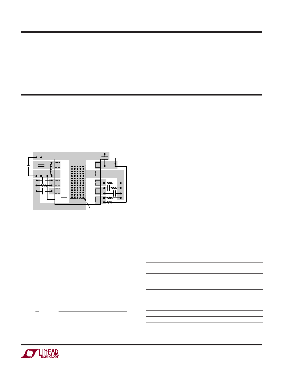
SW
1
V
IN
V
IN
2
BURST
3
SS
4
SHDN
MULTIPLE VIAS
TO GROUND PLANE
LTC3422
V
OUT
V
OUT
SYNC
R
T
V
C
FB
3422 F01
5
10
9
8
7
6
+
Figure 1. Recommended Component Placement. Traces
Carrying High Current are Direct (GND, SW, V
IN
, V
OUT
). Trace
Area at FB and V
C
are Kept Low. Lead Length to Battery Should
be Kept Short. V
IN
and V
OUT
Ceramic Capacitors Should be as
Close to the LTC3422 Pins as Possible
COMPONENT SELECTION
Inductor Selection
The high frequency operation of the LTC3422 allows the
use of small surface mount inductors. The minimum
inductance value is proportional to the operating fre-
quency and is limited by the following constraints:
L
V
V
OUT MAX
IN MIN
>
(
)
3
and L >
V
ñ Ripple ñ V
IN(MIN)
OUT(MAX)
ñ
Ù
(
)
(
)
It should also be noted that the LTC3422 provides inrush
current limiting without reducing the maximum load cur-
rent capability during start-up. The internally set peak
current command of the LTC3422 is allowed to gradually
increase during the soft-start period until it reaches the
nominal maximum level.

LTC3422
12
3422f
APPLICATIO S I FOR ATIO
W
U
U
U
Output Capacitor Selection
The output voltage ripple has two components to it. The
bulk value of the capacitor is set to reduce the ripple due
to charge into the capacitor each cycle. The maximum
ripple due to charge is given by:
V
I
V
C
V
R BULK
P
IN
OUT
OUT
(
)
ñ
ñ
ñ
=
where I
P
= peak inductor current
The ESR (equivalent series resistance) is usually the most
dominant factor for ripple in most power converters. The
ripple due to capacitor ESR is simply given by:
V
RCESR
= I
P
ñ C
ESR
where C
ESR
= capacitor equivalent series resistance.
Low ESR capacitors should be used to minimize output
voltage ripple. For most applications, Murata or Taiyo
Yuden X5R ceramic capacitors are recommended.
Input Capacitor Selection
The input filter capacitor reduces peak currents drawn
from the input source and reduces input switching noise.
Since the LTC3422 can operate at voltages below 0.5V
once the output is regulated, the demand on the input
capacitor is much less. In most applications 1
çF per Amp
of peak input current is recommended. Taiyo Yuden offers
very low ESR ceramic capacitors, for example the 1
çF in
a 0603 case (JMK107BJ105MA).
Table 2. Capacitor Vendor Information
SUPPLIER
PHONE
FAX
WEB SITE
AVX
(803) 448-9411 (803) 448-1943 www.avxcorp.com
Sanyo
(619) 661-6322 (619) 661-1055 www.sanyovideo.com
TDK
(847) 803-6100 (847) 803-6296 www.component.tdk.com
Murata
USA:
USA:
www.murata.com
(814) 237-1431 (814) 238-0490
(800) 831-9172
Taiyo Yuden (408) 573-4150 (408) 573-4159 www.t-yuden.com
Operating Frequency Selection
There are several considerations in selecting the operating
frequency of the converter, such as, what are the sensitive
frequency bands that cannot tolerate any spectral noise.
Another consideration is the physical size of the converter.
As the operating frequency goes up, the inductor and filter
capacitors go down in value and size. The trade off is in
efficiency since the switching losses due to gate charge
are proportionally increasing with frequency. For example,
as shown in Figure 2, for a 2.4V to 3.3V converter, the
efficiency at 160mA is 9% less at 3MHz versus 300kHz.
OUTPUT CURRENT (mA)
1
40
EFFICIENCY (%)
50
60
70
80
10
100
1000
3422 F02
30
20
10
0
90
100
V
IN
= 2.4V
V
OUT
= 3.3V
f
OSC
= 300kHz
f
OSC
= 3MHz
Figure 2. 2.4V to 3.3V Efficiency vs Frequency of Operation
The final consideration is whether the application can
allow "pulse skipping." In this mode, the minimum on time
of the converter cannot support the duty cycle, so the
converter ripple will go up and there will be a low frequency
component of the output ripple. In many applications
where physical size is the main criterion, running the
converter in this mode is acceptable. In applications where
it is preferred not to enter this mode, the maximum
operating frequency is given by:
MAX NOSKIP
OUT
IN
OUT
ON MIN
V
V
V
t
Hz
_
(
)
Ù
ñ
=
where t
ON(MIN)
= minimum on time = 120ns.
Thermal Considerations
To deliver the power that the LTC3422 is capable of it is
imperative that a good thermal path be provided to dissi-
pate the heat generated within the package. This can be
accomplished by taking advantage of the large thermal
pad on the underside of the LTC3422. It is recommended
that multiple vias in the printed circuit board be used to

LTC3422
13
3422f
APPLICATIO S I FOR ATIO
W
U
U
U
conduct heat away from the LTC3422 and into the copper
plane with as much area as possible. In the event that the
junction temperature gets too high, the peak current limit
will automatically be decreased. If the junction tempera-
ture continues to rise, the LTC3422 will go into thermal
shutdown and all switching will stop until the internal
temperature drops.
V
IN
> V
OUT
Operation
The LTC3422 will maintain voltage regulation when the
input voltage is above the output voltage. This is achieved
by terminating the switching of the synchronous P-chan-
nel MOSFET and applying V
IN
statically on the gate. This
will ensure the volt ñ seconds of the inductor will reverse
during the time current is flowing to the output. Since this
mode will dissipate more power in the LTC3422, the
maximum output current is limited in order to maintain an
acceptable junction temperature and is given by:
I
T
V
V
OUT MAX
A
IN
OUT
(
)
Ù
ñ (
. ) Ù
=
+
(
)
125
43
1 5
where T
A
= ambient temperature.
For example at V
IN
= 4.5V, V
OUT
= 3.3V and T
A
= 85
¯C, the
maximum output current is 345mA.
Short Circuit
The LTC3422 output disconnect feature allows output
short circuit while maintaining a maximum internally set
current limit. However, the LTC3422 also incorporates
internal features such as current limit foldback and ther-
mal shutdown for protection from an excessive overload
or short circuit. During a prolonged short circuit the
current limit folds back to 0.75A typical should V
OUT
drop
below approximately 666mV. This 0.75A current limit
remains in effect until V
OUT
exceeds approximately 800mV,
at which time the steady-state current limit is restored.
Closing the Feedback Loop
The LTC3422 utilizes current mode control with internal
adaptive slope compensation. Current mode control elimi-
nates the 2nd
order filter due to the inductor and output
capacitor exhibited in voltage mode controllers, thus
simplifying it to a single pole filter response. The product
of `the modulator control to output DC gain' and `the error
amp open-loop gain' gives the DC gain of the system:
G
G
G
V
V
G
V
I
G
DC
CONTROL OUTPUT
EA
REF
OUT
CONTROL OUTPUT
IN
OUT
EA
=
=
_
_
ñ
ñ
ñ
;
2
2000
The output filter pole is given by:
FILTER POLE
OUT
OUT
OUT
I
V
C
_
ñ
ñ
=
where C
OUT
is the output filter capacitor.
The output filter zero is given by:
FILTER ZERO
ESR
OUT
R
C
_
ñ
ñ
ñ
=
1
2
where R
ESR
is the capacitor equivalent series resistance.
A troublesome feature of the boost regulator topology is
the right-half plane zero (RHP), given by:
RHPZ
IN
OUT
OUT
V
I
L V
=
2
2 ñ
ñ
ñ ñ
At heavy loads this gain increase with phase lag can occur
at a relatively low frequency. The loop gain is typically
rolled off before the RHP zero frequency.
The typical error amplifier compensation is shown in
Figure 3. The equations for the loop dynamics are as
follows:
POLE
C
ZERO
Z
C
POLE
Z
C
e
C
R
C
R
C
1
1
1
1
2
2
1
2
20 6
1
2
1
2
ñ
ñ
ñ
ñ
ñ
ñ
ñ
ñ
ñ
which is extremely close to DC

LTC3422
14
3422f
2-Cell to 3.3V at 600mA Application
Figure 3. Typical Error Amplifier Compensation
APPLICATIO S I FOR ATIO
W
U
U
U
1.216V
FB
6
V
OUT
10
V
C
C
C1
C
C2
3422 F03
R
Z
R2
R1
7
Ù
+
g
m
ERROR
AMPLIFIER
TYPICAL APPLICATIO S
U
C
SS
0.1
çF
C
C2
20pF
C
C1
1nF
OFF ON
R
Z
15k
C
OUT
*
22
çF
C
IN
*
4.7
çF
V
IN
1.8V TO 3.2V
2 CELLS
+
C
B
1nF
*LOCATE COMPONENTS CLOSE TO PINS
C
IN
: TAIYO YUDEN X5R JMK212BJ475MD
C
OUT
: TAIYO YUDEN X5R JMK325BJ226MM
L1: TDK RLF7030T-4R7M3R4
R
T
28k
R1
931k
V
OUT
3.3V
600mA
R2
549k
R
B
301k
3422 TA02a
SS
V
C
BURST
SHDN
FB
SYNC
V
OUT
R
T
GND
V
IN
LTC3422
L1
4.7
çH
SW
LOAD CURRENT (mA)
30
EFFICIENCY (%)
POWER LOSS (mW)
90
100
20
10
80
50
70
60
40
0.1
10
100
1000
3422 TA02b
0
10000
1
1000
100
10
0
1
V
IN
= 3V
V
IN
= 2.4V
V
IN
= 1.8V
V
IN
= 3V
V
IN
= 2.4V
V
IN
= 1.8V
V
IN
= 1.8V
V
IN
= 2.4V
V
IN
= 3V
V
IN
= 1.8V
V
IN
= 2.4V
V
IN
= 3V
BURST EFFICIENCY
PWM EFFICIENCY
PWM POWER LOSSES
BURST POWER LOSSES
2-Cell to 3.3V Efficiency and Power Loss at 1MHz
C
SS
0.1
çF
C
C2
20pF
C
C1
1nF
OFF ON
R
Z
15k
C
OUT
*
10
çF
C
IN
*
10
çF
V
IN
0.9V TO 1.6V
1 CELL
C
B
1nF
*LOCATE COMPONENTS CLOSE TO PINS
C
IN
, C
OUT
: TAIYO YUDEN X5R JMK212BJ106MM
L1: TDK RLF7030T-4R7M3R4
R
T
28k
R1
931k
V
OUT
3.3V
240mA
R2
549k
R
B
374k
3422 TA03a
SS
V
C
BURST
SHDN
FB
SYNC
V
OUT
R
T
GND
V
IN
LTC3422
L1
4.7
çH
SW
+
LOAD CURRENT (mA)
30
EFFICIENCY (%)
POWER LOSS (mW)
90
100
20
10
80
50
70
60
40
0.1
10
100
1000
3422 TA03b
0
10000
1
1000
100
10
0
1
V
IN
= 1.6V
V
IN
= 1.25V
V
IN
= 0.9V
V
IN
= 0.9V
V
IN
= 1.25V
V
IN
= 1.6V
BURST EFFICIENCY
PWM EFFICIENCY
PWM POWER LOSSES
BURST POWER LOSSES
1-Cell to 3.3V at 240mA Application
1-Cell to 3.3V Efficiency and Power Loss at 1MHz

LTC3422
15
3422f
Information furnished by Linear Technology Corporation is believed to be accurate and reliable.
However, no responsibility is assumed for its use. Linear Technology Corporation makes no represen-
tation that the interconnection of its circuits as described herein will not infringe on existing patent rights.
TYPICAL APPLICATIO S
U
C
SS
0.1
çF
C
C2
20pF
C
C1
1nF
OFF ON
R
Z
15k
C
OUT
*
22
çF
C
IN
*
10
çF
V
IN
3.1V TO 4.2V
Li-Ion
C
B
2.2nF
*LOCATE COMPONENTS CLOSE TO PINS
C
IN
: TAIYO YUDEN X5R JMK212BJ106MM
C
OUT
: TAIYO YUDEN X5R JMK325BJ226MM
R
T
28k
R1
1.13M
V
OUT
5V
700mA
R2
365k
R
B
90.9k
3422 TA05a
SS
V
C
BURST
SHDN
FB
SYNC
V
OUT
R
T
GND
V
IN
LTC3422
L1
3
çH
SW
+
L1: SUMIDA CDRH6D28-3R0
C
SS
0.1
çF
C
C2
20pF
C
C1
1nF
OFF ON
R
Z
15k
C
OUT
*
22
çF
C
IN
*
10
çF
V
IN
1.8V TO 3.2V
2 CELLS
C
B
2.2nF
*LOCATE COMPONENTS CLOSE TO PINS
C
IN
: TAIYO YUDEN JMK212BJ106MM
C
OUT
: TAIYO YUDEN JMK325BJ226MM
R
T
28k
R1
1.13M
V
OUT
5V
375mA
R2
365k
R
B
931k
3422 TA06a
SS
V
C
BURST
SHDN
FB
SYNC
V
OUT
R
T
GND
V
IN
LTC3422
L1
3
çH
SW
+
L1: SUMIDA CDRH6D28-3R0
Li-Ion to 5V at 700mA Application
LOAD CURRENT (mA)
30
EFFICIENCY (%)
POWER LOSSES (mW)
90
100
20
10
80
50
70
60
40
0.1
10
100
1000
3422 TA05b
0
10000
1
1000
100
10
0
1
V
IN
= 3.1V
V
IN
= 3.6V
V
IN
= 4.2V
V
IN
= 4.2V
V
IN
= 3.6V
V
IN
= 3.1V
BURST EFFICIENCY
PWM EFFICIENCY
BURST POWER LOSSES
PWM POWER LOSSES
Li-Ion to 5V Efficiency and Power Loss at 1MHz
LOAD CURRENT (mA)
30
EFFICIENCY (%)
POWER LOSSES (mW)
90
100
20
10
80
50
70
60
40
0.1
10
100
1000
3422 TA06b
0
10000
1
1000
100
10
0
1
V
IN
= 3.2V
V
IN
= 2.4V
V
IN
= 1.8V
V
IN
= 1.8V
V
IN
= 2.4V
V
IN
= 3.2V
BURST EFFICIENCY
PWM EFFICIENCY
BURST POWER LOSSES
PWM POWER LOSSES
2-Cell to 5V Efficiency and Power Loss at 1MHz
2-Cell to 5V at 375mA Application
LTC3422
16
3422f
Linear Technology Corporation
1630 McCarthy Blvd., Milpitas, CA 95035-7417
(408) 432-1900
FAX: (408) 434-0507
www.linear.com
ˋ LINEAR TECHNOLOGY CORPORATION 2005
LT/TP 1005 500 PRINTED IN USA
RELATED PARTS
PART NUMBER
DESCRIPTION
COMMENTS
LTC3400/LTC3400B
600mA (I
SW
), 1.2MHz, Synchronous Step-Up DC/DC
92% Efficiency, V
IN
: 0.85V to 5V, V
OUT(MAX)
= 5V, I
Q
= 19
çA/300çA,
Converters
I
SD
< 1
çA, ThinSOT
TM
LTC3401
1A (I
SW
), 3MHz, Synchronous Step-Up DC/DC Converter
97% Efficiency, V
IN
: 0.5V to 5V, V
OUT(MAX)
= 5.5V, I
Q
= 38
çA,
I
SD
< 1
çA, MS10
LTC3402
2A (I
SW
), 3MHz, Synchronous Step-Up DC/DC Converter
97% Efficiency, V
IN
: 0.5V to 5V, V
OUT(MAX)
= 5.5V, I
Q
= 38
çA,
I
SD
< 1
çA, MS10
LTC3421
3A (I
SW
), 3MHz, Synchronous Step-Up DC/DC Converter
95% Efficiency, V
IN
: 0.5V to 4.5V, V
OUT(MAX)
= 5.25V, I
Q
= 12
çA,
with Output Disconnect
I
SD
< 1
çA, QFN24
LTC3423/LTC3424
1A/2A (I
SW
), 3MHz, Synchronous Step-Up DC/DC
95% Efficiency, V
IN
: 0.5V to 5.5V, V
OUT(MAX)
= 5.5V, I
Q
= 38
çA,
Converter
I
SD
< 1
çA, MSOP10
LTC3425
5A (I
SW
), 8MHz, (Low Ripple), 4-Phase Synchronous
95% Efficiency, V
IN
: 0.5V to 4.5V, V
OUT(MAX)
= 5.25V, I
Q
= 12
çA,
Step-Up DC/DC Converter with Output Disconnect
I
SD
< 1
çA, QFN32
LTC3426
2A (I
SW
), 1.2MHz, Step-Up DC/DC Converter
92% Efficiency, V
IN
: 1.6V to 4.3V, V
OUT(MAX)
= 5V, I
SD
< 1
çA, SOT-23
LTC3428
500mA (I
SW
), 1.25MHz/2.5MHz, Synchronous Step-Up
92% Efficiency, V
IN
: 1.8V to 5V, V
OUT(MAX)
= 5.25V, I
SD
< 1
çA,
DC/DC Converter with Output Disconnect
2mm
æ 2mm DFN
LTC3429
600mA (I
SW
), 500kHz, Synchronous Step-Up DC/DC
96% Efficiency, V
IN
: 0.5V to 4.4V, V
OUT(MAX)
= 5V, I
Q
= 20
çA/300çA,
Converter with Output Disconnect and Soft-Start
I
SD
< 1
çA, ThinSOT
LTC3525-3.3/
400mA (I
SW
), Synchronous Step-Up DC/DC
94% Efficiency, V
IN
: 0.8V to 4.5V, V
OUT(MAX)
= 5.25V, I
Q
= 7
çA,
LTC3525-5
Converter in SC70 Package
I
SD
< 1
çA, SC70
ThinSOT is a trademark of Linear Technology Corporation.
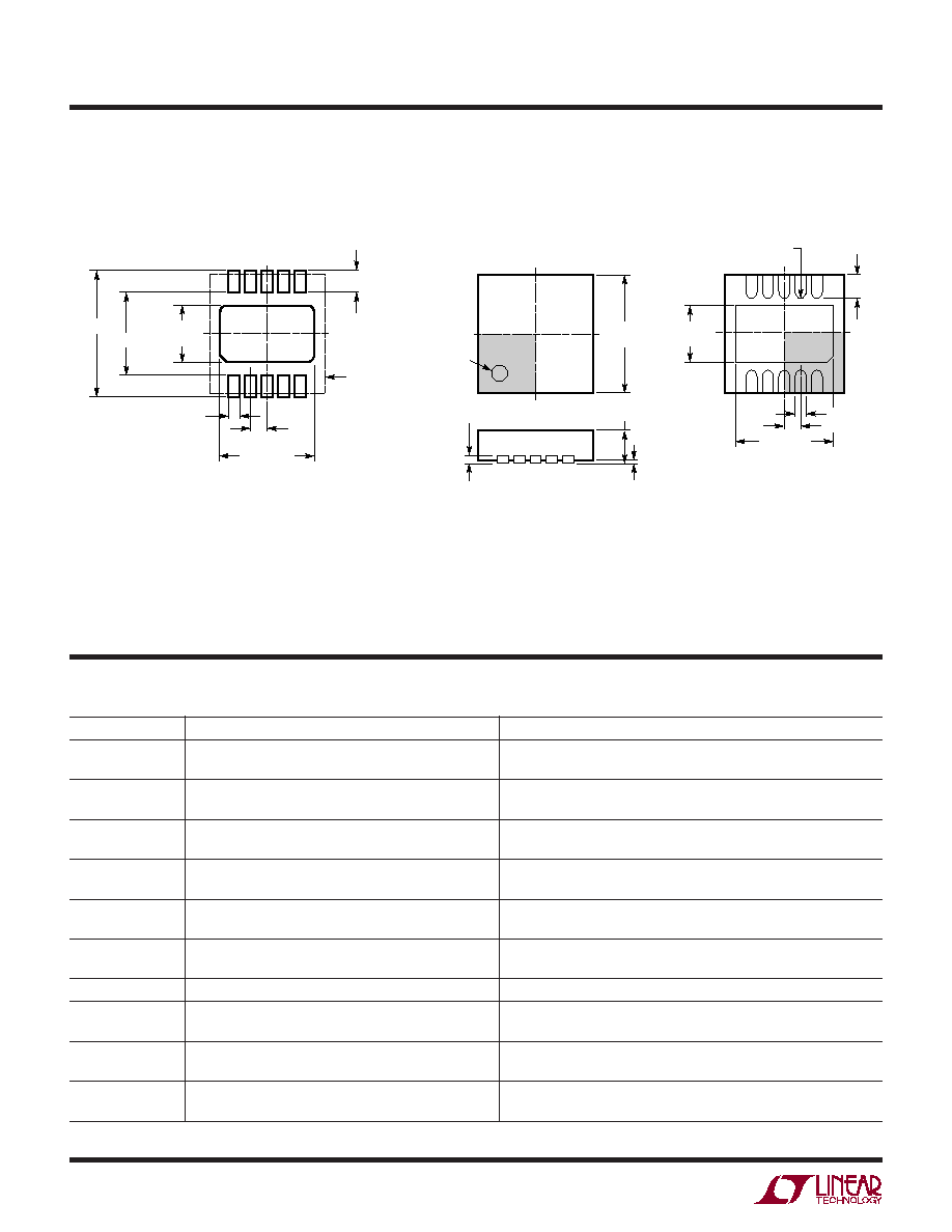
PACKAGE DESCRIPTIO
U
3.00
Ý0.10
(4 SIDES)
NOTE:
1. DRAWING TO BE MADE A JEDEC PACKAGE OUTLINE M0-229 VARIATION OF (WEED-2).
CHECK THE LTC WEBSITE DATA SHEET FOR CURRENT STATUS OF VARIATION ASSIGNMENT
2. DRAWING NOT TO SCALE
3. ALL DIMENSIONS ARE IN MILLIMETERS
4. DIMENSIONS OF EXPOSED PAD ON BOTTOM OF PACKAGE DO NOT INCLUDE
MOLD FLASH. MOLD FLASH, IF PRESENT, SHALL NOT EXCEED 0.15mm ON ANY SIDE
5. EXPOSED PAD SHALL BE SOLDER PLATED
6. SHADED AREA IS ONLY A REFERENCE FOR PIN 1 LOCATION ON THE
TOP AND BOTTOM OF PACKAGE
0.38
Ý 0.10
BOTTOM VIEW--EXPOSED PAD
1.65
Ý 0.10
(2 SIDES)
0.75
Ý0.05
R = 0.115
TYP
2.38
Ý0.10
(2 SIDES)
1
5
10
6
PIN 1
TOP MARK
(SEE NOTE 6)
0.200 REF
0.00 Ù 0.05
(DD10) DFN 1103
0.25
Ý 0.05
2.38
Ý0.05
(2 SIDES)
RECOMMENDED SOLDER PAD PITCH AND DIMENSIONS
1.65
Ý0.05
(2 SIDES)
2.15
Ý0.05
0.50
BSC
0.675
Ý0.05
3.50
Ý0.05
PACKAGE
OUTLINE
0.25
Ý 0.05
0.50 BSC
DD Package
10-Lead Plastic DFN (3mm
æ 3mm)
(Reference LTC DWG # 05-08-1699)