
1
LTC1536
Precision Triple Supply Monitor
for PCI Applications
1
2
3
4
8
7
6
5
V
CC3
V
CC5
V
CCA
GND
PBR
SRST
RST
RST
LTC1536
PUSHBUTTON
RESET
PCI
LOCAL
BUS
R
PU
SELECTED TO MEET RISE TIME
SLEW RATE REQUIREMENTS (1k MIN)
5V
±
5%
3.3V
±
0.3V
0.1
µ
F
R
PU
RST
1536 TA01
PWR GOOD
0.1
µ
F
Motherboard PCI RST Generation
TIME (20ns/DIV)
VOLTAGE (1V/DIV)
5
4
3
2
1
0
1536 TA02
V
CC5
= 5V TO 3V STEP
V
CC3
= V
CCA
= 3.3V
4.7k PULL-UP FROM
RST TO V
CC3
RST
V
CC5
Power Fail Waveform
5V Dropping Below 3.3V by 300mV
s
Simultaneously Monitors 5V, 3.3V and
Adjustable Inputs
s
Guaranteed Threshold Accuracy:
±
0.75%
s
Low Supply Current: 100
µ
A
s
Internal Reset Time Delay: 200ms
s
Manual Pushbutton Reset Input
s
Active Low and Active High Reset Outputs
s
Active Low "Soft" Reset Output
s
Power Supply Glitch Immunity
s
Guaranteed Reset for Either V
CC3
1V or V
CC5
1V
s
Meets PCI t
FAIL
Timing Specifications Rev 2.1
s
8-Pin SO and MSOP Packages
The LTC
®
1536 is designed for PCI local bus applications
with multiple supply voltages that require low power,
small size, high speed and high accuracy supply
monitoring.
For 3.3V and 5V supplies that are > 500mV below spec or
for the condition when the 5V supply falls below the 3.3V
supply, the LTC1536 has a very fast response time capable
of meeting the PCI t
FAIL
timing specification. Tight 0.75%
threshold accuracy and glitch immunity ensure reliable
reset operation without false triggering.
The RST output is guaranteed to be in the correct state for
V
CC5
or V
CC3
down to 1V. The 100
µ
A typical supply current
makes the LTC1536 ideal for power-conscious systems.
A manual pushbutton reset input provides the ability to
generate a very narrow "soft" reset pulse (100
µ
s typ) or a
200ms reset pulse equivalent to a power-on reset. Both
SRST and RST outputs are open-drain and can be OR-tied
with other reset sources.
s
PCI-Based Systems
s
Desktop Computers
s
Notebook Computers
s
Intelligent Instruments
s
Portable Battery-Powered Equipment
s
Network Servers
, LTC and LT are registered trademarks of Linear Technology Corporation.
DESCRIPTIO
U
FEATURES
APPLICATIO S
U
TYPICAL APPLICATIO
U
2
LTC1536
A
U
G
W
A
W
U
W
A
R
BSOLUTE
XI
TI
S
(Notes 1, 2)
Terminal Voltage
V
CC3
, V
CC5
, V
CCA
.................................... 0.3V to 7V
RST, SRST ............................................ 0.3V to 7V
RST ......................................... 0.3V to V
CC3
+ 0.3V
PBR .......................................................... 7V to 7V
Operating Temperature Range
LTC1536C .............................................. 0
°
C to 70
°
C
LTC1536I ............................................ 40
°
C to 85
°
C
Storage Temperature Range ................ 65
°
C to 150
°
C
Lead Temperature (Soldering, 10 sec)................. 300
°
C
W
U
U
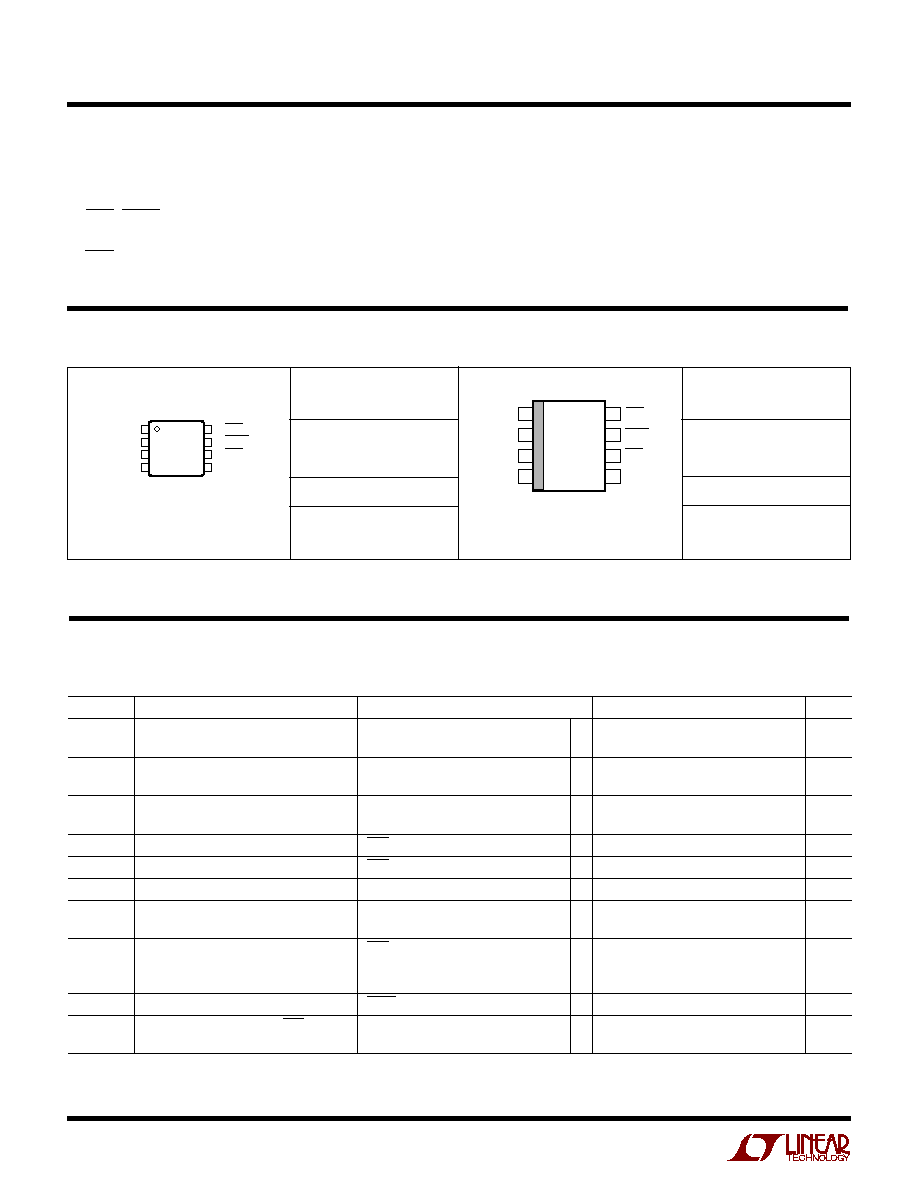
PACKAGE/ORDER I FOR ATIO
ORDER
PART NUMBER
ORDER
PART NUMBER
LTC1536CMS8
1
2
3
4
8
7
6
5
TOP VIEW
S8 PACKAGE
8-LEAD PLASTIC SO
V
CC3
V
CC5
V
CCA
GND
PBR
SRST
RST
RST
T
JMAX
= 125
°
C,
JA
= 150
°
C/ W
1
2
3
4
V
CC3
V
CC5
V
CCA
GND
8
7
6
5
PBR
SRST
RST
RST
TOP VIEW
MS8 PACKAGE
8-LEAD PLASTIC MSOP
T
JMAX
= 125
°
C,
JA
= 160
°
C/ W
MS8 PART MARKING
LTBV
Consult factory for Military grade parts.
SYMBOL
PARAMETER
CONDITIONS
MIN
TYP
MAX
UNITS
V
RT3
Reset Threshold V
CC3
0
°
C
T
A
70
°
C
q
2.962
2.985
3.000
V
40
°
C
T
A
85
°
C
q
2.925
2.985
3.008
V
V
RT5
Reset Threshold V
CC5
0
°
C
T
A
70
°
C
q
4.687
4.725
4.750
V
40
°
C
T
A
85
°
C
q
4.625
4.725
4.762
V
V
RTA
Reset Threshold V
CCA
0
°
C
T
A
70
°
C
q
0.992
1.000
1.007
V
40
°
C
T
A
85
°
C
q
0.980
1.000
1.007
V
V
CC
V
CC3
or V
CC5
Operating Voltage
RST in Correct Logic State
q
1
7
V
I
VCC3
V
CC3
Supply Current
PBR = V
CC3
q
100
200
µ
A
I
VCC5
V
CC5
Input Current
V
CC5
= 5V
q
10
20
µ
A
I
VCCA
V
CCA
Input Current
V
CCA
= 1V, 0
°
C
T
A
70
°
C
q
5
0
5
nA
V
CCA
= 1V, 40
°
C
T
A
85
°
C
q
15
0
15
nA
t
RST
Reset Pulse Width
RST Low with 10k
Pull-Up to V
CC3
0
°
C to 70
°
C
q
140
200
280
ms
40
°
C to 85
°
C
q
140
200
300
ms
t
SRST
Soft Reset Pulse Width
SRST Low with 10k
Pull-Up to V
CC3
q
50
100
200
µ
s
t
UV
V
CC
Undervoltage Detect to RST
V
CC5
, V
CC3
or V
CCA
Less Than Reset
13
µ
s
Threshold V
RT
by 1%
ELECTRICAL CHARACTERISTICS
V
CC3
= 3.3V, V
CC5
= 5V, V
CCA
= V
CC3
, T
A
= 25
°
C unless otherwise noted.
S8 PART MARKING
1536
1536I
LTC1536CS8
LTC1536IS8

3
LTC1536
SYMBOL
PARAMETER
CONDITIONS
MIN
TYP
MAX
UNITS
I
PBR
PBR Pull-Up Current
PBR = 0V, 0
°
C
T
A
70
°
C
q
3
7
10
µ
A
PBR = 0V, 40
°
C
T
A
85
°
C
q
3
7
15
µ
A
V
IL
PBR, RST Input Low Voltage
q
0.8
V
V
IH
PBR, RST Input High Voltage
q
2
V
t
PW
PBR Min Pulse Width
q
40
ns
t
DB
PBR Debounce
Deassertion of PBR Input to SRST
q
20
35
ms
Output (PBR Pulse Width = 1
µ
s)
t
PB
PBR Assertion Time for Transition
PBR Held Less Than V
IL
, 0
°
C to 70
°
C
q
1.4
2.0
2.8
s
from Soft to Hard Reset Mode
PBR Held Less Than V
IL
, 40
°
C to 85
°
C
q
1.4
2.0
3.0
s
V
OL
RST Output Voltage Low
I
SINK
= 5mA
q
0.15
0.4
V
I
SINK
= 100
µ
A
V
CC3
= 1V, V
CC5
= 0V
q
0.05
0.4
V
0
°
C
T
A
70
°
C
V
CC3
= 0V, V
CC5
= 1V
q
0.05
0.4
V
V
CC3
= 1V, V
CC5
= 1V
q
0.05
0.4
V
I
SINK
= 100
µ
A
V
CC3
= 1.1V, V
CC5
= 0V
q
0.05
0.4
V
40
°
C
T
A
85
°
C
V
CC3
= 0V, V
CC5
= 1.1V
q
0.05
0.4
V
V
CC3
= 1.1V, V
CC5
= 1.1V
q
0.05
0.4
V
SRST Output Voltage Low
I
SINK
= 2.5mA
q
0.15
0.4
V
RST Output Voltage Low
I
SINK
= 2.5mA
q
0.15
0.4
V
V
OH
RST Output Voltage High (Note 3)
I
SOURCE
= 1
µ
A
q
V
CC3
1
V
SRST Output Voltage High (Note 3)
I
SOURCE
= 1
µ
A
q
V
CC3
1
V
RST Output Voltage High
I
SOURCE
= 600
µ
A
q
V
CC3
1
V
t
PHL
Propagation Delay RST to RST
C
RST
= 20pF
25
ns
High Input to Low Output
t
PLH
Propagation Delay RST to RST
C
RST
= 20pF
45
ns
Low Input to High Output
t
FAIL
V
CC5
or V
CC3
0.5V Undervoltage
V
CC5
Drops Below 4.25V or V
CC3
Drops
q
150
450
ns
to RST (Note 4)
Below 2.5V (Note 5)
t
PF
V
CC5
< (V
CC3
300mV) RST (Note 4)
V
CC5
Drops Below V
CC3
By 300mV
q
50
90
ns
(Note 6)
ELECTRICAL CHARACTERISTICS
V
CC3
= 3.3V, V
CC5
= 5V, V
CCA
= V
CC3
, T
A
= 25
°
C unless otherwise noted.
Note 4: Conforms to PCI Local Bus Specification Rev 2.1,
Sect. 4.3.2 for t
FAIL
.
Note 5: V
CC3
or V
CC5
falling at 0.1V/
µ
s, time measured from
V
RTX
500mV to RST at 1.5V.
Note 6: V
CC5
falling from 5V to 3V in
10ns, time measured from
V
CC5
= (V
CC3
300mV) to RST at 1.5V.
The
q
denotes specifications which apply over the full operating
temperature range.
Note 1: Absolute Maximum Ratings are those values beyond which the life
of the device may be impaired.
Note 2: All voltage values are with respect to GND.
Note 3: The output pins SRST and RST have weak internal pull-ups to
V
CC3
of 6
µ
A. However, external pull-up resistors may be used when faster
rise times are required.
4
LTC1536
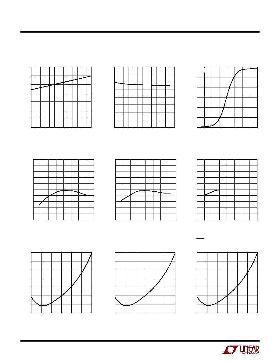
TYPICAL PERFOR
M
A
N
CE CHARACTERISTICS
U
W
V
CCA
Input Current
vs Input Voltage
TEMPERATURE (
°
C)
45
0
I
VCC3
(
µ
A)
20
40
60
80
140
120
5
35
55
1536 G01
100
25
15
75
I
VCC3
vs Temperature
INPUT VOLTAGE (V)
0.8
3
INPUT CURRENT (nA)
2
1
0
1
0.9
1.0
1.1
1.2
1536 G03
2
3
0.85
0.95
1.05
1.15
T
A
= 25
°
C
TEMPERATURE (
°
C)
45
0
I
VCC5
(
µ
A)
2.5
5.0
7.5
10.0
20.0
15.0
5
35
55
1536 G02
17.5
12.5
25
15
75
I
VCC5
vs Temperature
TEMPERATURE (
°
C)
60
V
CC5
THRESHOLD VOLTAGE, V
RT5
(V)
4.750
4.745
4.740
4.735
4.730
4.725
4.720
4.715
4.710
4.705
4.700
20
20
40
1536 G04
40
0
60
80
100
V
CC5
Threshold Voltage
vs Temperature
V
CCA
Threshold Voltage
vs Temperature
TEMPERATURE (
°
C)
60
V
CCA
THRESHOLD VOLTAGE, V
RTA
(V)
1.005
1.004
1.003
1.002
1.001
1.000
0.999
0.998
0.997
0.996
0.995
20
20
40
1536 G06
40
0
60
80
100
V
CC3
Threshold Voltage
vs Temperature
TEMPERATURE (
°
C)
60
V
CC3
THRESHOLD VOLTAGE, V
RT3
(V)
60
1536 G05
20
20
40
80
0
40
100
3.010
3.005
3.000
2.995
2.990
2.985
2.980
2.975
2.970
2.965
2.960
PBR Assertion Time to Reset
vs Temperature
Reset Pulse Width
vs Temperature
TEMPERATURE (
°
C)
50
210
215
220
25
75
1536 G07
205
200
25
0
50
100
195
190
RESET PULSE WIDTH, t
RST
(ms)
225
"Soft" Reset Pulse Width
vs Temperature
TEMPERATURE (
°
C)
50
105.0
107.5
110.0
25
75
1536 G08
102.5
100.0
25
0
50
100
97.5
95.0
SOFT RESET PULSE WIDTH, t
SRST
(
µ
s)
112.5
TEMPERATURE (
°
C)
50
2.10
2.15
2.20
25
75
1536 G09
2.05
2.00
25
0
50
100
1.95
1.90
PBR ASSERTION TIME TO RESET, t
PB
(SEC)
2.25

5
LTC1536
TYPICAL PERFOR
M
A
N
CE CHARACTERISTICS
U
W
V
CC3
Typical Transient Duration
vs Reset Comparator Overdrive
V
CCA
Typical Transient Duration
vs Reset Comparator Overdrive
V
CC3
RESET COMPARATOR OVERDRIVE, V
RT3
V
CC3
(V)
0.001
20
TYPICAL TRANSIENT DURATION (
µ
s)
30
40
45
50
0.01
0.1
1
1536 G10
10
0
25
35
15
5
RESET OCCURS
ABOVE CURVE
V
CCA
RESET COMPARATOR OVERDRIVE, V
RTA
V
CCA
(V)
0.001
20
TYPICAL TRANSIENT DURATION (
µ
s)
30
40
0.01
0.1
1
1536 G12
10
0
25
35
15
5
RESET OCCURS
ABOVE CURVE
V
CC5
Typical Transient Duration
vs Reset Comparator Overdrive
V
CC5
RESET COMPARATOR OVERDRIVE, V
RT5
V
CC5
(V)
0.001
20
TYPICAL TRANSIENT DURATION (
µ
s)
30
40
45
0.01
0.1
1
1536 G11
10
0
25
35
15
5
RESET OCCURS
ABOVE CURVE
RST Output Voltage
vs Supply Voltage
SUPPLY VOLTAGE, V
CC
(V)
0
RST OUTPUT VOLTAGE (V)
3.0
4.0
5.0
4.0
1536 G13
2.0
1.0
2.5
3.5
4.5
1.5
0.5
0
1.0
2.0
3.0
0.5
4.5
1.5
2.5
3.5
5.0
V
CC5
= V
CC3
= V
CCA
4.7k PULL-UP FROM RST TO V
CC5
T
A
= 25
°
C
Undervoltage Response Time
vs Temperature
TIME (1
µ
s/DIV)
VOLTAGE (500mV/DIV)
1536 G15
V
CC3
85
°
40
°
RST
MARGIN
DEVICE THRESHOLD
PCI SPEC
25
°
t
FAIL
SPEC
V
CC3
FALLING
FROM 3.3V TO
2.3V AT ( 0.1V/
µ
s)
RST Output Voltage
vs Supply Voltage
SUPPLY VOLTAGE, V
CC
(V)
0
RST OUTPUT VOLTAGE (V)
3.0
4.0
5.0
4.0
1536 G16
2.0
1.0
2.5
3.5
4.5
1.5
0.5
0
1.0
2.0
3.0
0.5
4.5
1.5
2.5
3.5
5.0
V
CC5
= V
CC3
= V
CCA
RST PIN LOADED WITH
10M
TO GND
T
A
= 25
°
C
Power-Fail Response Time
vs Temperature
TIME (20ns/DIV)
VOLTAGE (1V/DIV)
1536 G14
V
CC5
RST
85
°
40
°
25
°
6
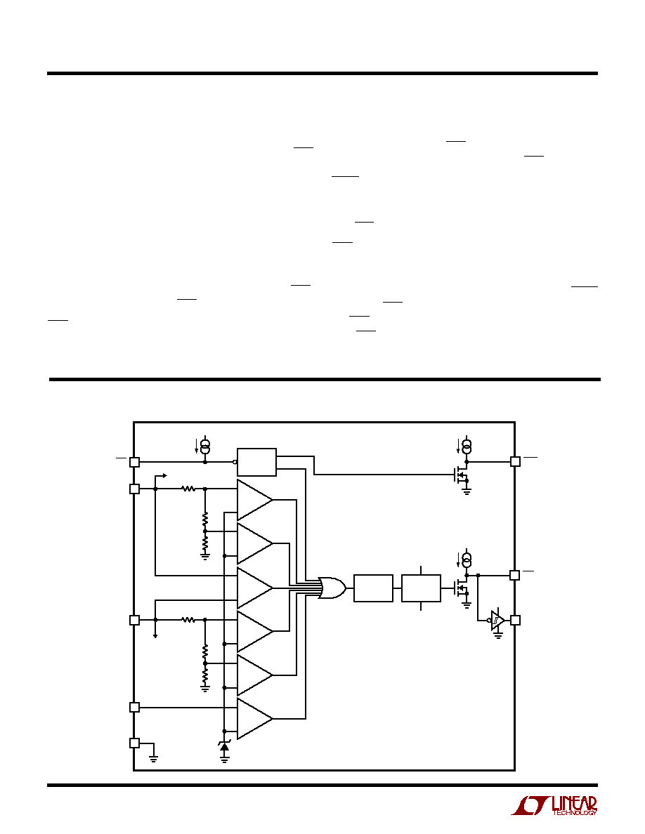
LTC1536
PI
N
FU
N
CTIO
N
S
U
U
U
V
CC3
(Pin 1): 3.3V Sense Input and Power Supply Pin for
the IC. Bypass to ground with
0.1
µ
F ceramic capacitor.
V
CC5
(Pin 2): 5V Sense Input. Used as gate drive for RST
output FET when the voltage on V
CC5
is greater than the
voltage on V
CC3
.
V
CCA
(Pin 3): 1V Sense, High Impedance Input. Can be
used as a logic input with a 1V threshold. If unused it can
be tied to either V
CC3
or V
CC5
.
GND (Pin 4): Ground.
RST (Pin 5): Reset Logic Output. Active high CMOS logic
output, drives high to V
CC3
, buffered compliment of RST.
An external pull-down on the RST pin will drive this pin high.
RST (Pin 6): Reset Logic Output. Active low, open-drain
logic output with weak pull-up to V
CC3
. Can be pulled up
greater than V
CC3
when interfacing to 5V logic.
V
CC3
SOFT RESET
RESET
3
V
CCA
2
V
CC5
TO
POWER
DETECT
8
PBR
7
SRST
4
GND
REF
PBR
TIMER
200ms
RESET
GENERATOR
POWER
DETECT/
GATE DRIVE
V
CC3
6
RST
5
V
CC3
V
CC3
V
CC5
RST
6
µ
A
V
CC3
7
µ
A
6
µ
A
+
FAST
+
FAST
+
SLOW
+
FAST
+
SLOW
+
SLOW
1
V
CC3
TO POWER DETECT
AND V
CC
INTERNAL
1326 BD
BLOCK DIAGRA
M
W
Asserted when one or more of the supplies are below trip
thresholds and held for 200ms after all supplies become
valid. Also asserted after PBR is held low for more than two
seconds and for an additional 200ms after PBR is released.
SRST (Pin 7): "Soft" Reset. Active low, open-drain logic
output with weak pull-up to V
CC3
. Can be pulled up greater
than V
CC3
when interfacing to 5V logic. Asserted for 100
µ
s
after PBR is held low for less than two seconds and released.
PBR (Pin 8): Pushbutton Reset. Active low logic input with
weak pull-up to V
CC3
. Can be pulled up greater than V
CC3
when interfacing to 5V logic. When asserted for less than
two seconds, outputs a soft reset 100
µ
s pulse on the SRST
pin. When PBR is asserted for greater than two seconds,
the RST output is forced low and remains low until 200ms
after PBR is released.
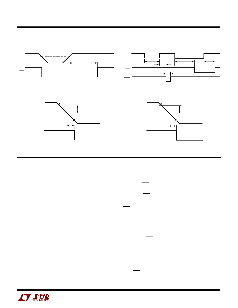
7
LTC1536
TI I G DIAGRA S
W
W
U
V
CC
Monitor Timing
Pushbutton Reset Function Timing
t < t
PB
t
PB
t
RST
t
DB
t
SRST
1536 TD02
PBR
RST
SRST
t
RST
1536 TD01
V
RTX
V
CCX
RST
t
FAIL
Fast Undervoltage Detect
t
FAIL
500mV
1536 TD03
V
CC3 OR
V
CC5
V
RTX
SLEW RATE
0.1V/
µ
s
RST
t
PF
300mV
1536 TD04
V
CC5
FALL TIME
10ns, V
CC3
= 3.3V
RST
3.3V
Power-Fail Detect
APPLICATIO
N
S I
N
FOR
M
ATIO
N
W
U
U
U
Operation
The LTC1536 is a low power, high accuracy triple supply
monitoring circuit. This reset generator has two basic
functions: generation of a reset when power supplies are
out of range, and generation of a reset or "soft" reset when
the reset button is pushed. The LTC1536 has the added
feature that when the reset supplies are grossly undervolt-
age there is a very short delay from undervoltage detect to
assertion of RST.
Supply Monitoring
All three V
CC
inputs must be above predetermined thresh-
olds for 200ms before the reset output is released. The
LTC1536 will assert reset during power-up, power-down
and brownout conditions on any one or more of the V
CC
inputs.
On power-up, either the V
CC5
or V
CC3
pin can power the
drive circuits for the RST pin. This ensures that RST will
be low when either V
CC5
or V
CC3
reaches 1V. As long as
any one of the V
CC
inputs is below its predetermined
threshold, RST will stay a logic low. Once all of the V
CC
inputs rise above their thresholds, an internal timer is
started and RST is released after 200ms. RST outputs the
inverted state of what is seen on RST.
RST is reasserted whenever any one of the V
CC
inputs
drops below its predetermined threshold and remains
asserted until 200ms after all of the V
CC
inputs are above
their thresholds.
On power-down, once any of the V
CC
inputs drops below
its threshold, RST is held at a logic low. A logic low of 0.4V
is guaranteed until V
CC3
and V
CC5
drops below 1V.
Pushbutton Reset
The LTC1536 provides a pushbutton reset input pin. The
PBR input has an internal pull-up current source to V
CC3
.
If the PBR pin is not used it can be left floating.

8
LTC1536
When the PBR is pulled low for less than t
PB
(
2 sec), a
narrow (100
µ
s typ) soft reset pulse is generated on the
SRST output pin after the button is released. The push-
button circuitry contains an internal debounce counter
which delays the output of the soft reset pulse by typically
20ms. This pin can be OR-tied to the RST pin and issue
what is called a "soft" reset. The SRST thereby resets the
microprocessor without interrupting the DRAM refresh
cycle. In this manner DRAM information remains undis-
turbed. Alternatively, SRST may be monitored by the
processor to initiate a software-controlled reset.
When the PBR pin is held low for longer than t
PB
(
2 sec),
a standard reset is generated. Once the 2-second period
has elapsed, a reset signal is produced by the pushbutton
logic, thereby clearing the reset counter. Once the PBR
pin is released, the reset counter begins counting the
reset period (200ms nominal). Consequently, the reset
outputs remain asserted for approximately 200ms after
the button is released.
Fast Undervoltage for PCI Applications
The LTC1536 is designed for PCI Local Bus applications
that require reset to be asserted quickly in response to one
or both of the power supply rails (5V and 3.3V) going out
of spec. The spec for t
FAIL
and t
PF
are met with enough
margin to give the designer the ability to add follow-on
logic as needed by system requirements. The V
CCA
pin can
be used to monitor the "power good" signal and keep reset
applied until both supplies are in spec and the power good
signal is high.
Glitch Immunity and Fast Undervoltage Detection
The LTC1536 achieves its high speed characteristics while
maintaining glitch immunity by using two sets of com-
parators. The V
CC5
and V
CC3
sense inputs each have two
comparators set at different thresholds. A slow, very
accurate comparator monitors the supply for precision
undervoltage detection. In parallel, but with a threshold
250mV lower than the precision threshold, is a very fast
comparator that detects when the supply is quickly going
out of specification. Because the fast comparator thresh-
old is set 250mV above the PCI specification, typical
values for t
FAIL
can be negative.
3V or 5V Power Detect/Gate Drive
The LTC1536 for the most part is powered internally from
the V
CC3
pin. The exception is at the gate drive of the output
FET on the RST pin. On the gate to this FET is power detect
circuitry used to detect and drive the gate from either the
3.3V pin or the 5V pin, whichever pin has the highest
potential. This ensures the part pulls the RST pin low as
soon as either input pin is
1V.
Extended ESD Tolerance of the PBR Input Pin
The PBR pin is susceptible to ESD since it can be brought
out to a front panel in normal applications. The ESD
tolerance of this pin can be increased by adding a resistor
in series with the PBR pin. A 10k resistor can increase the
ESD tolerance of the PBR pin to approximately 10kV. The
PBR's internal pull-up current of 7
µ
A typical means there
is only 70mV (150mV max) dropped across the resistor.
APPLICATIO
N
S I
N
FOR
M
ATIO
N
W
U
U
U
TYPICAL APPLICATIO
N
S
N
U
1
2
3
4
8
7
6
5
V
CC3
V
CC5
V
CCA
GND
PBR
SRST
RST
RST
LTC1536
PCI
LOCAL
BUS
0.1
µ
F
3.3V SUPPLY
RESET
5V SUPPLY
1536 TA08
0.1
µ
F
ONBOARD
DEVICE
PCI Expansion Board RST Generation
Dual Supply Monitor (3.3V and 5V, V
CCA
Input
Monitoring "Power Good")
1
2
3
4
8
7
6
5
V
CC3
V
CC5
V
CCA
GND
PBR
SRST
RST
RST
LTC1536
3.3V
SYSTEM RESET
5V
PWR GOOD
1536 TA04

9
LTC1536
TYPICAL APPLICATIO
N
S
N
U
Triple Supply Monitor (3.3V, 5V and Adjustable)
1
2
3
4
8
7
6
5
V
CC3
V
CC5
V
CCA
GND
PBR
SRST
RST
RST
LTC1536
3.3V
SYSTEM RESET
100k
5V
1536 TA09
1
2
3
4
8
7
6
5
V
CC3
V
CC5
V
CCA
GND
PBR
SRST
RST
RST
LTC1536
3.3V
SYSTEM RESET
*OPTIONAL RESISTOR EXTENDS
ESD TOLERANCE OF PBR INPUT
8kV TO 10kV
5V
R2
R1
1536 TA03
ADJUSTABLE SUPPLY
OR DC/DC FEEDBACK
DIVIDER
10k*
PUSHBUTTON
RESET
SRST Tied to RST and OR-Tying Other Sources to RST to
Generate Reset and Reset
4.7k
SRST
6
µ
A
6
µ
A
3.3V
LTC1536
PUSHBUTTON
RESET
RESET
1536 TA05
OTHER OPEN DRAIN
RESET SOURCES
OR-TIED TO RESET
7
8
PBR
RST
RST
V
CC3
6
5
1
2
3
4
8
7
6
5
V
CC3
V
CC5
V
CCA
GND
PBR
SRST
RST
RST
LTC1536
3.3V
SYSTEM RESET
5V
22.1k
1%
1536 TA07
35.7k
1%
LTC1435
ADJUSTABLE
RESET TRIP
THRESHOLD 2.74V
2.9V
2.8k
1%
6
V
OSENSE
Using V
CCA
Tied to DC/DC Feedback Divider
RESET Valid for V
CC3
Down to 0V
in a Dual Supply Application
10
LTC1536
Dimensions in inches (millimeters) unless otherwise noted.
PACKAGE DESCRIPTIO
N
U
MS8 Package
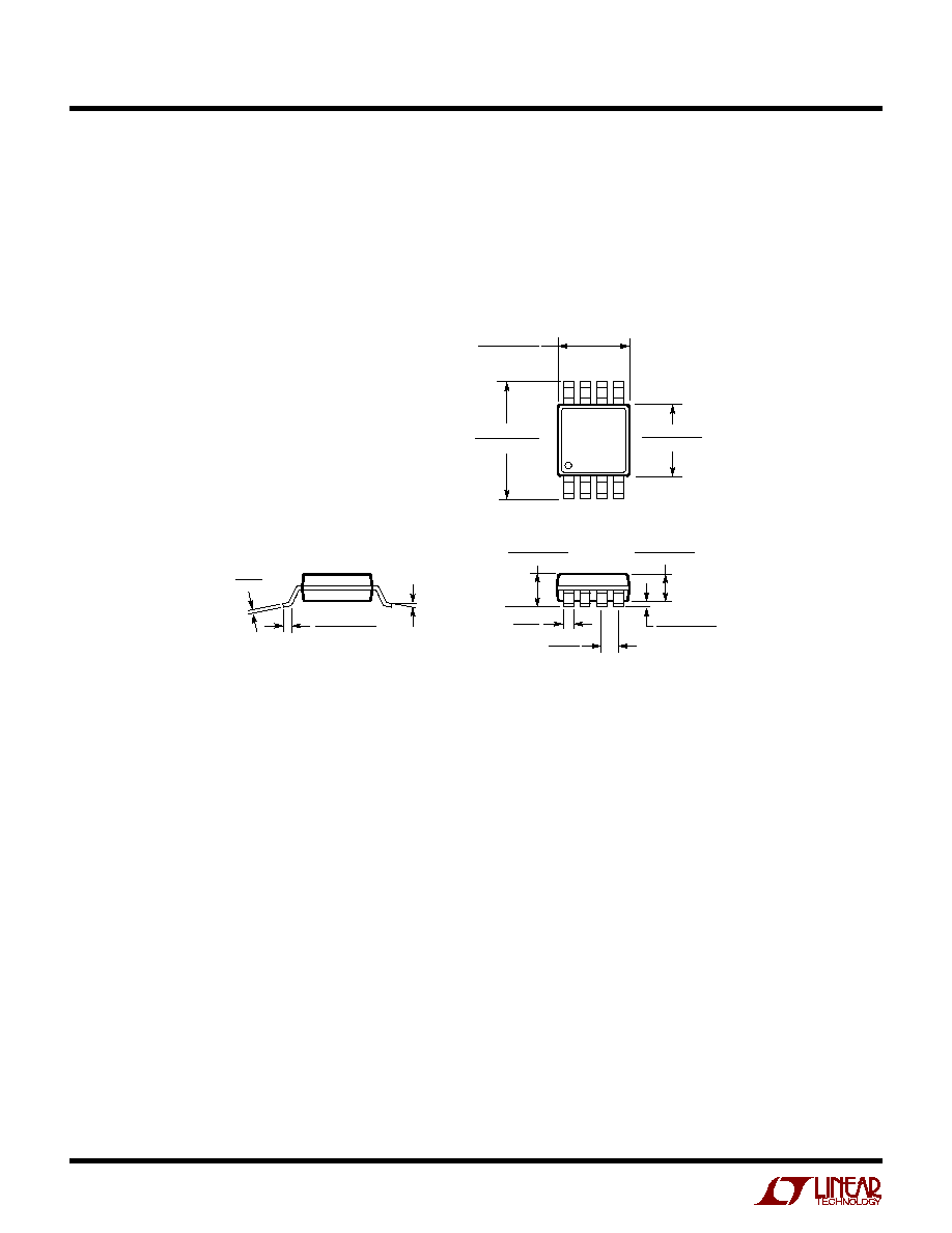
8-Lead Plastic MSOP
(LTC DWG # 05-08-1660)
MSOP (MS8) 1197
* DIMENSION DOES NOT INCLUDE MOLD FLASH, PROTRUSIONS OR GATE BURRS. MOLD FLASH,
PROTRUSIONS OR GATE BURRS SHALL NOT EXCEED 0.006" (0.152mm) PER SIDE
** DIMENSION DOES NOT INCLUDE INTERLEAD FLASH OR PROTRUSIONS.
INTERLEAD FLASH OR PROTRUSIONS SHALL NOT EXCEED 0.006" (0.152mm) PER SIDE
0.021
±
0.006
(0.53
±
0.015)
0
°
6
°
TYP
SEATING
PLANE
0.007
(0.18)
0.040
±
0.006
(1.02
±
0.15)
0.012
(0.30)
REF
0.006
±
0.004
(0.15
±
0.102)
0.034
±
0.004
(0.86
±
0.102)
0.0256
(0.65)
TYP
1
2
3
4
0.192
±
0.004
(4.88
±
0.10)
8
7 6
5
0.118
±
0.004*
(3.00
±
0.102)
0.118
±
0.004**
(3.00
±
0.102)
11
LTC1536
Dimensions in inches (millimeters) unless otherwise noted.
PACKAGE DESCRIPTIO
N
U
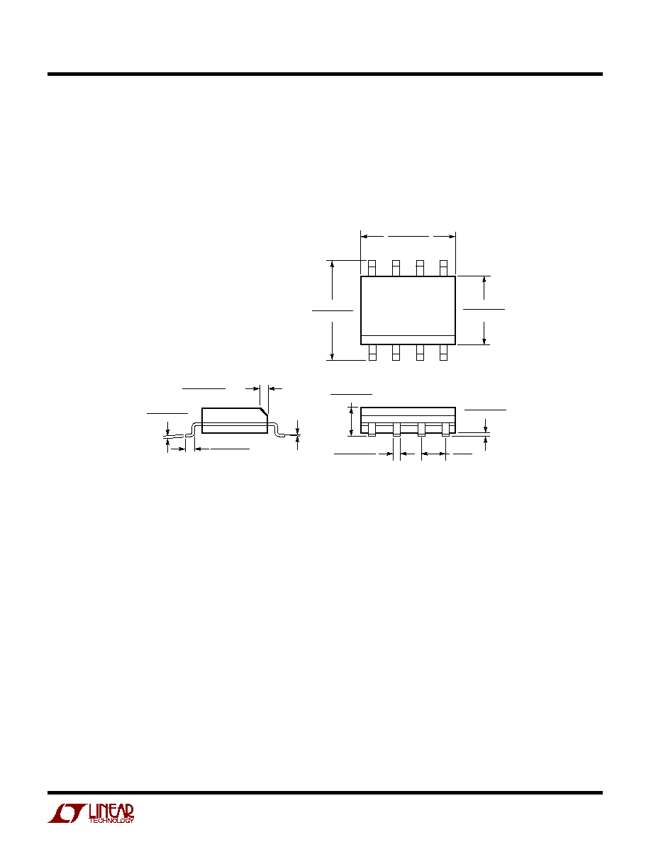
S8 Package
8-Lead Plastic Small Outline (Narrow 0.150)
(LTC DWG # 05-08-1610)
1
2
3
4
0.150 0.157**
(3.810 3.988)
8
7
6
5
0.189 0.197*
(4.801 5.004)
0.228 0.244
(5.791 6.197)
0.016 0.050
0.406 1.270
0.010 0.020
(0.254 0.508)
×
45
°
0
°
8
°
TYP
0.008 0.010
(0.203 0.254)
SO8 0996
0.053 0.069
(1.346 1.752)
0.014 0.019
(0.355 0.483)
0.004 0.010
(0.101 0.254)
0.050
(1.270)
TYP
DIMENSION DOES NOT INCLUDE MOLD FLASH. MOLD FLASH
SHALL NOT EXCEED 0.006" (0.152mm) PER SIDE
DIMENSION DOES NOT INCLUDE INTERLEAD FLASH. INTERLEAD
FLASH SHALL NOT EXCEED 0.010" (0.254mm) PER SIDE
*
**
Information furnished by Linear Technology Corporation is believed to be accurate and reliable.
However, no responsibility is assumed for its use. Linear Technology Corporation makes no represen-
tation that the interconnection of its circuits as described herein will not infringe on existing patent rights.

12
LTC1536
©
LINEAR TECHNOLOGY CORPORATION 1997
1536f, sn1536a LT/TP 0498 4K · PRINTED IN THE USA
TYPICAL APPLICATIO
N
S
N
U
Linear Technology Corporation
1630 McCarthy Blvd., Milpitas, CA 95035-7417
q
(408) 432-1900
FAX: (408) 434-0507
q
TELEX: 499-3977
q
www.linear-tech.com
PART NUMBER
DESCRIPTION
COMMENTS
LTC690
5V Supply Monitor, Watchdog Timer and Battery Backup
4.65V Threshold
LTC694-3.3
3.3V Supply Monitor, Watchdog Timer and Battery Backup
2.9V Threshold
LTC699
5V Supply Monitor and Watchdog Timer
4.65V Threshold
LTC1232
5V Supply Monitor, Watchdog Timer and Pushbutton Reset
4.37V/4.62V Threshold
LTC1326
Micropower Precision Triple Supply Monitor
4.725V, 3.118V, 1V Thresholds (
±
0.75%)
LTC1326-2.5
Micropower Precision Triple Supply Monitor
2.363V, 3.118V, 1V Thresholds (
±
0.75%)
RELATED PARTS
Quad Supply Monitor:
12V: Undervoltage, Overvoltage
5V: Undervoltage, Overvoltage
3.3V: Undervoltage, Overvoltage
12V: Undervoltage
+
+
+
+
A
PWR GOOD
B
2
12V
3
LTC1444
4
5
1
6
7
1.21M
1.21M
1%
2.37M
1%
3.3V
±
0.3V
5V
±
5%
12V
±
5%
12V
±
10%
1.05M
1%
102k
1%
100k
0.1
µ
F
OPTIONAL
1M
4.02M
1%
C
16
D
15
9
HYST
1536 TA07
11
10
12
13
8
14
9.31M
1%
1.21M
1%
REF
1.221V
10.7M
1%
5V
SYSTEM
RESET
1
2
3
4
8
7
6
5
V
CC3
V
CC5
V
CCA
GND
PBR
SRST
RST
RST
LTC1536