1
LTC1402
Serial 12-Bit, 2.2Msps
Sampling ADC with Shutdown
October 1999
FEATURES
DESCRIPTIO
N
U
s
Sample Rate: 2.2Msps
s
72dB S/(N + D) and 89dB THD at Nyquist
s
No Missing Codes over Temperature
s
Available in 16-Pin Narrow SSOP Package
s
Single Supply 5V or
±
5V Operation
s
Power Dissipation: 90mW (Typ)
s
Nap Mode with Instant Wake-Up: 15mW
s
Sleep Mode: 10
µ
W
s
True Differential Inputs Reject Common Mode Noise
s
80MHz Full Power Bandwidth Sampling
s
Input Range (1mV/LSB): 0V to 4.096V or
±
2.048V
s
Internal Reference Can Be Overdriven Externally
s
3-Wire Interface to DSPs and Processors (SPI and
MICROWIRE
TM
Compatible)
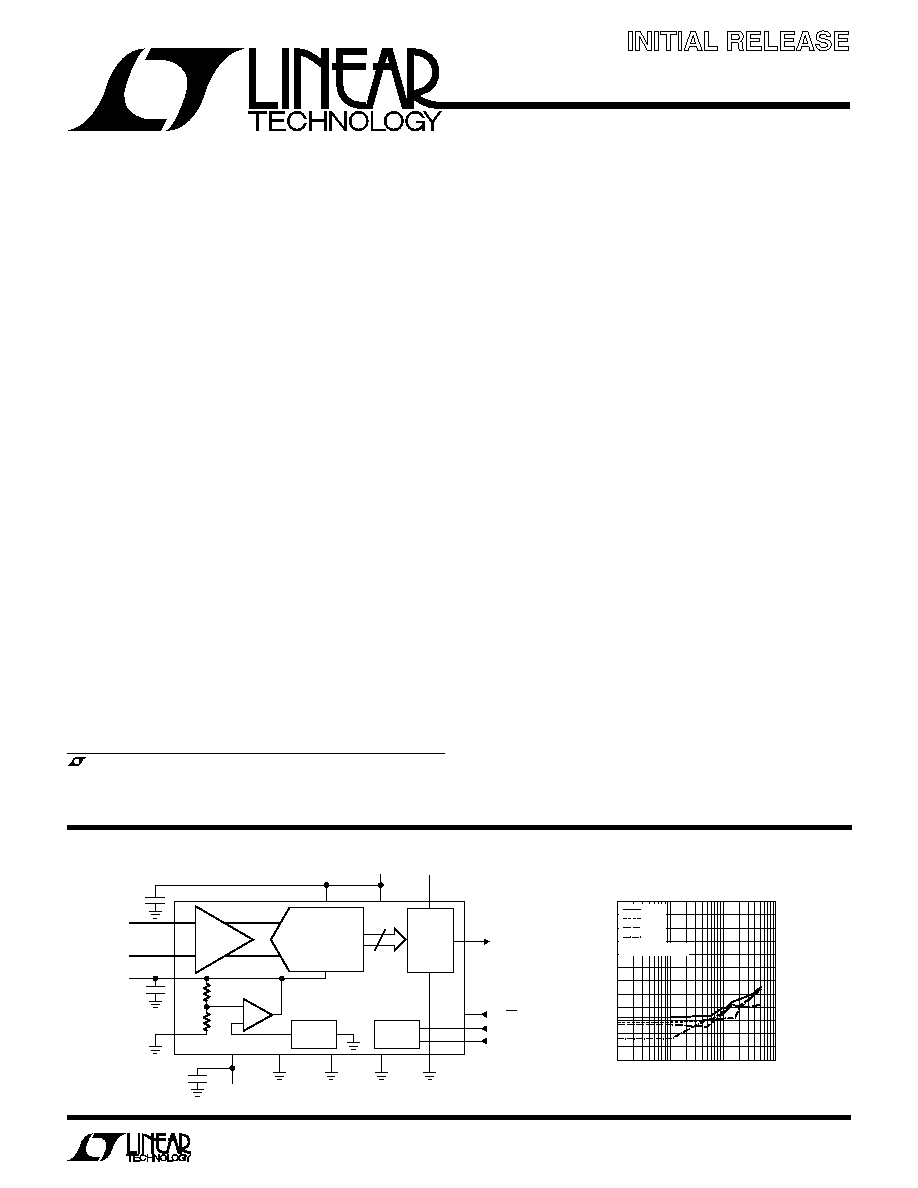
The LTC
®
1402 is a 12-bit, 2.2Msps sampling A/D con-
verter. This high performance device includes a high dy-
namic range sample-and-hold and a precision reference.
It operates from a single 5V supply or dual
±
5V supplies
and draws only 90mW from 5V.
The versatile differential input offers a unipolar range of
4.096V and a bipolar range of
±
2.048V for dual supply
systems where high performance op amps perform best,
eliminating the need for special translation circuitry.
The high common mode rejection allows users to elimi-
nate ground loops and common mode noise by measuring
signals differentially from the source.
Outstanding AC performance includes 72dB S/(N + D) and
93dB SFDR at the Nyquist input frequency of 1.1MHz
with dual
±
5V supplies and 84dB SFDR with a single 5V
supply.
The LTC1402 has two power saving modes: Nap and
Sleep. Nap mode consumes only 15mW of power and
Sleep can wake up and convert immediately. In Sleep
mode, it typically consumes 10
µ
W of power. Upon power-
up from Sleep mode, a reference ready (REFRDY) signal
is available in the serial data word to indicate that the
reference has settled and the chip is ready to convert.
The 3-wire serial port allows compact and efficient data
transfer to a wide range of microprocessors, microcon-
trollers and DSPs. A digital output driver power supply pin
allows direct connection to 3V or lower logic.
SAMPLE-
AND-HOLD
D
OUT
BIP/UNI
CONV
SCK
OV
DD
10
8
16
15
DV
DD
AV
DD
1
12
11
GAIN
7
5
4
3
5V OR 0V
10
µ
F
10
µ
F
V
REF
4.096V
10
µ
F
64k
OUTPUT
BUFFER
1402 TA01
2.048
REFERENCE
TIMING
LOGIC
+A
IN
LTC1402
OGND
9
6
2
DGND
A
IN
5V
3V OR 5V
AGND1
V
SS
14
13
AGND2
+
64k
12-BIT ADC
APPLICATIO
N
S
U
MICROWIRE is a trademark of National Semiconductor Corp.
, LTC and LT are registered trademarks of Linear Technology Corporation.
s
Telecommunications
s
High Speed Data and Signal Acquisition
s
Digitally Multiplexed Data Acquisition Systems
s
Digital Radio Receivers
s
Spectrum Analysis
s
Low Power and Battery-Operated Systems
s
Handheld or Portable Instruments
s
Imaging Systems
Information furnished by Linear Technology Corporation is believed to be accurate and reliable.
However, no responsibility is assumed for its use. Linear Technology Corporation makes no represen-
tation that the interconnection of its circuits as described herein will not infringe on existing patent rights.
Final Electrical Specifications
BLOCK DIAGRA
W
5 Harmonic THD, 2nd, 3rd and SFDR
vs Input Frequency (Unipolar)
INPUT FREQUENCY (Hz)
10
4
10
5
10
6
10
7
80
THD, SFDR, 2ND 3RD (dB)
60
40
1401 G05
100
120
0
20
90
70
50
110
10
30
THD
SFDR
2ND
3RD
f
SAMPLE
= 2.22MHz

2
LTC1402
PACKAGE/ORDER I
N
FOR
M
ATIO
N
W
U
U
ABSOLUTE
M
AXI
M
U
M
RATINGS
W
W
W
U
AV
DD
= DV
DD
= OV
DD
= V
DD
(Notes 1, 2)
Supply Voltage (V
DD
) ................................................. 6V
Negative Supply Voltage (V
SS
) ............................... 6V
Total Supply Voltage (V
DD
to V
SS
) .......................... 12V
Analog Input Voltage
(Note 3) .......................... (V
SS
0.3V) to (V
DD
+ 0.3V)
Digital Input Voltage
(Note 4) .......................... (V
SS
0.3V) to (V
DD
+ 0.3V)
Digital Output Voltage ......... (V
SS
0.3V) to (V
DD
+ 0.3V)
Power Dissipation .............................................. 250mW
Operation Temperature Range
LTC1402C ............................................... 0
°
C to 70
°
C
LTC1402I ............................................ 40
°
C to 85
°
C
Storage Temperature Range ................. 65
°
C to 150
°
C
Lead Temperature (Soldering, 10 sec).................. 300
°
C
ORDER PART
NUMBER
GN PART MARKING
1402
1402I
Consult factory for Military grade parts.
LTC1402CGN
LTC1402IGN
T
JMAX
= 125
°
C,
JA
= 150
°
C/ W
TOP VIEW
GN PACKAGE
16-LEAD NARROW PLASTIC SSOP
1
2
3
4
5
6
7
8
16
15
14
13
12
11
10
9
AV
DD
AGND1
A
IN
+
A
IN
V
REF
AGND2
GAIN
BIP/UNI
CONV
SCK
VSS
DGND
DV
DD
0V
DD
D
OUT
OGND
CO
N
VERTER CHARACTERISTICS
U
The
q
denotes the specifications which apply over the full operating
temperature range, otherwise specifications are at T
A
= 25
°
C. With internal reference (Note 5).
PARAMETER
CONDITIONS
MIN
TYP
MAX
UNITS
Resolution (No Missing Codes)
q
12
Bits
Integral Linearity Error
(Note 6)
q
±
0.35
±
1
LSB
Differential Linearity
(Note 6)
q
±
0.25
±
1
LSB
Offset Error
(Note 6)
q
±
2
±
10
LSB
Full-Scale Error
(Note 6)
q
±
10
±
15
LSB
Full-Scale Tempco
Internal Reference (Note 6)
±
15
ppm/
°
C
External Reference
±
1
ppm/
°
C
The
q
denotes the specifications which apply over the full operating temperature range,
otherwise specifications are at T
A
= 25
°
C. (Note 5)
SYMBOL
PARAMETER
CONDITIONS
MIN
TYP
MAX
UNITS
V
IN
Analog Differential Input Range (Notes 3, 11)
Bipolar Mode with BIP/UNI High
q
±
2.048
V
4.75V
V
DD
5.25V
V
5.25V
V
SS
4.75V
V
Unipolar Mode with BIP/UNI Low
q
0 to 4.096
V
4.75V
V
DD
5.25V
V
5.25V
V
SS
0V
V
V
CM
Analog Common Mode + Differential
Dual
±
5V Supply
2.5 to 5
V
Input Range (Note 12)
Single 5V Supply
0 to 5
V
I
IN
Analog Input Leakage Current
q
1
µ
A
C
IN
Analog Input Capacitance
10
pF
t
ACQ
Sample-and-Hold Acquisition Time
q
60
ns
t
AP
Sample-and-Hold Aperture Delay Time
2.6
ns
t
JITTER
Sample-and-Hold Aperture Delay Time Jitter
1
ps
CMRR
Analog Input Common Mode Rejection Ratio
f
IN
= 1MHz, V
IN
= 2V to 2V
62
dB
f
IN
= 100MHz, V
IN
= 2V to 2V
24
dB
A ALOG I PUT
U
U

3
LTC1402
The
q
denotes the specifications which apply over the full operating temperature range,
otherwise specifications are at T
A
= 25
°
C. Bipolar mode with
±
5V supplies and unipolar mode with 5V supply. (Note 5)
SYMBOL
PARAMETER
CONDITIONS
MIN
TYP
MAX
UNITS
S/(N + D)
Signal-to-Noise Plus
100kHz Input Signal
72.5
dB
Distortion Ratio
1.1MHz Input Signal
q
69
72.0
dB
THD
Total Harmonic
100kHz First 5 Harmonics, Bipolar Mode
89
dB
Distortion
1.1MHz First 5 Harmonics, Bipolar Mode
q
89
74.5
dB
100kHz First 5 Harmonics, Unipolar Mode
87
dB
1.1MHz First 5 Harmonics, Unipolar Mode
82
dB
SFDR
Spurious Free
1.1MHz Input Signal in Bipolar Mode
93
dB
Dynamic Range
1.1MHz Input Signal in Unipolar Mode
84
dB
IMD
Intermodulation
±
1V 1.25MHz into A
IN
+
, 1.2MHz into A
IN
Bipolar Mode
84
dB
Distortion
1.5V to 3.5V 1.25MHz into A
IN
+
, 1.2MHz into A
IN
Unipolar Mode
84
dB
Code-to-Code
V
REF
= 4.096V, 1LSB = 1mV
0.18
LSB
RMS
Transition Noise
Full Power Bandwidth
V
IN
= 4V
P-P
, D
OUT
= 2828
P-P
(Note 18)
82
MHz
Full Linear Bandwidth
S/(N + D)
68dB Bipolar Mode
5.0
MHz
Unipolar Mode
3.5
MHz
DY
N
A
M
IC ACCURACY
U
W
The
q
denotes the specifications which apply over the
full operating temperature range, otherwise specifications are at T
A
= 25
°
C. (Note 5)
I
N
TER
N
AL REFERE
N
CE CHARACTERISTICS
U
U
U
PARAMETER
CONDITIONS
MIN
TYP
MAX
UNITS
V
REF
Output Voltage
I
OUT
= 0
4.096
V
V
REF
Output Tempco
15
ppm/
°
C
V
REF
Line Regulation
AV
DD
= 4.75V to 5.25V, V
REF
= 4.096V
1
LSB/V
V
REF
Output Resistance
Load Current = 0.5mA
2
V
REF
Settling Time
2
ms
The
q
denotes the specifications which apply over the
full operating temperature range, otherwise specifications are at T
A
= 25
°
C. (Note 5)
SYMBOL
PARAMETER
CONDITIONS
MIN
TYP
MAX
UNITS
V
IH
High Level Input Voltage
V
DD
= 5.25V
q
2.4
V
V
IL
Low Level Input Voltage
V
DD
= 4.75V
q
0.8
V
I
IN
Digital Input Current
V
IN
= 0V to V
DD
q
±
10
µ
A
C
IN
Digital Input Capacitance
5
pF
V
OH
High Level Output Voltage
OV
DD
= 4.75V, I
OUT
= 10
µ
A
4.7
V
OV
DD
= 4.75V, I
OUT
= 200
µ
A
q
4
V
OV
DD
= 3V, I
OUT
= 200
µ
A
q
2.5
2.9
V
V
OL
Low Level Output Voltage
V
DD
= 4.75V, I
OUT
= 160
µ
A
0.05
V
V
DD
= 4.75V, I
OUT
= 1.6mA
q
0.10
0.4
V
I
OZ
Hi-Z Output Leakage D
OUT
V
OUT
= 0V to V
DD
q
±
10
µ
A
C
OZ
Hi-Z Output Capacitance D
OUT
15
pF
I
SOURCE
Output Short-Circuit Source Current
V
OUT
= 0V, OV
DD
= 5V
40
mA
V
OUT
= 0V, OV
DD
= 3V
15
mA
I
SINK
Output Short-Circuit Sink Current
V
OUT
= OV
DD
= 5V
40
mA
DIGITAL I PUTS A D DIGITAL OUTPUTS
U
U

4
LTC1402
SYMBOL
PARAMETER
CONDITIONS
MIN
TYP
MAX
UNITS
f
SAMPLE(MAX)
Maximum Sampling Frequency (Conversion Rate)
q
2.2
MHz
t
THROUGHPUT
Minimum Sampling Period (Conversion + Acquisiton Period)
q
455
ns
t
SCK
Minimum Clock Period
q
28
10000
ns
t
CONV
Conversion Time Greater Than 13 Clocks + 6ns
(Note 9)
q
375
ns
t
ACQ
Acquisition Time Greater Than 2 Clocks 6ns
(Notes 9, 16)
q
51
ns
t
1
Minimum Positive or Negative SCK Pulse Width
(Note 9)
q
3.8
6
ns
t
2
CONV to SCK
Setup Time
(Notes 9, 13)
q
7.3
12
ns
t
3
SCK
After CONV
(Note 9)
q
0
ns
t
4
Minimum Positive or Negative CONV Pulse Width
(Note 9)
q
3.5
5
ns
t
5
SCK
to Sample Mode
(Notes 9, 14)
q
9
14
ns
t
6
CONV to Hold Mode
(Note 9)
q
3.4
5
ns
t
7
Minimum Delay Between Conversions
(Note 9)
q
48
ns
t
8
Minimum Delay from SCK
to Valid Bits 0 Through 11
(Notes 9, 15)
q
9
12
ns
t
8a
Minimum Delay from SCK to Valid REFREADY
(Notes 9, 15)
q
15
20
ns
t
9
SCK to Hi-Z at D
OUT
(Notes 9, 15)
q
11.4
16
ns
t
10
Previous D
OUT
Bit Remains Valid After SCK
(Notes 9, 15)
q
4
7
ns
t
11
REFREADY Bit Delay After Sleep-to-Wake Transition
(Notes 9, 17)
q
10
ms
t
12
V
REF
Settling Time After Sleep-to-Wake Transition
(Notes 9, 17)
q
2
ms
The
q
denotes the specifications which apply over the full operating temperature
range, otherwise specifications are at T
A
= 25
°
C. (Note 5)
SYMBOL
PARAMETER
CONDITIONS
MIN
TYP
MAX
UNITS
V
DD
Positive Supply Voltage
4.75
5.00
5.25
V
V
SS
Negative Supply Voltage
5.25
5.00
0
V
I
DD
Positive Supply Current
Active Mode
q
18
30
mA
Nap Mode
q
3
5
mA
Sleep Mode
2
10
µ
A
I
SS
Negative Supply Current
Active, Sleep or Nap Modes with SCK Off
q
2
µ
A
PD
Power Dissipation
Active Mode with SCK in Fixed State (Hi or Lo)
90
150
mW
POWER REQUIRE E TS
W
U
Note 1: Absolute Maximum Ratings are those values beyond which the life
of a device may be impaired.
Note 2: All voltage values are with respect to ground with DGND, AGND1
and AGND2 wired together.
Note 3: When these pins are taken below V
SS
or above V
DD
, they will be
clamped by internal diodes. This product can handle input currents greater
than 100mA below V
SS
or greater than V
DD
without latchup.
Note 4: When these pins are taken below V
SS
, they will be clamped by
internal diodes. This product can handle input currents greater than
100mA below V
SS
or greater than V
DD
. These pins are not clamped to V
DD
.
Note 5: V
DD
= 5V, f
SAMPLE
= 2.2MHz, V
SS
= 0V for unipolar mode
specifications and V
SS
= 5V for bipolar specifications.
The
q
denotes the specifications which apply over the full operating temperature
range, otherwise specifications are at T
A
= 25
°
C. (Note 5)
Note 6: Linearity, offset and full-scale specifications apply for a single-
ended A
IN
+
input with A
IN
grounded and using the internal reference in
bipolar mode with
±
5V supplies.
Note 7: Integral linearity is defined as the deviation of a code from the
straight line passing through the actual endpoints of a transfer curve. The
deviation is measured from the center of quantization band.
Note 8: Bipolar offset is the offset measured from 0.5LSB when the input
flickers between 1000 0000 0000 and 0111 1111 1111.
Note 9: Guaranteed by design, not subject to test.
Note 10: Recommended operating conditions.
Note 11: The analog input range is defined as the voltage difference
between A
IN
+
and A
IN
. The bipolar
±
2.048V input range could be used
with a single 5V supply if the absolute voltages of the inputs remain within
the single 5V supply voltage.
TI I G CHARACTERISTICS
U
W

5
LTC1402
Note 12: The absolute voltage at A
IN
+
and A
IN
must be within this range.
Note 13: If less than 7.3ns is allowed, the output data will appear one
clock cycle later. It is best for CONV to rise half a clock before SCK, when
running the clock at rated speed.
Note 14: Not the same as aperture delay. Aperture delay is smaller (2.6ns)
because the 0.8ns delay through the sample-and-hold is subtracted from
the CONV to Hold mode delay.
Note 15: The rising edge of SCK is guaranteed to catch the data coming
out into a storage latch.
Note 16: The Sample mode is started by the 14th rising clock and it is
ended by the rising edge of convert. Because the start of Sample mode is
ELECTRICAL CHARACTERISTICS
slower than the end of Sample mode, the sample time is 6ns less than the
delay between the 14th SCK and CONV.
Note 17: The internal reference settles in 2ms after it wakes up from Sleep
mode with one or more cycles at SCK and a 10
µ
F capacitive load. The
Sleep mode resets the REFREADY bit in the D
OUT
sequence. The
REFREADY bit goes high again 10ms after the V
REF
has stopped slewing in
wake up. This ensures valid REFREADY bit operation even with higher load
capacitances at V
REF
.
Note 18: The full power bandwidth is the frequency where the output code
swing drops to 2828LSBs with a 4V
P-P
input sine wave.
TYPICAL PERFOR A CE CHARACTERISTICS
U
W
ENOBs and SINAD
vs Input Frequency (Bipolar)
SNR vs Input Frequency (Bipolar)
ENOBs and SINAD
vs Input Frequency (Unipolar)
SNR vs Input Frequency (Unipolar)
(Bipolar Mode Plots Run with Dual
±
5V Supplies.
Unipolar Mode Plots Run with a Single 5V Supply. V
DD
= 5V, V
SS
= 5V for Bipolar, V
DD
= 5V, V
SS
= 0V for Unipolar), T
A
= 25
°
C.
INPUT FREQUENCY (Hz)
10
4
10
5
10
6
10
7
4
EFFECTIVE NUMBER OF BITS
SIGNAL-TO-NOISE + DISTORTION (dB)
6
8
1401 G01
2
0
12
10
3
5
7
1
11
9
26
38
50
14
2
74
62
20
32
44
8
68
56
f
SAMPLE
= 2.22MHz
INPUT FREQUENCY (Hz)
10
4
10
5
10
6
10
7
80
THD, SFDR, 2ND 3RD (dB)
60
40
1401 G02
100
120
0
20
90
70
50
110
10
30
THD
SFDR
2ND
3RD
f
SAMPLE
= 2.22MHz
INPUT FREQUENCY (Hz)
10
4
10
5
10
6
10
7
50
SNR (dB)
38
26
1401 G03
62
74
2
14
56
44
32
68
8
20
f
SAMPLE
= 2.22MHz
INPUT FREQUENCY (Hz)
10
4
10
5
10
6
10
7
4
EFFECTIVE NUMBER OF BITS
SIGNAL-TO-NOISE + DISTORTION (dB)
6
8
1401 G04
2
0
12
10
3
5
7
1
11
9
26
38
50
14
2
74
62
20
32
44
8
68
56
f
SAMPLE
= 2.22MHz
INPUT FREQUENCY (Hz)
10
4
10
5
10
6
10
7
80
THD, SFDR, 2ND 3RD (dB)
60
40
1401 G05
100
120
0
20
90
70
50
110
10
30
THD
SFDR
2ND
3RD
f
SAMPLE
= 2.22MHz
INPUT FREQUENCY (Hz)
10
4
10
5
10
6
10
7
50
SNR (dB)
38
26
1401 G06
62
74
2
14
56
44
32
68
8
20
f
SAMPLE
= 2.22MHz
5 Harmonic THD, 2nd, 3rd and
SFDR vs Input Frequency
(Bipolar)
5 Harmonic THD, 2nd, 3rd and
SFDR vs Input Frequency
(Unipolar)

6
LTC1402
4V
P-P
Power Bandwidth and
100mV
P-P
Small-Signal
Bandwidth
IMD Spectrum Plot (Bipolar)
Sine Wave Spectrum Plot
(Unipolar) 5V Supply
FREQUENCY (MHz)
15
20
AMPLITUDE (dB)
5
10
5
0
0.1
10
100
1000
1402 F07
25
1
100mV
P-P
4V
P-P
Sine Wave Spectrum Plot
(Bipolar) Dual
±
5V Supply
IMD Spectrum Plot (Unipolar)
FREQUENCY (MHz)
0
AMPLITUDE (dB)
70
2ND
3RD
4TH
6TH
80
90
100
110
120
10
0
10
1402 G08
30
50
20
40
60
0.55
1.11
5TH
f
SAMPLE
= 2222222.22Hz
f
SINE
= 1131727.43Hz
2048 SAMPLES
FREQUENCY (MHz)
0
AMPLITUDE (dB)
70
2ND
80
90
100
110
120
10
0
10
1402 G09
30
50
20
40
60
0.55
1.11
4TH
3RD
5TH
6TH
f
SAMPLE
= 2222222.22Hz
f
SINE
= 109592.01Hz
2048 SAMPLES
Sine Wave Spectrum Plot
(Bipolar)
±
5V Supply
FREQUENCY (MHz)
0
AMPLITUDE (dB)
0.59
1.18
1402 G10
10
0
10
20
30
40
50
60
f
A
f
B
f
A
2f
B
2f
A
f
B
2f
A
+ f
B
f
A
+ 2f
B
3f
B
f
A
f
B
2f
B
2f
A
3f
A
70
80
90
100
110
120
f
SAMPLE
= 2352941.18Hz
f
SINEA
= 1250000Hz
±
1V INTO A
IN
+
f
SINEB
= 1199449Hz
±
1V INTO A
IN
IMD = 83.9dB
2048 SAMPLES
FREQUENCY (MHz)
0
AMPLITUDE (dB)
70
2ND
80
90
100
110
120
10
0
10
1402 G11
30
50
20
40
60
0.55
1.11
4TH
6TH
3RD
5TH
f
SAMPLE
= 2222222.22Hz
f
SINE
= 1131727.43Hz
2048 SAMPLES
Sine Wave Spectrum Plot
(Unipolar) 5V Supply
FREQUENCY (MHz)
0
AMPLITUDE (dB)
70
2ND
80
90
100
110
120
10
0
10
1402 G12
30
50
20
40
60
0.55
1.11
4TH
6TH
3RD
5TH
f
SAMPLE
= 2222222.22Hz
f
SINE
= 109592.01Hz
2048 SAMPLES
FREQUENCY (MHz)
0
AMPLITUDE (dB)
0.59
1.18
1402 G13
10
0
10
20
30
40
50
60
f
A
f
B
2f
A
f
B
, f
A
+ 2f
B
f
A
2f
B
2f
A
+ f
B
f
A
+ f
B
2f
B
2f
A
3f
A
70
80
90
100
110
120
f
SAMPLE
= 2352941.18Hz
f
SINEA
= 1250000Hz INTO A
IN
+
,
1.5V TO 3.5V
f
SINEB
= 1199449Hz INTO A
IN
,
1.5V TO 3.5V
IMD = 84.1dB
2048 SAMPLES
3f
B
PSRR vs Frequency
FREQUENCY (MHz)
60
REJECTION (dB)
40
30
10
0
0.1
10
100
1000
1402 G18
80
1
20
50
70
V
CC
V
SS
V
DD
DGND
Load Regulation for V
REF
LOAD CURRENT (mA)
0
4.040
INTERNAL REFERENCE VOLTAGE (V)
4.050
.4.060
4070
4.080
4.090
4.100
0.4
0.8
1.2
1.6
1402 G20
2.0
TYPICAL PERFOR A CE CHARACTERISTICS
U
W
(Bipolar Mode Plots Run with Dual
±
5V Supplies.
Unipolar Mode Plots Run with a Single 5V Supply. V
DD
= 5V, V
SS
= 5V for Bipolar, V
DD
= 5V, V
SS
= 0V for Unipolar), T
A
= 25
°
C.
7
LTC1402
PI
N
FU
N
CTIO
N
S
U
U
U
AV
DD
(Pin 1): 5V Analog Power Supply. Bypass to AGND1
and solid analog ground plane with 10
µ
F ceramic (or 10
µ
F
tantalum in parallel with 0.1
µ
F ceramic).
AGND1 (Pin 2): Analog Ground. Tie to solid analog ground
plane. The analog ground plane should be solid and have
no cuts near the LTC1402.
A
IN
+
(Pin 3): Positive Analog Signal Input. 0V to 4.096V in
unipolar mode and
±
2.048V in bipolar mode when A
IN
is
grounded. Both of these ranges operate fully differentially
with respect to A
IN
. (Note 3)
A
IN
(Pin 4): Negative Analog Signal Input. Can be grounded
or driven differentially with A
IN
+
. Identical to A
IN
+
, except
that it inverts the input signal. (Note 3)
V
REF
(Pin 5): 4.096V Reference Voltage Output. Bypass to
AGND1 and solid analog ground plane with 10
µ
F ceramic
(or 10
µ
F tantalum in parallel with 0.1
µ
F ceramic).
AGND2 (Pin 6): Analog Ground Return for the Reference
and Internal CDAC. AGND2 could be overdriven externally
above ground. Tie to solid analog ground plane.
Differential Nonlinearity
vs Output Code (Unipolar)
Integral Nonlinearity
vs Output Code (Unipolar)
Negative Power Supply Rejection
for V
REF
Positive Power Supply Rejection
for V
REF
CODE
0
INL (LSB)
0
0.50
4096
1402 G16
0.50
1.00
1024
2048
3072
512
1536
2560
3584
1.00
0.25
0.25
0.75
0.75
f
SAMPLE
= 2.2MHz
CODE
0
DNL (LSB)
0
0.50
4096
1402 G17
0.50
1.00
1024
2048
3072
512
1536
2560
3584
1.00
0.25
0.25
0.75
0.75
f
SAMPLE
= 2.2MHz
V
SS
(V)
5
4.065
INTERNAL REFERENCE VOLTAGE (mV)
4.070
4.075
4.080
4.085
4.090
4.095
4
3
2
1
1402 G19
0
V
DD
(V)
4.5
4.065
INTERNAL REFERENCE VOLTAGE (mV)
4.070
4.075
4.080
4.085
4.090
4.095
4.75
5.0
5.25
5.5
5.75
1402 G21
6.0
Differential Nonlinearity
vs Output Code (Bipolar)
Integral Nonlinearity
vs Output Code (Bipolar)
CODE
0
INL (LSB)
0
0.50
4096
1402 G14
0.50
1.00
1024
2048
3072
512
1536
2560
3584
1.00
0.25
0.25
0.75
0.75
f
SAMPLE
= 2.2MHz
CODE
0
DNL (LSB)
0
0.50
4096
1402 G15
0.50
1.00
1024
2048
3072
512
1536
2560
3584
1.00
0.25
0.25
0.75
0.75
f
SAMPLE
= 2.2MHz
TYPICAL PERFOR A CE CHARACTERISTICS
U
W
(Bipolar Mode Plots Run with Dual
±
5V Supplies.
Unipolar Mode Plots Run with a Single 5V Supply. V
DD
= 5V, V
SS
= 5V for Bipolar, V
DD
= 5V, V
SS
= 0V for Unipolar), T
A
= 25
°
C.
8
LTC1402
GAIN (Pin 7): Tie to AGND2 to set the reference voltage to
4.096V or tie to V
REF
to set the reference voltage to 2.048V.
(Note 4)
BIP/UNI (Pin 8): Tie to logic low to set the input range to
unipolar mode or tie to logic high to set the input range to
bipolar mode. (Note 4)
OGND (Pin 9): Output Ground for the Output Driver. This
pin can be tied to the digital ground of the system. All other
ground pins should be tied to the analog ground plane.
D
OUT
(Pin 10): Three-State Data Output. (Note 3) Each
output data word represents the analog input at the start
of the previous conversion.
OV
DD
(Pin 11): Output Data Driver Power. Tie to V
DD
when
driving 5V logic. Tie to 3V when driving 3V logic.
DV
DD
(Pin 12): Digital Power for Internal Logic. Bypass to
DGND with 10
µ
F ceramic (or 10
µ
F tantalum in parallel
with 0.1
µ
F ceramic).
PI
N
FU
N
CTIO
N
S
U
U
U
DGND (Pin 13): Digital Ground for Internal Logic. Tie to
solid analog ground plane.
V
SS
(Pin 14): Negative Supply Voltage. Bypass to solid
analog ground plane with 10
µ
F ceramic (or 10
µ
F tantalum
in parallel with 0.1
µ
F ceramic) or tie directly to the solid
analog ground plane for single supply use. Must be set
more negative than either A
IN
+
or A
IN
. Set to 0V or 5V.
SCK (Pin 15): External Clock. Advances the conversion
process and sequences the output data at D
OUT
on the
rising edge. Responds to 5V or 3V CMOS and to TTL levels.
(Note 4). One or more pulses wake from Nap or Sleep.
CONV (Pin 16): Holds the input analog signal and starts
the conversion on the rising edge. Responds to 5V or 3V
CMOS and to TTL levels. (Note 4). Two pulses with SCK in
fixed high or fixed low state start Nap Mode. Four pulses
with SCK in fixed high or fixed low state start Sleep mode.
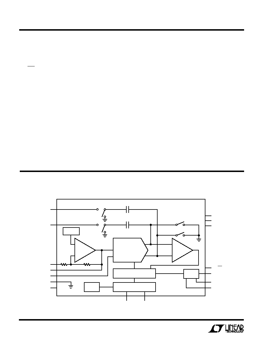
BLOCK DIAGRA
W
12-BIT CAPACITIVE DAC
COMP
REF AMP
+
2.048V REF
64k
GAIN
C
SAMPLE
C
SAMPLE
CONTROL LOGIC
SCK
CONV
16
15
INTERNAL
CLOCK
OUTPUT
DRIVER
ZEROING SWITCHES
AV
DD
1
12
DV
DD
14
8
10
11
9
V
SS
BIP/UNI
OV
DD
D
OUT
OGND
A
IN
+
3
4
7
5
6
2
13
A
IN
AGND1
AGND2
V
REF
DGND
1402 BD
+
SUCCESSIVE APPROXIMATION
REGISTER
64k
9
LTC1402
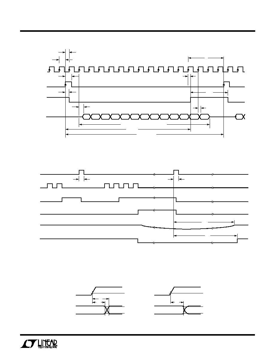
TI I G DIAGRA S
U
W
W
SCK
CONV
INTERNAL
S/H STATUS
D
OUT
t
7
t
3
1
2
3
4
5
6
7
8
9
10
11
12
13
14
15 16
1
2
t
2
t
6
t
8a
t
4
t
5
t
8
t
ACQ
SAMPLE
SAMPLE
HOLD
HOLD
Hi-Z
Hi-Z
t
CONV
REFRDY BIT + 12-BIT DATA WORD
D
OUT
REPRESENTS THE ANALOG INPUT FROM THE PREVIOUS CONVERSION
t
THROUGHPUT
1402 TD01
REF
D11
D9
D8
D7
D6
D5
D4
D3
D2
D1
D0
D10
REF
Nap Mode and Sleep Mode Waveforms
SCK
CONV
NAP
SLEEP
V
REF
t
1
t
12
t
11
t
1
REFRDY
NOTE: NAP AND SLEEP ARE INTERNAL SIGNALS. REFRDY APPEARS AS A BIT IN THE D
OUT
WORD.
1402 TD02
t
8
t
10
SCK
D
OUT
1402 TD03
V
IH
V
OH
V
OL
t
9
SCK
D
OUT
V
IH
90%
10%
SCK to D
OUT
Delay
10
LTC1402
APPLICATIO
N
S I
N
FOR
M
ATIO
N
W
U
U
U
DRIVING THE ANALOG INPUT
The differential analog inputs of the LTC1402 are easy to
drive. The inputs may be driven differentially or as a single-
ended input (i.e., the A
IN
input is grounded). The A
IN
+
and
A
IN
inputs are sampled at the same instant. Any unwanted
signal that is common to both inputs will be reduced by the
common mode rejection of the sample-and-hold circuit.
The inputs draw only one small current spike while charg-
ing the sample-and-hold capacitors at the end of conver-
sion. During conversion, the analog inputs draw only a
small leakage current. If the source impedance of the
driving circuit is low, then the LTC1402 inputs can be
driven directly. As source impedance increases, so will
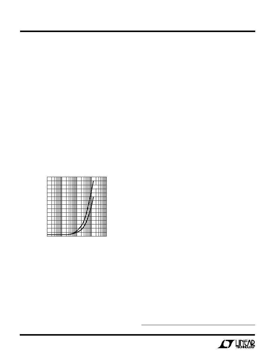
acquisition time (see Figure 1). For minimum acquisition
time with high source impedance, a buffer amplifier must
be used. The only requirement is that the amplifier driving
the analog input(s) must settle after the small current
spike before the next conversion starts (settling time must
be 50ns for full throughput rate).
Figure 1. Acquisition Time vs Source Resistance
in Bipolar and Unipolar Modes
SOURCE RESISTANCE (
)
300
ACQUISITION TIME (ns)
900
1100
1000
1300
1500
200
100
800
500
700
600
400
1200
1400
10
1k
10k
5V
100k
1402 F01
0
100
±
5V
second requirement is that the closed-loop bandwidth
must be greater than 40MHz to ensure adequate small-
signal settling for full throughput rate. If slower op amps
are used, more time for settling can be provided by
increasing the time between conversions. The best choice
for an op amp to drive the LTC1402 will depend on the
application. Generally, applications fall into two catego-
ries: AC applications where dynamic specifications are
most critical, and time domain applications where DC
accuracy and settling time are most critical. The following
list is a summary of the op amps that are suitable for
driving the LTC1402. More detailed information is avail-
able in the Linear Technology Databooks and on the
LinearView
TM
CD-ROM.
LT
®
1206: 60MHz Current Feedback Amplifier with Shut-
down Pin (Amplifier Draws 200
µ
A While in Shutdown).
±
5V to
±
15V supplies. Distortion is 80dB to 1MHz
(2V
P-P
into 30
). Good for AC applications. Dual avail-
able with shutdown as LT1207. Output swings to within
2V
BE
of the supply rails.
LT1223: 100MHz Video Current Feedback Amplifier. 6mA
supply current.
±
5V to
±
15V supplies. Low distortion at
frequencies above 400kHz. Low noise. Good for AC appli-
cations.
LT1227: 140MHz Video Current Feedback Amplifier. 10mA
supply current; has shutdown pin (draws 120
µ
A while in
shutdown).
±
5V to
±
15V supplies. Lowest distortion
( 92dB) at frequencies above 400kHz. Low noise. Best for
AC applications.
LT1229/LT1230: Dual and Quad 100MHz Current Feed-
back Amplifiers.
±
2V to
±
15V supplies. Low noise. Good
AC specifications, 6mA supply current each amplifier.
LT1360: 50MHz Voltage Feedback Amplifier. 3.8mA sup-
ply current.
±
5V to
±
15V supplies. Good AC and DC
specifications. 70ns settling to 0.5LSB.
LT1363: 70MHz, 1000V/
µ
s Op Amps. 6.3mA supply cur-
rent. Good AC and DC specifications. 60ns settling to
0.5LSB.
LT1364/LT1365: Dual and Quad 70MHz, 1000V/
µ
s Op
Amps. 6.3mA supply current per amplifier. 60ns settling
to 0.5LSB.
LinearView is a trademark of Linear Technology Corporation.
CHOOSING AN INPUT AMPLIFIER
Choosing an input amplifier is easy if a few requirements
are taken into consideration. First, to limit the magnitude
of the voltage spike seen by the amplifier from charging
the sampling capacitor, choose an amplifier that has a low
output impedance (< 100
) at the closed-loop bandwidth
frequency. For example, if an amplifier is used in a gain of
1 and has a unity-gain bandwidth of 50MHz, then the
output impedance at 50MHz must be less than 100
. The
11
LTC1402
APPLICATIO
N
S I
N
FOR
M
ATIO
N
W
U
U
U
LT1630: Dual 30MHz Rail-to-Rail Voltage FB Amplifier.
2.7V to
±
15V supplies. Very high A
VOL
, 500
µ
V offset and
520ns settling to 0.5LSB for a 4V swing. THD and noise
are 93dB to 40kHz and below 1LSB to 320kHz (A
V
= 1,
2V
P-P
into 1k
, V
S
= 5V), making the part excellent for AC
applications (to 1/3 Nyquist) where rail-to-rail perfor-
mance is desired. Quad version is available as LT1631.
LT1632: Dual 45MHz Rail-to-Rail Voltage FB Amplifier.
2.7V to
±
15V supplies. Very high A
VOL
, 1.5mV offset and
400ns settling to 0.5LSB for a 4V swing. It is suitable for
applications with a single 5V supply. THD and noise are
93dB to 40kHz and below 1LSB to 800kHz (A
V
= 1,
2V
P-P
into 1k
, V
S
= 5V), making the part excellent for AC
applications where rail-to-rail performance is desired.
Quad version is available as LT1633.
LT1813: Dual 100MHz 750V/
µ
s 3mA Voltage Feedback
Amplifier. 5V to
±
5V supplies. Distortion is 86dB to
100kHz and 77dB to 1MHz with
±
5V supplies (2V
P-P
into
500
). Excellent part for fast AC applications with
±
5V
supplies.
INPUT FILTERING AND SOURCE IMPEDANCE
The noise and the distortion of the input amplifier and
other circuitry must be considered since they will add to
the LTC1402 noise and distortion. The small-signal band-
width of the sample-and-hold circuit is 80MHz. Any noise
or distortion products that are present at the analog inputs
will be summed over this entire bandwidth. Noisy input
circuitry should be filtered prior to the analog inputs to
minimize noise. A simple 1-pole RC filter is sufficient for
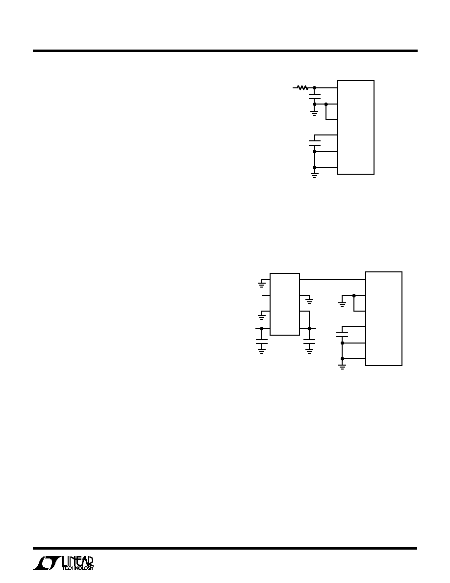
many applications. For example, Figure 2 shows a 68pF
capacitor from A
IN
+
to ground and a 51
source resistor
to limit the input bandwidth to 47MHz. The 68pF capacitor
also acts as a charge reservoir for the input sample-and-
hold and isolates the ADC input from sampling glitch-
sensitive circuitry.
High quality capacitors and resistors should be used since
these components can add distortion. NPO and silver mica
type dielectric capacitors have excellent linearity.
Carbon surface mount resistors can generate distortion
from self heating and from damage that may occur during
soldering. Metal film surface mount resistors are much
less susceptible to both problems. When high amplitude
unwanted signals are close in frequency to the desired signal
frequency, a multiple pole filter is required. Figure 3 shows
a simple implementation using an LTC1560-1 fifth order
elliptic continuous-time 1MHz filter.
LTC1402
A
IN
+
A
IN
V
REF
AGND1
AGND2
GAIN
1402 F02
3
4
2
6
5
7
10
µ
F
68pF
51
ANALOG
INPUT
Figure 2. RC Input Filter
LTC1560-1
1
2
3
4
8
7
6
5
0.1
µ
F
5V
0.1
µ
F
5V
V
IN
LTC1402
A
IN
+
A
IN
V
REF
AGND1
AGND2
GAIN
1402 F03
3
4
2
6
5
7
10
µ
F
Figure 3. 1MHz Fifth Order Elliptic Lowpass Filter
BIPOLAR AND UNIPOLAR INPUT RANGES
The
±
2V bipolar input range of the LTC1402 is optimized
for low noise and low distortion. Most op amps also
perform best over this same range, allowing direct cou-
pling to the analog inputs and eliminating the need for
special translation circuitry. The inputs of the LTC1402
may also be driven fully differential in bipolar mode with
a single supply. Each input should not swing more than
2V
P-P
individually to get the best performance from single
supply amplifiers.
The 0V to 4V range is ideal for single ended input use with
single supply applications.
12
LTC1402
APPLICATIO
N
S I
N
FOR
M
ATIO
N
W
U
U
U
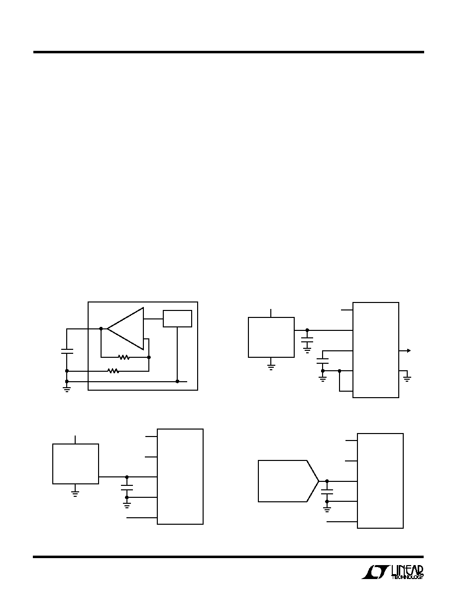
INTERNAL REFERENCE
The LTC1402 has an on-chip, temperature compensated,
curvature corrected, bandgap reference that is factory
trimmed to 2.048V. It is connected internally to a reference
amplifier, see Figure 4. The reference amplifier amplifies
the voltage at the V
REF
pin by 2 to create the required
internal reference voltage of 4.096V. This provides buffer-
ing for the high speed capacitive DAC. The reference
amplifier output V
REF
, (Pin 5) must be bypassed with a
capacitor to ground. The reference amplifier is stable with
capacitors of 1
µ
F or greater. For the best noise perfor-
mance, a 10
µ
F ceramic or a 10
µ
F tantalum in parallel with
a 0.1
µ
F ceramic is recommended.
The V
REF
pin can be driven with an external reference as
shown in Figure 5a. The GAIN pin (Pin 7) is tied to the
positive supply to disable the internal reference buffer.
A DAC may also be used to drive V
REF
as shown in
Figure 6. This is useful in applications where the peak
input signal amplitude may vary. The input span of the
Figure 5a. Using the LT1019-2.5 as an External Reference
LTC1402
LT1019-2.5
A
IN
+
ANALOG INPUT
5V
5V
A
IN
V
REF
V
OUT
V
IN
AGND2
GAIN
1402 F04a
3
4
5
6
7
10
µ
F
LTC1402
LT1019-2.5
A
IN
+
V
IN
2.5V
±
2.048V
5V
A
IN
V
REF
BIP
V
IN
AGND2
14
V
SS
GAIN
1402 F04a
3
4
5
6
7
10
µ
F
10
µ
F
Figure 5b. Bipolar Mode with Single Supply
Figure 4. LTC1402 Reference Circuit
64k
64k
REFERENCE
AMP
10
µ
F
GAIN
V
REF
BANGAP
REFERENCE
5
7
AGND2
6
4.096V
LTC1402
+
2.048V
1402 F04
Figure 6. Driving V
REF
with a DAC
LTC1402
A
IN
+
ANALOG INPUT
5V
A
IN
V
REF
AGND2
GAIN
1402 F06
3
4
5
6
7
10
µ
F
LTC1450
ADC can then be adjusted to match the peak input signal,
maximizing the signal-to-noise ratio. The filtering of the
internal LTC1402 reference amplifier will limit the band-
width and settling time of this circuit. A settling time of
5ms should be allowed after a reference adjustment.
DIFFERENTIAL INPUTS
The LTC1402 has a unique differential sample-and-hold
circuit that allows inputs from 2.5V to 5V. The ADC will
always convert the difference of A
IN
+
A
IN
independent
of the common mode voltage. The common mode rejec-
tion holds up at extremely high frequencies, see Figure 7.
The only requirement is that both inputs not exceed
2.5V or 5V. Integral nonlinearity errors (INL) and differ-
ential nonlinearity errors (DNL) are independent of the
common mode voltage. However, the bipolar zero error
(BZE) will vary. The change in BZE is typically less than
0.1% of the common mode voltage. Figure 5b shows the
use of bipolar mode with single 5V supply.
13
LTC1402
APPLICATIO
N
S I
N
FOR
M
ATIO
N
W
U
U
U
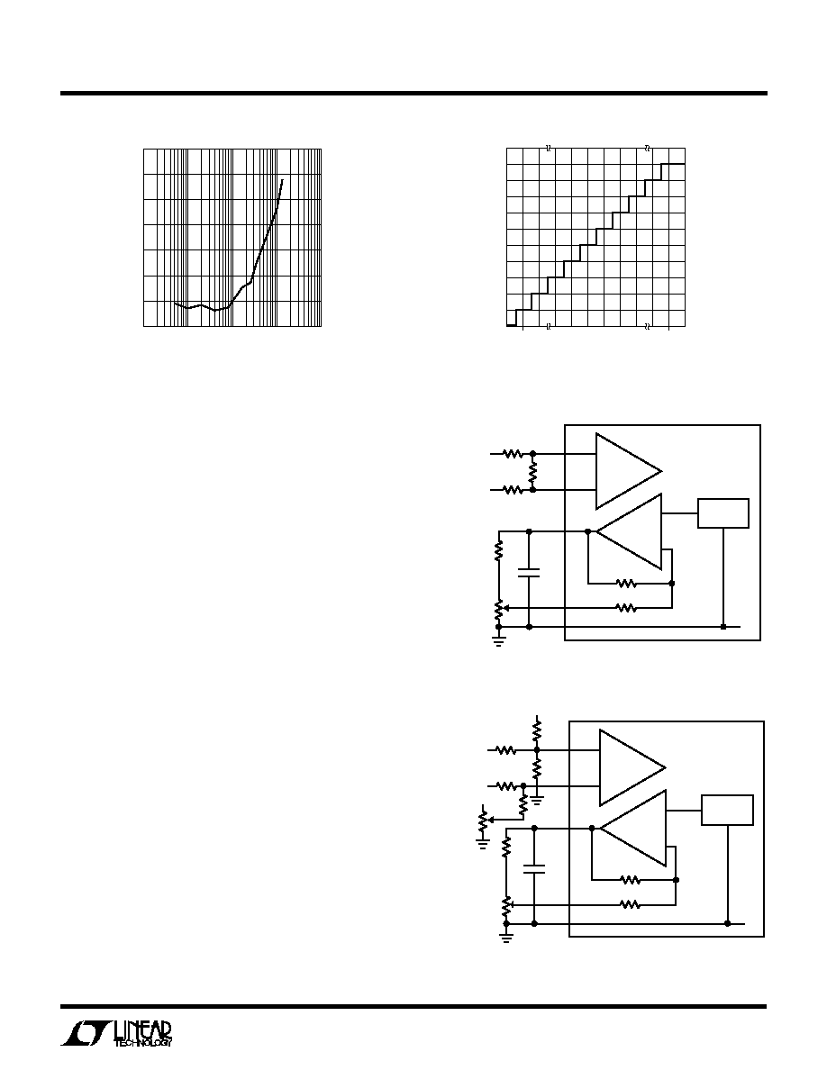
FULL-SCALE AND OFFSET ADJUSTMENT
Figure 8 shows the ideal input/output characteristics for
the LTC1402 in bipolar mode and unipolar mode. Figure 9a
shows the components required for full-scale error ad-
justment. Figure 9b includes the components for offset
and full-scale adjustment.
Adjustment in Bipolar Mode with Pin 8 Held High
The code transitions occur midway between successive
integer LSB values (i.e., FS + 0.5LSB, FS + 1.5LSB, FS
+ 2.5LSB,...FS 2.5LSB, FS 1.5LSB). The output at D
OUT
is two's complement binary with 1LSB = FS ( FS)/4096
= 4.096V/4096 = 1.0mV. In applications where absolute
accuracy is important, offset and full-scale errors can be
adjusted to zero. Offset error must be adjusted before full-
scale error. In Figure 9b, zero offset is achieved by adjust-
ing the offset applied to the A
IN
input. For zero offset
error, apply 0.5mV (i.e., 0.5LSB) to A
IN
+
and adjust the
offset at the A
IN
input using R8 until the output code
flickers between 0000 0000 0000 and 1111 1111 1111.
For full-scale adjustment in Figures 9a and 9b, apply an
input voltage of 2.0465V (FS 1.5LSB) to A
IN
+
and adjust
R5 until the output code flickers between 0111 1111 1110
and 0111 1111 1111.
Adjustment in Unipolar Mode with Pin 8 Held Low
The code transitions occur midway between successive
integer LSB values (i.e., FS + 0.5LSB, FS + 1.5LSB,
FS + 2.5LSB,...FS 2.5LSB, FS 1.5LSB). The output at
Figure 8. LTC1402 Transfer Characteristic
Figure 9a. Full-Scale Adjustment Circuit with
±
10LSB Range
Figure 7. CMRR vs Input Frequency
FREQUENCY (MHz)
40
AMPLITUDE (dB)
30
20
10
0
0.1
10
100
1000
1402 F07
50
60
70
1
INPUT VOLTAGE (V)
BIPOLAR OUTPUT CODE
UNIPOLAR OUTPUT CODE
1402 F08
011...111
011...110
011...101
100...000
100...001
100...010
111...111
111...110
111...101
000...000
000...001
000...010
FS 1LSB
(FS 1LSB)
64k
R1
51
R3
51
64k
REFERENCE
AMP
S/H
10
µ
F
R4
470k
R2
39k
R5
500
GAIN
V
REF
BANGAP
REFERENCE
5
ANALOG INPUT
0V TO 4.096V
OR
±
2.048V
7
A
IN
4
A
IN
+
3
AGND2
6
LTC1402
2.048V
1402 F09a
Figure 9b. Offset and Full-Scale Adjustment
Circuits with
±
10LSB Range
64k
R1
51
R3
51
64k
REFERENCE
AMP
S/H
10
µ
F
R4
470k
R2
24k
R7
7.5k
R5
500
GAIN
V
REF
BANGAP
REFERENCE
5
5V
5V
ANALOG INPUT
0V TO 4.096V
OR
±
2.048V
OFFSET
ADJ
FULL-SCALE
ADJ
7
A
IN
4
A
IN
+
3
AGND2
6
LTC1402
2.048V
1402 F09b
R8
10k
R6
24k

14
LTC1402
Low impedance analog and digital power supply common
returns are essential to low noise operation of the ADC and
the foil width for these tracks should be as wide as
possible. The traces connecting the pins and bypass
capacitors must be kept short and should be made as wide
as possible.
The LTC1402 has differential inputs to minimize noise
coupling. Common mode noise on the A
IN
+
and A
IN
leads
will be rejected by the input CMRR. The A
IN
input can be
used as a ground sense for the A
IN
+
input; the LTC1402 will
hold and convert the difference voltage between A
IN
+
and
A
IN
. The leads to A
IN
+
(Pin 3) and A
IN
(Pin 4) should be
kept as short as possible. In applications where this is not
possible, the A
IN
+
and A
IN
traces should be run side-by-
side to cancel noise coupling.
SUPPLY BYPASSING
High quality, low series resistance 10
µ
F ceramic bypass
capacitors should be used at the V
DD
and V
REF
pins.
Surface mount ceramic capacitors such as Murata
GRM235Y5V106Z016 provide excellent bypassing in a
small board space. Alternatively, 10
µ
F tantalum capaci-
tors in parallel with 0.1
µ
F ceramic capacitors can be used.
Bypass capacitors must be located as close to the pins as
possible. The traces connecting the pins and the bypass
capacitors must be kept short and should be made as wide
as possible.
POWER-DOWN MODES
Upon power-up, the LTC1402 is initialized to the active
state and is ready for conversion. The Nap and Sleep Mode
waveforms show the power-down modes for the LTC1402.
APPLICATIO
N
S I
N
FOR
M
ATIO
N
W
U
U
U
D
OUT
is binary with 1LSB = FS/4096 = 4.096V/4096 =
1.0mV. In applications where absolute accuracy is impor-
tant, offset and full-scale errors can be adjusted to zero.
Offset error must be adjusted before full-scale error. In
Figure 9b, zero offset is achieved by adjusting the offset
applied to the A
IN
input. For zero offset error apply
0.5mV (i.e., 0.5LSB) to A
IN
+
and adjust the offset at the
A
IN
input using R8 until the output code flickers between
0000 0000 0000 and 0000 0000 0001. For full-scale ad-
justment in Figures 9a and 9b, apply an input voltage of
2.0465V (FS 1.5LSBs) to A
IN
+
and adjust R5 until the
output code flickers between 1111 1111 1110 and 1111
1111 1111.
BOARD LAYOUT AND BYPASSING
Wire wrap boards are not recommended for high resolu-
tion and/or high speed A/D converters. To obtain the best
performance from the LTC1402, a printed circuit board
with ground plane is required. Layout for the printed
circuit board should ensure that digital and analog signal
lines are separated as much as possible. In particular, care
should be taken not to run any digital track alongside an
analog signal track.
An analog ground plane separate from the logic system
ground should be established under and around the ADC.
Pin 2 (AGND1), Pin 6 (AGND2), Pin 13 (DGND) and all
other analog grounds should be connected directly to an
analog ground plane. Pin 9 (OGND) should be connected
near Pin13 (DGND), where the analog ground plane ties to
the logic system ground. The V
REF
bypass capacitor and
the DV
DD
bypass capacitor should also be connected to
this analog ground plane, see Figure 10. No other digital
grounds should be connected to this analog ground plane.
Figure 10. Power Supply Grounding Practice
1402 F10
A
IN
+
AGND2
AGND1
V
REF
AV
DD
DV
DD
OV
DD
D
OUT
OGND
LTC1402
DIGITAL
SYSTEM
SYSTEM
GROUND
10
µ
F
10
µ
F
ANALOG
INPUT
CIRCUITRY
6
14
5
4
1
12
13
9
10
12
3V TO 5V
DGND
3
A
IN
V
SS
2
ANALOG GROUND PLANE
10
µ
F
+

15
LTC1402
APPLICATIO
N
S I
N
FOR
M
ATIO
N
W
U
U
U
Figure 11. Power Consumption vs Sample Rate
in Normal Mode, Nap Mode and Sleep Mode
CONV at Pin 16
The rising edge of CONV starts a conversion but subse-
quent rising edges at CONV, during the following 14 SCK
cycles of conversion, are ignored by the LTC1402. The
duty cycle of CONV can be arbitrarily chosen to be used as
a frame sync signal for the processor serial port. A simple
approach to generate CONV is to create a pulse that is one
SCK wide to drive the LTC1402 and then buffer this signal
with the appropriate number of inverters to drive the frame
sync input of the processor serial port. It is good practice
to drive the LTC1402 CONV input first to avoid digital noise
interference during the sample-to-hold transition triggered
by CONV at the start of conversion. Another point to con-
sider is the level of jitter in the CONV signal if the input
signals have fast transients or sinewaves. Some proces-
sors can be programmed to generate a convenient frame
sync pulse at their serial port, but often this signal is de-
rived from a jittery processor phase locked loop clock
multiplier. This is true even if a low jitter crystal clock is the
reference for the processor clock multiplier.
SCK at Pin 15
The rising edge of SCK advances the conversion process
and also udpates each bit in the D
OUT
data stream. After
CONV rises, the second rising edge of SCK sends out the
REFREADY bit. Subsequent edges send out the 12 data
bits, with the MSB sent first. A simple approach is to
generate SCK to drive the LTC1402 and then buffer this
signal with the appropriate number of inverters to drive the
serial clock input of the processor serial port. The rising
edge of SCK is guaranteed to coincide with stable data at
D
OUT
. It is good practice to drive the LTC1402 SCK input
first to avoid digital noise interference during the internal
bit comparison decision by the internal high speed com-
parator. Unlike the CONV input, the SCK input is not
sensitive to jitter because the input signal is already
sampled and held constant.
D
OUT
at Pin 10
Upon power-up, the D
OUT
output is automatically reset to
the high impedance state. The D
OUT
output remains in high
impedance until a new conversion is started. D
OUT
sends
out 13 bits in the output data stream after the second rising
edge of SCK after the start of conversion with the rising
The SCK and CONV inputs control the power-down modes
(see Timing Diagrams). Two rising edges at CONV, with-
out any intervening rising edges at SCK, put the LTC1402
in Nap mode and the power drain drops from 90mW to
15mW. The internal reference remains powered in Nap
mode. One or more rising edges at SCK wake up the
LTC1402 for service very quickly, and CONV can start an
accurate conversion within a clock cycle. Four rising edges
at CONV, without any intervening rising edges at SCK, put
the LTC1402 in Sleep mode and the power drain drops
from 90mW to 10
µ
W. One or more rising edges at SCK
wake up the LTC1402 for operation. The internal reference
(V
REF
) takes 2ms to slew and settle with a 10
µ
F load, and
the REFREADY bit in the D
OUT
stream takes an additional
10ms to go high after the reference output Pin 5 (V
REF
) has
finished slewing. Figure 11 shows the power consumption
versus the conversion rate. Note that, for slower conver-
sion rates, the Nap and Sleep modes can be used for sub-
stantial reductions in power consumption.
SAMPLE RATE (MHz)
0.01
0.1
SUPPLY CURRENT (mA)
10
1
0.01
0.1
1
1402 F11
0.001
100
10
V
DD
CURRENT
DUAL
±
5V
V
SS
CURRENT
DUAL
±
5V
V
DD
CURRENT
SINGLE 5V
V
SS
CURRENT
SINGLE 5V
V
DD
CURRENT
SLEEP MODE
V
DD
CURRENT
NAP MODE
DIGITAL INTERFACE
The LTC1402 has a 3-wire SPI (Serial Protocol Interface)
interface. The SCK and CONV inputs and D
OUT
output
implement this interface. The SCK and CONV inputs are TTL
compatible and also accept swings from 3V or 5V logic. The
amplitude of D
OUT
can easily produce 5V logic or 3V logic
swings by tying the independent output supply Pin 11
(OV
DD
) to the same supply as system logic. A detailed
description of the three serial port signals follows.
16
LTC1402
edge of CONV. Please note the delay specification from
SCK to a valid D
OUT
. D
OUT
is always guaranteed to be valid
by the next rising edge of SCK.
DIGITAL JITTER AT CONV (PIN 16)
In high speed applications, where high amplitude sinewaves
above 100kHz are sampled, the CONV signal must have as
little jitter as possible (10ps or less). The square wave
output of a common crystal clock module usually meets
this requirement easily. The challenge is to generate a CONV
signal from this crystal clock without jitter corruption from
other digital circuits in the system. A clock divider and any
gates in the signal path from the crystal clock to the CONV
input should not share the same integrated circuit with
other parts of the system. As shown in the interface circuit
examples, the LTC1402's SCK and CONV inputs should be
driven first with digital buffers used to drive the serial port
interface. Also note that the master clock in the DSP may
already be corrupted with jitter, even if it comes directly
from the DSP crystal. Another problem with high speed
processor clocks is that they often use a low cost, low
speed crystal (i.e., 10MHz) to generated a fast, but jittery,
phase locked loop system clock (i.e., 40MHz). The jitter, in
these PLL-generated high speed clocks, can be several
nanoseconds. Note that if you choose to use the frame
sync signal generated by the DSP port, this signal will have
the same jitter of the DSP's master clock.
SERIAL TO PARALLEL CONVERSION
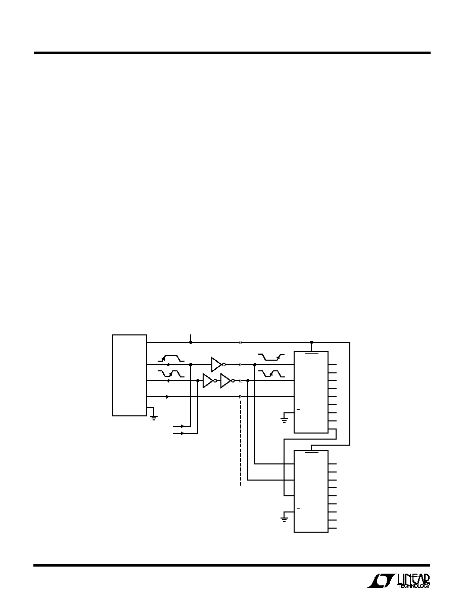
You can take advantage of the serial interface of the LTC1402
in a parallel data system to minimize bus wiring conges-
tion in the PC board layout. Figure 12 shows an example
of this interface. It is best to send the SCK and CONV
signals to the LTC1402, and then bus them together across
the board to avoid excessive time skew among the three
signals. It is usually not necessary to buffer D
OUT
, if the PC
track is not too long. Buffering SCK and CONV prevents
jitter from corrupting these signals. The relative phase
between SCK and CONV affects the position of the parallel
word at the output of the 74HC595. The position of the
output word in Figure 12 assumes 16 clocks between each
CONV rising edge, and the CONV pulse is one clock wide.
APPLICATIO
N
S I
N
FOR
M
ATIO
N
W
U
U
U
Figure 12. Serial to Parallel Interface
SRCLR
QA
QB
QC
QD
QE
QF
QG
RCK
SRCK
SER
G
QH
QH
15
1
2
3
4
5
6
12
10
10
11
14
13
7
9
SRCLR
QA
QB
QC
QD
QE
QF
QG
RCK
74ACT04
SRCK
SER
74HC595
74HC595
G
11
5V
16
15
10
9
3-WIRE SERIAL
INTERFACE LINK
QH
QH
15
1
2
3
4
5
6
12
11
14
13
1402 F12
7
D0
D1
D2
D3
D4
D5
D7
D8
D9
D10
D11
REFRDY
D6
9
OV
DD
CONV
SCK
LTC1402
D
OUT
OGND
CONV
CLK
17
LTC1402
APPLICATIO
N
S I
N
FOR
M
ATIO
N
W
U
U
U
Figure 13. DSP Serial Interface to TMS320C54x
1402 F13
11
16
15
10
9
3-WIRE SERIAL
INTERFACE LINK
OV
DD
CONV
SCK
LTC1402
D
OUT
V
CC
BFSR
BCLKR
TMS320C54x
BDR
OGND
CONV
CLK
5V
REF
B11
B10
HARDWARE INTERFACE TO TMS320C54x
The LTC1402 is a serial output ADC whose interface has
been designed for high speed buffered serial ports in fast
digital signal processors (DSPs). Figure 13 shows an
example of this interface using a TMS320C54X.
The buffered serial port in the TMS320C54x has direct
access to a 2kB segment of memory. The ADC's serial data
can be collected in two alternating 1kB segments, in real
time, at the full 2.2Msps conversion rate of the LTC1402.
The DSP assembly code sets frame sync mode at the BFSR
pin to accept an external positive going pulse, and the
serial clock at the BCLKR pin to accept an external positive
edge clock. Buffers near the LTC1402 may be added to
drive long tracks to the DSP to prevent corruption of the
signal to LTC1402. This configuration is adequate to
traverse a typical system board, but source resistors at the
buffer outputs, and termination resistors at the DSP may
be needed to match the characteristic impedance of very
long transmission lines. If you need to terminate the D
OUT
transmission line, buffer it first with one or two 74ACxx
gates. The TTL threshold inputs of the DSP port respond
properly to the 2.5V swing of the terminated transmission
lines. The OV
DD
supply output driver supply voltage can be
driven directly from the DSP.
; ***************************************************************************
; Files: BSP2KB.ASM ->
; 2kbyte collection into DSKPlus TMS320C542 with Serial Port interface to LTC1402
; first element at 1024, last element at 1023, two middle elements at 2047 and 0000
; bipolar mode
; ***************************************************************************
.width
160
.length
110
.title "sineb0 BSP in auto buffer mode"
.mmregs
.setsect ".text",
0x500,0
;Set address of executable
.setsect "vectors", 0x180,0
;Set address of incoming 1402 data
.setsect "buffer", 0x800,0
;Set address of BSP buffer for clearing
.setsect "result",
0x1800,0
;Set address of result for clearing
.text
;.text marks start of code
start: ;Make sure /PWRDWN is low at J1-9 to turn off AC01 adc
tim=#0fh
prd=#0fh
tcr = #10h
; stop timer
tspc = #0h
; stop TDM serial port to AC01
pmst = #01a0h ; set up iptr. Processor Mode STatus register
sp = #0700h
; init stack pointer.
dp = #0
; data page
ar2 = #1800h
; pointer to computed receive buffer.
ar3 = #0800h
; pointer to Buffered Serial Port receive buffer
ar4 = #0h
; reset record counter
call sineinit
; Double clutch the initialization to insure a proper
sinepeek:
; insert debugger break here to view results
call sineinit
; reset. The external frame sync must occur 2.5 clocks
; or more after the port comes out of reset.
wait goto wait

18
LTC1402
APPLICATIO
N
S I
N
FOR
M
ATIO
N
W
U
U
U
; ----------------Buffered Receive Interrupt Routine ------------------
breceive:
ifr = #10h
; clear interrupt flags
TC = bitf(@BSPCE,#4000h)
; check which half (bspce(bit14)) of buffer
if (NTC) goto bufull
; if this still the first half get next half
bspce = #(2023h + 08000h)
; turn on halt for second half (bspce(bit15))
return_enable
; --------------mask and shift input data after 2k buffer is full-----
bufull:
b = *ar3+ << -2
; load acc b with BSP buffer and shift right 2
b = #00FFFh & b
; mask out the REF bit and the 3 other tristate bits
b = #00800h ^ b
; invert BIPOLAR MSB. Comment this line in UNIPOLAR mode
*ar2+ = data(#0bh)
; store B to out buffer and advance AR2 pointer
TC = (@ar2 == #02000h) ; output buffer is 2k starting at 1800h
if (TC) goto start
; restart if out buffer is at 1fffh
goto bufull
; ------------------dummy bsend return------------------------
bsend return_enable
;this is a dummy return to define bsend
;in vector table below
; ---------------------- end ISR ----------------------------
;initialize buffered serial port
**********************************************************************
* BSP initialization code for the `C54x DSKplus
*
* for use with 1402 in standard mode
*
* BSPC and SPC are the same in the `C542
*
**********************************************************************
ON
.set 1
OFF
.set !ON
YES
.set 1
NO
.set !YES
BIT_8
.set 2
BIT_10
.set 1
BIT_12
.set 3
BIT_16
.set 0
GO
.set 0x80
**********************************************************************
* This is an example of how to initialize the Buffered Serial Port (BSP).
* The BSP is initialized to require an external CLK and FSX for
* operation. The data format is 16-bits, burst mode, with autobuffering
* enabled.
*
*
*****************************************************************************************************
*Timing at BSP pins in DSKPLUS TMS320c542 board with inverters at BCLKR and BFSR.
*
*BFSR Pin JP1-20 ~\___/~~~~~~~~~~~~~~~~~~~~~~~~~~~~~~~~~~~~~~~~~~~~~~~~~~~~~~~~~~~\___/~~~~~~~~~~*
*BCLKR Pin JP1-14 _/~\_/~\_/~\_/~\_/~\_/~\_/~\_/~\_/~\_/~\_/~\_/~\_/~\_/~\_/~\_/~\_/~\_/~\_/~\_/~\_/
*
*BDR Pin JP1-26 -_--_--<REF-B11-B10-B09-B08-B07-B06-B05-B04-B03-B02-B01-B00>--_--_--<REF-B11-
*
*CLKIN Pin JP5-09 ~~~~~\_______/~~~~~~~\_______/~~~~~~~\_______/~~~~~~~\_______/~~~~~~~\_______/~~~~ *
*
*
*A 2 place right shift is needed to right justify the input data.
*
*The REF bit is also be masked in this example
*
*****************************************************************************************************
*
Loopback
.set NO
;(digital looback mode?)
DLB bit
Format
.set BIT_16
;(Data format? 16,12,10,8)
FO bit
IntSync
.set NO
;(internal Frame syncs generated?)
TXM bit
IntCLK
.set NO
;(internal clks generated?)
MCM bit
BurstMode
.set YES
;(if BurstMode=NO, then Continuous)
FSM bit
CLKDIV
.set 3
;(3=default value, 1/4 CLOCKOUT)
PCM_Mode .set NO
;(Turn on PCM mode?)
FS_polarity
.set NO
;(change polarity)YES=^^^\_/^^^, NO=___/^\___
CLK_polarity .set YES
;(change polarity)for BCLKR YES=_/^, NO=~\_
Frame_ignore .set !YES
;(inverted !YES -ignores frame)
XMTautobuf .set NO
;(transmit autobuffering)
RCVautobuf
.set YES
;(receive autobuffering)
XMThalt
.set NO
;(transmit buff halt if XMT buff is full)
RCVhalt
.set NO
;(receive buff halt if RCV buff is full)
XMTbufAddr .set 0x800
;(address of transmit buffer)
XMTbufSize
.set 0x000
;(length of transmit buffer)

19
LTC1402
RCVbufAddr
.set 0x800
;(address of receive buffer)
RCVbufSize
.set 0x800
;(length of receive buffer)works up to 800
*
*
*
**********************************************************************
.eval ((Loopback >> 1)|((Format & 2)<<1)|(BurstMode <<3)|(IntCLK <<4)|(IntSync <<5)) ,SPCval
.eval ((CLKDIV)|(FS_polarity <<5)|(CLK_polarity<<6)|((Format & 1)<<7)|(Frame_ignore<<8)|(PCM_Mode<<9)), SPCEval
.eval (SPCEval|(XMTautobuf<<10)|(XMThalt<<12)|(RCVautobuf<<13)|(RCVhalt<<15)), SPCEval
sineinit:
bspc = #SPCval
; places buffered serial port in reset
ifr = #10h
; clear interrupt flags
imr = #210h
; Enable HPINT,enable BRINT0
intm = 0
; all unmasked interrupts are enabled.
bspce = #SPCEval
; programs BSPCE and ABU
axr = #XMTbufAddr
; initializes transmit buffer start address
bkx = #XMTbufSize
; initializes transmit buffer size
arr = #RCVbufAddr
; initializes receive buffer start address
bkr = #RCVbufSize
; initializes receive buffer size
bspc = #(SPCval | GO)
; bring buffered serial port out of reset
return
;for transmit and receive because GO=0xC0
.space 16*32
;clear a chunk at the end to mark the end
;======================================================================
;
; VECTORS
;
;======================================================================
.sect "vectors"
;The vectors start here
;get BSP vectors
; ***************************************************************************
;
Vector Table for the `C54x DSKplus
;
BSP vectors and Debugger vectors
;
TDM vectors just return
; ***************************************************************************
; The vectors in this table can be configured for processing external and
; internal software interrupts. The DSKplus debugger uses four interrupt
; vectors. These are RESET, TRAP2, INT2, and HPIINT.
; * DO NOT MODIFY THESE FOUR VECTORS IF YOU PLAN TO USE THE DEBUGGER *
;
; All other vector locations are free to use. When programming always be sure
; the HPIINT bit is unmasked (IMR=200h) to allow the communications kernel and
; host PC interact. INT2 should normally be masked (IMR(bit 2) = 0) so that the
; DSP will not interrupt itself during a HINT. HINT is tied to INT2 externally.
;
;
;
.mmregs
reset goto #80h
;00; RESET * DO NOT MODIFY IF USING DEBUGGER *
nop
nop
nmi return_enable
;04; non-maskable external interrupt
nop
nop
nop
trap2 goto #88h
;08; trap2 * DO NOT MODIFY IF USING DEBUGGER *
nop
nop
.space 52*16
;0C-3F: vectors for software interrupts 18-30
int0
return_enable
;40; external interrupt int0
nop
nop
nop
int1 return_enable
;44; external interrupt int1
nop
nop
nop
int2 return_enable
;48; external interrupt int2
nop
nop
nop
APPLICATIO
N
S I
N
FOR
M
ATIO
N
W
U
U
U

20
LTC1402
tint
return_enable
;4C; internal timer interrupt
nop
nop
nop
brint goto breceive
;50; BSP receive interrupt
nop
nop
nop
bxint goto bsend
;54; BSP transmit interrupt
nop
nop
nop
trint
return_enable
;58; TDM receive interrupt
nop
nop
nop
APPLICATIO
N
S I
N
FOR
M
ATIO
N
W
U
U
U
RELATED PARTS
1402i LT/TP 1099 · PRINTED IN USA
©
LINEAR TECHNOLOGY CORPORATION 1999
Linear Technology Corporation
1630 McCarthy Blvd., Milpitas, CA 95035-7417
(408) 432-1900
q
FAX: (408) 434-0507
q
www.linear-tech.com
PART NUMBER
RESOLUTION
SPEED
COMMENTS
16-Bit
LTC1604
16
333ksps
±
2.5V Input Range,
±
5V Supply
LTC1605
16
100ksps
±
10V Input Range, Single 5V Supply
14-Bit
LTC1414
14
2.2Msps
175mW, 80dB SINAD and 95dB SFDR
LTC1419
14
800ksps
150mW, 81.5dB SINAD and 95dB SFDR
LTC1416
14
400ksps
75mW, Low Power with Excellent AC Specs
LTC1418
14
200ksps
15mW, Single 5V, Serial/Parallel I/O
12-Bit
LTC1412
12
3Msps
150mW, 72dB SINAD and 82dB SFDR
LTC1410
12
1.25Msps
150mW, 71.5dB SINAD and 84dB THD
LTC1415
12
1.25Msps
55mW, Single 5V Supply
LTC1409
12
800ksps
80mW, 71.5dB SINAD and 84dB THD
LTC1404
12
600ksps
High Speed Serial I/O in SO-8 Package
LTC1400
12
400ksps
High Speed Serial I/O in SO-8 Package
txint return_enable
;5C; TDM transmit interrupt
nop
nop
int3 return_enable
;60; external interrupt int3
nop
nop
nop
hpiint dgoto #0e4h
;64; HPIint * DO NOT MODIFY IF USING
DEBUGGER *
nop
nop
.space 24*16
;68-7F; reserved area
.sect "buffer"
;Set address of BSP buffer for clearing
.space 16*0x800
.sect "result"
;Set address of result for clearing
.space 16*0x800
.end
PACKAGE DESCRIPTIO
N
U
Dimensions in inches (millimeters) unless otherwise noted.
GN Package
16-Lead Plastic SSOP (Narrow 0.150)
(LTC DWG # 05-08-1641)
GN16 (SSOP) 1098
* DIMENSION DOES NOT INCLUDE MOLD FLASH. MOLD FLASH
SHALL NOT EXCEED 0.006" (0.152mm) PER SIDE
** DIMENSION DOES NOT INCLUDE INTERLEAD FLASH. INTERLEAD
FLASH SHALL NOT EXCEED 0.010" (0.254mm) PER SIDE
0.016 0.050
(0.406 1.270)
0.015
±
0.004
(0.38
±
0.10)
×
45
°
0
°
8
°
TYP
0.007 0.0098
(0.178 0.249)
0.053 0.068
(1.351 1.727)
0.008 0.012
(0.203 0.305)
0.004 0.0098
(0.102 0.249)
0.0250
(0.635)
BSC
1
2
3
4
5
6
7
8
0.229 0.244
(5.817 6.198)
0.150 0.157**
(3.810 3.988)
16 15 14 13
0.189 0.196*
(4.801 4.978)
12 11 10 9
0.009
(0.229)
REF