Äîêóìåíòàöèÿ è îïèñàíèÿ www.docs.chipfind.ru
1
LTC1264-7
Linear Phase, Group Delay
Equalized, 8th Order
Lowpass Filter
S
FEATURE
s
Steeper Roll-Off Than Bessel Filters
s
High Speed: f
C
200kHz
s
Phase Equalized Filter in a 14-Pin Package
s
Phase and Group Delay Response Fully Tested
s
Transient Response Exhibits 5% Overshoot and
No Ringing
s
65dB THD or Better Throughout a 100kHz Passband
s
No External Components Needed
D
U
ESCRIPTIO
The LTC1264-7 is a clock-tunable monolithic 8th order
lowpass filter with linear passband phase and flat group
delay. The amplitude response approximates a maximally
flat passband and exhibits steeper roll-off than an equiva-
lent 8th order Bessel filter. For instance, at twice the cutoff
frequency the filter attains 28dB attenuation (vs 12dB for
Bessel), while at three times the cutoff frequency the filter
attains 55dB attenuation (vs 30dB for Bessel). The cutoff
frequency of the LTC1264-7 is tuned via an external TTL or
CMOS clock.
The clock-to-cutoff frequency ratio of the LTC1264-7 can
be set to 25:1 (pin 10 to V
+
) or 50:1 (pin 10 to V
).
When the filter operates at clock-to-cutoff frequency ratio
of 25:1, the input is double-sampled to lower the risk of
aliasing.
The LTC1264-7 is optimized for speed. Depending on the
operating conditions, cutoff frequencies between 200kHz
and 250kHz can be obtained. (Please refer to the Passband
vs Clock Frequency graphs.)
The LTC1264-7 is pin-compatible with the LTC1064-X
series.
U
S
A
O
PPLICATI
s
Data Communication Filters
s
Time Delay Networks
s
Phase Matched Filters
U
A
O
PPLICATI
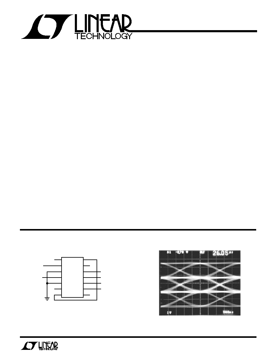
TYPICAL
200kHz Linear Phase Lowpass Filter
1
2
3
4
5
6
7
14
13
12
11
10
9
8
LTC1264-7
V
IN
8V
8V
f
CLK
= 5MHz
8V
V
OUT
NOTE: THE POWER SUPPLIES SHOULD BE BYPASSED BY A
0.1
µ
F CAPACITOR CLOSE TO THE PACKAGE AND ANY PRINTED
CIRCUIT BOARD ASSEMBLY SHOULD MAINTAIN A DISTANCE
OF AT LEAST 0.2 INCHES BETWEEN ANY OUTPUT OR INPUT
PIN AND THE f
CLK
LINE.
1264-7 TA01
4-Level PAM Eye Diagram
1264-7 TA02
500ns/DIV
1V/DIV
f
CLK
= 5MHz
f
C
= 200kHz
2
LTC1264-7
A
U
G
W
A
W
U
W
A
R
BSOLUTE
XI
TI
S
Total Supply Voltage (V
+
to V
) .......................... 16.5V
Power Dissipation ............................................. 400mW
Burn-In Voltage ................................................... 16.5V
Voltage at Any Input ..... (V
0.3V)
V
IN
(V
+
+ 0.3V)
Storage Temperature Range ............... 65
°
C to 150
°
C
Operating Temperature Range
LTC1264-7C ...................................... 40
°
C to 85
°
C
LTC1264-7M ................................... 55
°
C to 125
°
C
Lead Temperature (Soldering, 10 sec) ................. 300
°
C
(Note 1)
ELECTRICAL C
C
HARA TERISTICS
V
S
=
±
7.5V, R
L
= 10k, T
A
= 25
°
C, f
CUTOFF
= 100kHz or 50kHz, f
CLK
= 2.5MHz, TTL or CMOS level (maximum clock rise or fall
time
1
µ
s) and all gain measurements are referenced to passband gain, unless otherwise specified.
PARAMETER
CONDITIONS
MIN
TYP
MAX
UNITS
Passband Gain
0.1Hz
f
0.25 f
CUTOFF
f
TEST
= 25kHz, (f
CLK
/ f
C
) = 25:1
q
0.50
0.10
0.50
dB
Gain at 0.50 f
CUTOFF
(Note 3)
f
TEST
= 50kHz, (f
CLK
/ f
C
) = 25:1
q
0.50
0.20
dB
f
TEST
= 25kHz, (f
CLK
/ f
C
) = 50:1
q
0.65
0.15
0.30
dB
Gain at 0.75 f
CUTOFF
f
TEST
= 75kHz, (f
CLK
/ f
C
) = 25:1
q
1.5
1.0
0.1
dB
Gain at f
CUTOFF
f
TEST
= 100kHz, (f
CLK
/ f
C
) = 25:1
q
3.7
3.0
1.9
dB
f
TEST
= 50kHz, (f
CLK
/ f
C
) = 50:1
q
4.5
3.0
2.3
dB
Gain at 2.0 f
CUTOFF
f
TEST
= 200kHz, (f
CLK
/ f
C
) = 25:1
q
34
28
20
dB
f
TEST
= 100kHz, (f
CLK
/ f
C
) = 50:1
q
34
30
27
dB
Gain with f
CLK
= 20kHz
f
TEST
= 200Hz, (f
CLK
/ f
C
) = 50:1
0.7
0.3
0.1
dB
Gain with f
CLK
= 400kHz, V
S
=
±
2.375V
f
TEST
= 8kHz, (f
CLK
/ f
C
) = 25:1
0.2
0.15
0.5
dB
f
TEST
= 16kHz, (f
CLK
/ f
C
) = 25:1
3.5
2.70
1.4
dB
Gain with f
CLK
= 4MHz
f
TEST
= 160kHz, V
IN
= 1V
RMS
(f
CLK
/ f
C
) = 25:1, T
A
= 0
°
C to 70
°
C
0.00
±
1.0
dB
(f
CLK
/ f
C
) = 25:1
q
3.0
dB
Phase Factor (
F )
(f
CLK
/ f
C
) = 25:1, f
f
CUTOFF
407
±
2
Deg
Phase = 180
°
F (f/f
C
)
(f
CLK
/ f
C
) = 50:1, f
f
CUTOFF
388
±
2
Deg
(Note 1)
(f
CLK
/ f
C
) = 25:1, f
f
CUTOFF
q
392
423
Deg
(f
CLK
/ f
C
) = 50:1, f
f
CUTOFF
q
374
414
Deg
Phase Nonlinearity
(f
CLK
/ f
C
) = 25:1, f
f
CUTOFF
±
1.0
%
(Note 1)
(f
CLK
/ f
C
) = 50:1, f
f
CUTOFF
±
1.0
%
(f
CLK
/ f
C
) = 25:1, f
f
CUTOFF
q
±
2.0
%
(f
CLK
/ f
C
) = 50:1, f
f
CUTOFF
q
±
2.0
%
W
U
U
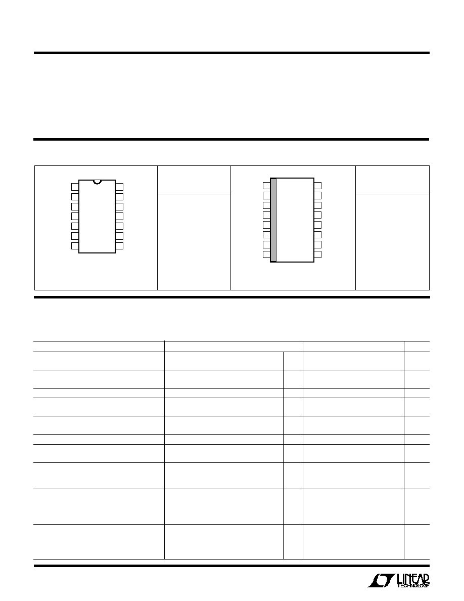
PACKAGE/ORDER I FOR ATIO
ORDER PART
NUMBER
LTC1264-7CN
LTC1264-7CJ
LTC1264-7MJ
ORDER PART
NUMBER
LTC1264-7CS
1
2
3
4
5
6
7
TOP VIEW
J PACKAGE
14-LEAD CERAMIC DIP
14
13
12
11
10
9
8
NC
V
IN
GND
V
+
NC
LP (A)
R
IN
(A)
OUT (C)
NC
V
f
CLK
25/50
V
OUT
NC
N PACKAGE
14-LEAD PLASTIC DIP
TOP VIEW
S PACKAGE
16-LEAD PLASTIC SOL
1
2
3
4
5
6
7
8
16
15
14
13
12
11
10
9
NC
V
IN
GND
V
+
NC
NC
LP (A)
R
IN
(A)
OUT (C)
NC
V
NC
f
CLK
25/50
NC
V
OUT
T
JMAX
= 150
°
C,
JA
= 65
°
C/W (J )
T
JMAX
= 110
°
C,
JA
= 65
°
C/W (N )
T
JMAX
= 110
°
C,
JA
= 85
°
C/W
3
LTC1264-7
ELECTRICAL C
C
HARA TERISTICS
PARAMETER
CONDITIONS
MIN
TYP
MAX
UNITS
Group Delay (t
d
)
(f
CLK
/ f
C
) = 25:1, f
f
CUTOFF
11.3
µ
s
t
d
= (
F/ 360)(1/f
C
);
(f
CLK
/ f
C
) = 50:1, f
f
CUTOFF
21.6
µ
s
(Note 2, 3)
(f
CLK
/ f
C
) = 25:1, f
f
CUTOFF
q
10.9
11.7
µ
s
(f
CLK
/ f
C
) = 50:1, f
f
CUTOFF
q
20.8
22.9
µ
s
Group Delay Ripple
(f
CLK
/ f
C
) = 25:1, f
f
CUTOFF
±
1.0
%
(Note 2)
(f
CLK
/ f
C
) = 50:1, f
f
CUTOFF
±
1.0
%
(f
CLK
/ f
C
) = 25:1, f
f
CUTOFF
q
±
2.0
%
(f
CLK
/ f
C
) = 50:1, f
f
CUTOFF
q
±
2.0
%
Input Frequency Range
(f
CLK
/ f
C
) = 25:1
<f
CLK
kHz
(Table 9, 10)
(f
CLK
/ f
C
) = 50:1
<f
CLK
/2
kHz
Maximum f
CLK
V
S
= Single 5V (GND = 2V)
2
MHz
V
S
=
±
5V
3
MHz
V
S
=
±
7.5V
5
MHz
Clock Feedthrough
25:1,
±
7.5V, f = f
CLK
120
µ
V
RMS
Wideband Noise
V
S
= Single 5V
140
±
5%
µ
V
RMS
(1Hz
f < f
CLK
)
V
S
=
±
5V
160
±
5%
µ
V
RMS
V
S
=
±
7.5V
175
±
5%
µ
V
RMS
Input Impedance
30
50
75
k
Output DC Voltage Swing
V
S
=
±
2.375V
±
1.0
V
(Note 4)
V
S
=
±
5V
q
±
2.0
±
2.3
V
V
S
=
±
7.5V
q
±
3.0
±
3.8
V
Output DC Offset
25:1, V
S
=
±
5V
±
100
±
220
mV
(f
CLK
= 1MHz)
50:1, V
S
=
±
5V
±
100
±
220
mV
Output DC Offset TempCo
25:1, V
S
=
±
5V
±
200
µ
V/
°
C
50:1, V
S
=
±
5V
±
200
µ
V/
°
C
Power Supply Current
V
S
=
±
2.375V
11
22
mA
(f
CLK
= 1MHz)
q
22
mA
V
S
=
±
5V
14
23
mA
q
26
mA
V
S
=
±
7.5V
17
28
mA
q
32
mA
Power Supply Range
±
2.375
±
8
V
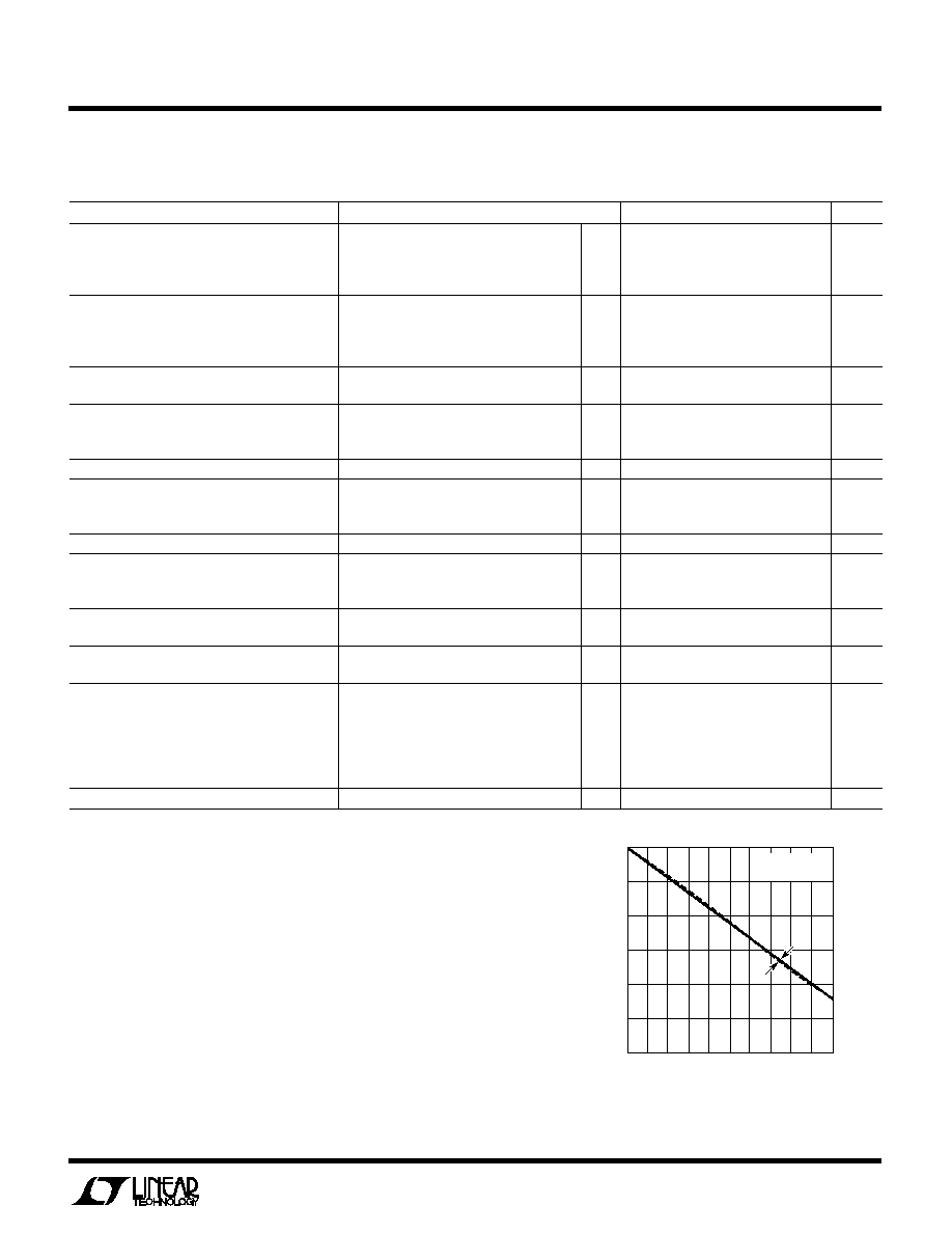
The
q
denotes specifications which apply over the full operating temperature range.
Note 1: Input frequencies, f, are linearly phase shifted through the filter as long as f
f
C
;
f
C
= cutoff frequency.
Figure 1 curve (A) shows the typical phase response of an LTC1264-7 operating at
f
CLK
= 2.5MHz, f
C
= 100kHz. An endpoint straight line, curve (B), depicts the ideal linear
phase response of the filter. It is described by: phase shift = 180
°
F (f/f
C
); f
f
C
.
F is arbitrarily called the "phase factor" expressed in degrees. The phase factor together
with the specified deviation from the ideal straight line allows the calculation of the phase
at a given frequency. Note, the maximum phase nonlinearity, Figure 1, occurs at the vicinity
of f = 0.25 f
C
and = 0.75 f
C
. Example: The phase shift at 70kHz of the LTC1264-7 shown in
Figure 1 is: phase shift = 180
°
407
°
(70kHz/100kHz)
±
nonlinearity
=
104.9
°
±
1% or 104.9
° ±
1.05
°
.
Note 2: Group delay and group delay deviation are calculated from the measured phase
factor and phase deviation specifications.
Note 3: The filter cutoff frequency is abbreviated as f
CUTOFF
or f
C
.
Note 4: The AC swing is typically 9V
P-P
, 5.6V
P-P
, 1.8V
P-P
with
±
7.5V,
±
5V,
±
2.5V supply
respectively. For more information refer to the THD + Noise vs Input graphs.
Figure 1. Phase Response in the Passband (Note 1)
V
S
=
±
7.5V, R
L
= 10k, T
A
= 25
°
C, f
CUTOFF
= 100kHz or 50kHz, f
CLK
= 2.5MHz, TTL or CMOS level (maximum clock rise or fall
time
1
µ
s) and all gain measurements are referenced to passband gain, unless otherwise specified.
FREQUENCY (kHz)
0
360
PHASE (DEG)
270
180
90
0
90
180
20
40
60
80
LTC1264-7 F01
100
10
30
50
70
90
A
B
f
CLK
= 2.5MHz
(f
CLK
/f
C
) = 25:1
4
LTC1264-7
C
C
HARA TERISTICS
U
W
A
TYPICAL PERFOR
CE
FREQUENCY (kHz)
1
50
GAIN (dB)
40
30
20
10
10
100
1000
1264-7 G01
60
70
90
0
80
V
S
= ±7.5V
f
CLK
= 1MHz
T
A
= 25°C
50:1
25:1
10
100
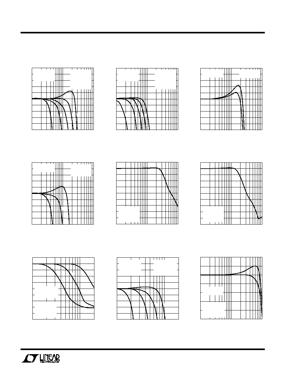
Gain vs Frequency
Phase Factor vs f
CLK
(Typical Unit)
Phase Factor vs f
CLK
(Typical Unit)
Passband Gain and Phase
Passband Gain and Phase
Phase Factor vs f
CLK
(Min and
Max Representative Units)
Phase Factor vs f
CLK
(Min and
Max Representative Units)
f
CLK
(MHz)
0
390
PHASE FACTOR
400
420
430
440
460
1264-7 G02
410
450
2
5
1
3
4
0°C
25°C
V
S
= ±7.5V
(f
CLK
/f
C
) = 25:1
70°C
f
CLK
(MHz)
0
390
PHASE FACTOR 400
380
420
430
450
1264-7 G03
410
440
2
5
1
3
4
370
0°C
25°C
V
S
= ±7.5V
(f
CLK
/f
C
) = 50:1
70°C
f
CLK
(MHz)
0
395
PHASE FACTOR
400
405
410
415
425
0.5
1.0
1.5
2.0
1264-7 G05
2.5
3.0
420
V
S
= ±5V
(f
CLK
/f
C
) = 25:1
T
A
= 25°C
f
CLK
(MHz)
0
395
PHASE FACTOR
405
420
425
440
450
1264-7 G04
415
445
2
5
3
4
435
430
410
400
V
S
= ±7.5V
(f
CLK
/f
C
) = 25:1
T
A
= 25°C
1
FREQUENCY (kHz)
20
GAIN (dB)
1
0
100
1264-7 G06
3
5
30
60
80
0
90
90
180
PHASE (DEG)
10
3
2
1
2
4
6
7
225
270
135
45
45
135
180
40
50
70
90
110
GAIN
PHASE
V
S
= ±7.5V
f
CLK
= 2.5MHz
f
C
= 100kHz
(f
CLK
/f
C
) = 25:1
FREQUENCY (kHz)
10
GAIN (dB)
1
0
50
1264-7 G07
3
5
15
30
40
0
90
90
180
PHASE (DEG)
5
3
2
1
2
4
6
7
225
270
135
45
45
135
180
20
25
35
45
55
PHASE
GAIN
V
S
= ±7.5V
f
CLK
= 2.5MHz
f
C
= 50kHz
(f
CLK
/f
C
) = 50:1
5
LTC1264-7
C
C
HARA TERISTICS
U
W
A
TYPICAL PERFOR
CE
Passband Gain vs f
CLK
Passband Gain vs f
CLK
Passband Gain vs f
CLK
at 85
°
C
Gain vs Frequency
Gain vs Frequency
Passband Gain vs f
CLK
at 85
°
C
Passband Gain vs f
CLK
Maximum Passband vs
Temperature
Gain vs f
CLK
FREQUENCY (kHz)
10
GAIN (dB)
30
10
1264-7 G14
50
70
90
100
40
20
0
60
80
A
C
200
10
V
S
= SINGLE 5V
(f
CLK
/f
C
) = 25:1
AGND = 2V
T
A
= 25°C
B
A. f
CLK
= 0.5MHz
B. f
CLK
= 1MHz
C. f
CLK
= 2MHz
FREQUENCY (kHz)
10
GAIN (dB)
1
3
1264-7 G15
1
3
5
100
0
2
4
2
4
A
200
5
V
S
= SINGLE 5V
(f
CLK
/f
C
) = 25:1
AGND = 2V
T
A
= 25°C
B
C
D
A. f
CLK
= 0.5MHz
B. f
CLK
= 1.0MHz
C. f
CLK
= 1.5MHz
D. f
CLK
= 2.0MHz
FREQUENCY (kHz)
1
5
GAIN (dB)
3
2
1
10
100
1264-7 G16
4
1
0
2
V
S
= SINGLE 5V
f
CLK
= 2MHz
(f
CLK
/f
C
) = 25:1
AGND = 2V
A
A. T
A
= 70°C
B. T
A
= 40°C
B
FREQUENCY (kHz)
10
90
GAIN (dB)
70
50
30
10
100
1000
1264-7 G13
80
60
40
20
0
10
V
S
= ±5V
f
CLK
= 3MHz
(f
CLK
/f
C
) = 25:1
T
A
= 25°C
FREQUENCY (kHz)
10
90
GAIN (dB)
70
50
30
10
100
1000
1264-7 G12
80
60
40
20
0
10
V
S
= ±7.5V
f
CLK
= 5MHz
(f
CLK
/f
C
) = 25:1
T
A
= 25°C
FREQUENCY (kHz)
10
5
GAIN (dB)
3
1
1
3
100
1000
1264-7 G11
4
2
0
2
4
A
V
S
= ±5V
(f
CLK
/f
C
) = 25:1
5
C
A. f
CLK
= 1MHz
B. f
CLK
= 2MHz
C. f
CLK
= 3MHz
B
FREQUENCY (kHz)
10
5
GAIN (dB)
3
1
1
3
100
1000
1264-7 G08
4
2
0
2
4
A
D
C
E
V
S
= ±7.5V
(f
CLK
/f
C
) = 25:1
T
A
= 25°C
5
B
A. f
CLK
= 1MHz
B. f
CLK
= 2MHz
C. f
CLK
= 3MHz
D. f
CLK
= 4MHz
E. f
CLK
= 5MHz
FREQUENCY (kHz)
10
5
GAIN (dB)
3
1
1
3
100
1000
1264-7 G09
4
2
0
2
4
D E
V
S
= ±7.5V
(f
CLK
/f
C
) = 50:1
T
A
= 25°C
5
B
A. f
CLK
= 1MHz
B. f
CLK
= 2MHz
C. f
CLK
= 3MHz
D. f
CLK
= 4MHz
E. f
CLK
= 5MHz
A
C
FREQUENCY (kHz)
10
5
GAIN (dB)
3
1
1
3
100
1000
1264-7 G10
4
2
0
2
4
A
V
S
= ±7.5V
(f
CLK
/f
C
) = 25:1
5
B
A. f
CLK
= 4MHz
B. f
CLK
= 5MHz