Äîêóìåíòàöèÿ è îïèñàíèÿ www.docs.chipfind.ru
1
LTC1164-8
Ultraselective, Low Power
8th Order Elliptic Bandpass Filter
with Adjustable Gain
FEATURES
s
Ultraselectivity
(50dB Attenuation at
±
4% of Center Frequency)
s
Adjustable Passband Gain
s
Noise Independent of Gain
s
Filter Noise: 270
µ
V
RMS
, V
S
= Single 5V Supply
s
Clock-Tunable (Center Frequency = f
CLK
/100)
s
Center Frequencies up to 5kHz, V
S
=
±
5V
(Typical I
SUPPLY
= 3.2mA)
s
Center Frequencies up to 4kHz, V
S
= Single 5V Supply
(Typical I
SUPPLY
= 2.3mA)
DESCRIPTIO
N
U
The LTC
®
1164-8 is a monolithic ultraselective, 8th order,
elliptic bandpass filter. The passband of the LTC1164-8 is
tuned with an external clock and the clock-to-center fre-
quency ratio is 100:1. The 3dB pass bandwidth is typi-
cally 1% of the filter center frequency. The stopband
attenuation of the LTC1164-8 is greater than 50dB. The
lower and upper stopband frequencies are less than
0.96 · center frequency and greater than 1.04 · center
frequency, respectively.
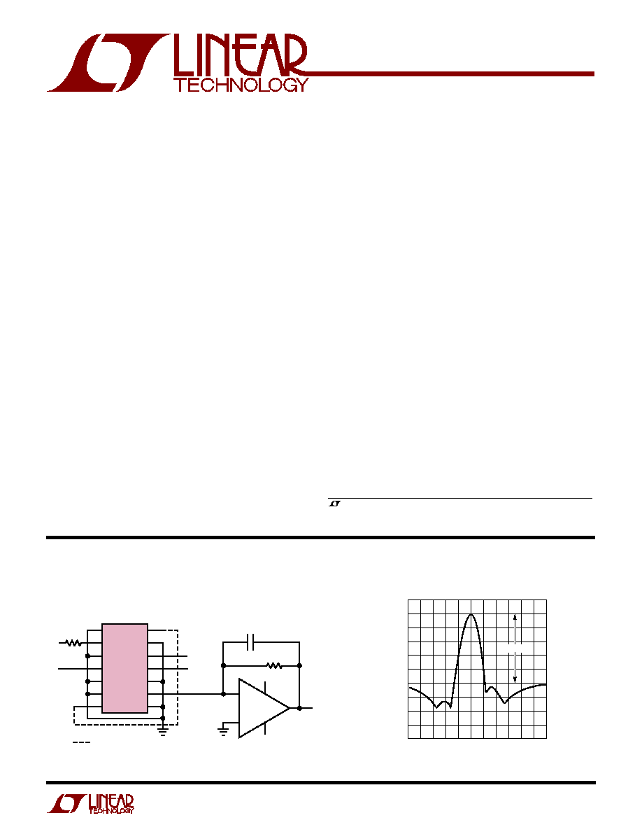
The LTC1164-8 requires an external op amp and two
external resistors (see the circuit below). The filter's gain
at center frequency is set by the ratio R
IN
/R
F
. For a gain
equal to one and an optimum dynamic range, R
F
should be
set to 61.9k and R
IN
should be 340k. For gains other than
one, R
IN
= 340k/Gain. Gains up to 1000 are obtainable.
Setting the filter's gain with input resistor R
IN
does not
increase the filter's wideband noise. The 270
µ
V
RMS
wideband noise of the LTC1164-8 is independent of the
filter's center frequency.
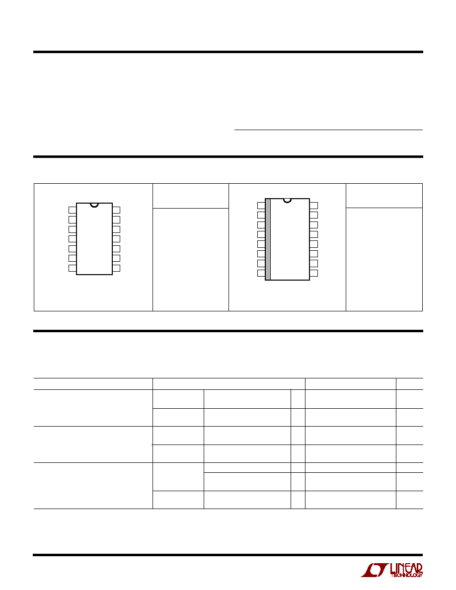
The LTC1164-8 is available in a 14-pin PDIP or a 16-pin
surface mount SO Wide package.
TYPICAL APPLICATIO
N
U
Frequency Response
Ultranarrow 1kHz Bandpass Filter with Gain = 10
Gain = 340k/R
IN
, 1/(2
· R
F
· C
F
)
10 · Center Frequency
LTC1164-8
5V
5V
5V
2
3
4
6
7
V
OUT
LTC1164-8 · TA01
5V
V
IN
R
IN
34k
100kHz
SHORT CONNECTION UNDER IC AND
SHIELDED BY A GROUND PLANE
1
2
3
4
5
6
7
14
13
12
11
10
9
8
R
F
61.9k
C
F
200pF
+
LT
®
1006
FREQUENCY (kHz)
0.90
GAIN (dB)
30
20
10
0
10
20
30
40
50
60
70
1.10
1164-8 TA02
0.95
1.00
1.05
1.15
50dB
APPLICATIO
N
S
U
s
Asynchronous Narrowband Signal Detectors
s
Low Frequency Asynchronous Demodulators
s
Handheld Spectrum Analyzers
s
In-Band Tone Signaling Detectors
, LTC and LT are registered trademarks of Linear Technology Corporation.
2
LTC1164-8
Total Supply Voltage (V
+
to V
)........................... 16.5V
Power Dissipation ............................................. 700mW
Burn-In Voltage ................................................... 16.5V
Voltage at Any Input .... (V
0.3V)
V
IN
(V
+
+ 0.3V)
Operating Temperature Range* .................. 0
°
C to 70
°
C
Storage Temperature Range ................ 65
°
C to 150
°
C
Lead Temperature (Soldering, 10 sec)................. 300
°
C
ABSOLUTE
M
AXI
M
U
M
RATINGS
W
W
W
U
Maximum Clock Frequency
V
S
=
±
7.5V .................................................... 720kHz
V
S
=
±
5V ....................................................... 540kHz
V
S
= Single 5V ............................................... 430kHz
PACKAGE/ORDER I
N
FOR
M
ATIO
N
W
U
U
ORDER PART
NUMBER
ORDER PART
NUMBER
ELECTRICAL CHARACTERISTICS
(See Test Circuit)
T
A
= 25
°
C, Center Frequency = f
CLK
/100, f
CLK
= 100kHz (the clock signal is a TTL or CMOS square wave, clock rise or fall time
1
µ
s),
the AC test signal level is 1V
RMS
for V
S
=
±
5V or 0.5V
RMS
for V
S
=
±
2.375V, unless otherwise specified.
Consult factory for Industrial and Military grade parts.
*For an extended operating temperature range contact LTC Marketing for
details.
PARAMETER
CONDITIONS
MIN
TYP
MAX
UNITS
Gain at Center Frequency
V
S
=
±
2.375V
f
IN
= 1000Hz
3
0
±
1.5
3
dB
q
4
0
±
2.0
4
dB
V
S
=
±
5V
f
IN
= 1000Hz
3
0
±
1.5
3
dB
q
4
0
±
2.0
4
dB
Gain at 0.995 · Center Frequency and
V
S
=
±
2.375V
f
IN
= 995Hz
q
9
3
dB
1.005 · Center Frequency
f
IN
= 1005Hz
q
9
3
dB
(Referenced to Gain at Center Frequency)
V
S
=
±
5V
f
IN
= 995Hz
3
±
2
dB
f
IN
= 1005Hz
3
±
2
dB
Lower Stopband Attenuation
V
S
=
±
2.375V
f
IN
= 960Hz (Note 1)
48
52
dB
(Referenced to Gain at Center Frequency)
f
IN
= 800Hz
50
52
58
dB
q
48
60
dB
V
S
=
±
5V
f
IN
= 960Hz (Note 1)
48
52
dB
f
IN
= 800Hz
52
dB
LTC1164-8CN
T
JMAX
= 110
°
C,
JA
= 65
°
C/ W
T
JMAX
= 110
°
C,
JA
= 85
°
C/ W
1
2
3
4
5
6
7
TOP VIEW
N PACKAGE
14-LEAD PDIP
14
13
12
11
10
9
8
NC
INVB
AGND
V
+
AGND
NC
INVA
R(h, l)
NC
V
f
CLK
NC
I
OUT
NC
1
2
3
4
5
6
7
8
TOP VIEW
SW PACKAGE
16-LEAD PLASTIC SO WIDE
16
15
14
13
12
11
10
9
NC
INVB
AGND
V
+
AGND
NC
NC
INVA
R(h, l)
NC
V
NC
f
CLK
NC
NC
I
OUT
LTC1164-8CSW
3
LTC1164-8
ELECTRICAL CHARACTERISTICS
(See Test Circuit)
PARAMETER
CONDITIONS
MIN
TYP
MAX
UNITS
Upper Stopband Attenuation
V
S
=
±
2.375V
f
IN
= 1040Hz (Note 1)
48
52
dB
(Referenced to Gain at Center Frequency)
f
IN
= 1200Hz
50
52
58
dB
q
48
60
dB
V
S
=
±
5V
f
IN
= 1040Hz (Note 1)
48
52
dB
f
IN
= 1200Hz
52
dB
Maximum Output for < 0.25%
V
S
=
±
2.5V
f
IN
= 1000Hz
1.0
V
RMS
Total Harmonic Distortion
V
S
=
±
5V
f
IN
= 1000Hz
2.5
V
RMS
Output DC Offset
V
S
=
±
2.5V (At the Output of External Op Amp)
40
±
50
mV
V
S
=
±
5V
50
±
60
mV
Power Supply Current (Note 2)
V
S
=
±
2.375V
2.3
4.0
mA
q
4.5
mA
V
S
=
±
5V
3.2
7.0
mA
q
8.0
mA
V
S
=
±
7.5V
4.5
11.0
mA
q
12.5
mA
Power Supply Range
±
2.375
±
8
V
T
A
= 25
°
C, Center Frequency = f
CLK
/100, f
CLK
= 100kHz ( the clock signal is a TTL or CMOS square wave, clock rise or fall time
1
µ
s),
the AC test signal level is 1V
RMS
for V
S
=
±
5V or 0.5V
RMS
for V
S
=
±
2.375V, unless otherwise specified.
The
q
denotes specifications which apply over the full operating
temperature range.
Note 1: The minimum stopband attenuation at 960Hz and 1040Hz is
guaranteed by design and test correlation.
Note 2: The maximum current over temperature is at 0
°
C. At 70
°
C the
maximum current is less than its maximum value at 25
°
C.
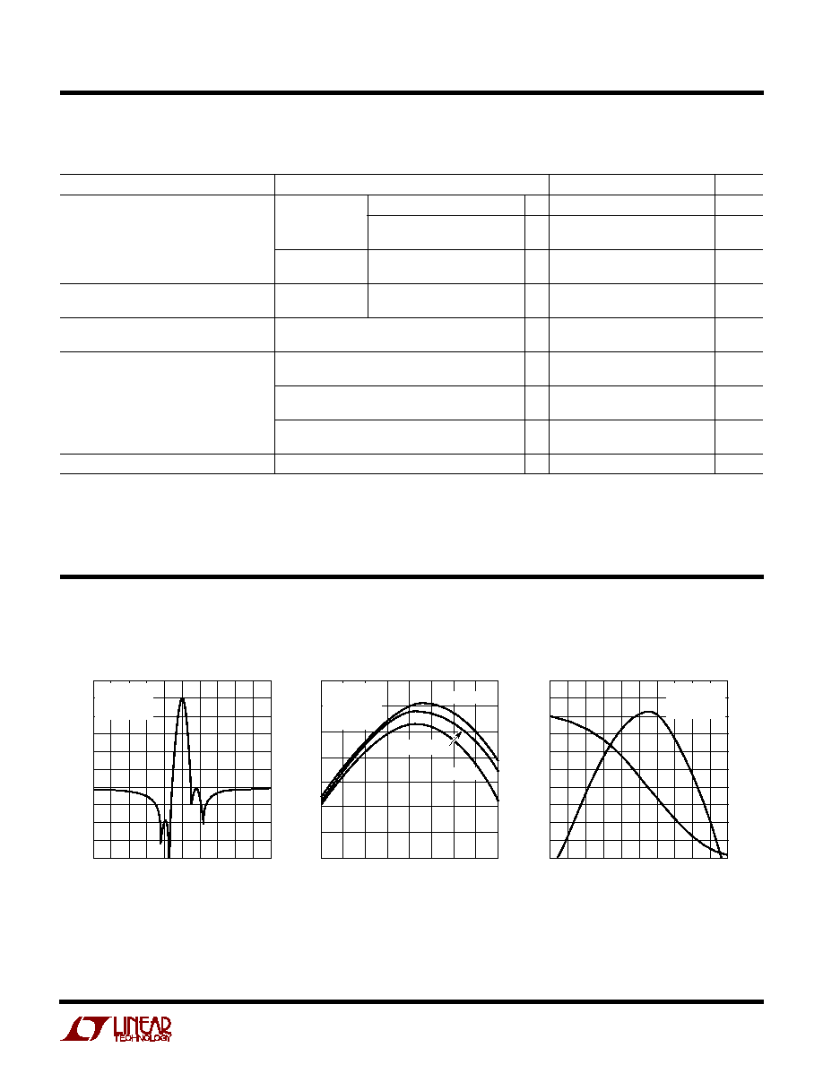
TYPICAL PERFOR
M
A
N
CE CHARACTERISTICS
U
W
FREQUENCY (Hz)
760
GAIN (dB)
30
10
10
1240
LTC1164-8 · TPC01
50
70
40
20
0
60
80
90
880
1000
1120
T
A
= 25
°
C
V
S
=
±
5V
f
CLK
= 100kHz
Gain vs Frequency
Passband Gain and Phase
vs Frequency
Passband Variations
vs Power Supply
FREQUENCY (Hz)
990
GAIN (dB)
6
3
0
1005
LTC1164-8 · TPC02
9
12
995
1000
1010
15
18
3
f
CLK
= 100kHz
GAIN = 1
R
IN
= 340k
R
F
= 61.9k
V
S
=
±
2.5V
V
S
=
±
7.5V
V
S
=
±
5V
FREQUENCY (Hz)
984
GAIN (dB)
PHASE (DEG)
6
0
6
1016
LTC1164-8 · TPC03
12
18
9
3
3
15
21
24
60
60
180
120
180
300
120
0
240
360
420
992
1000
1008
T
A
= 25
°
C
V
S
=
±
5V
f
CLK
= 100kHz
4
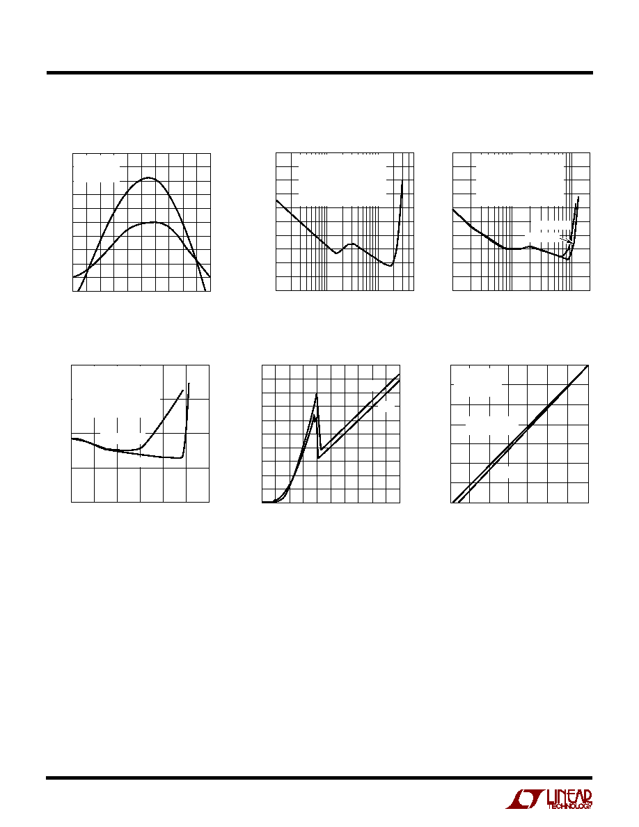
LTC1164-8
TYPICAL PERFOR
M
A
N
CE CHARACTERISTICS
U
W
Passband Gain and Delay
vs Frequency
THD + Noise vs Input Voltage
THD + Noise vs Input Voltage
FREQUENCY (Hz)
984
GAIN (dB)
DELAY (ms)
6
0
6
1016
LTC1164-8 · TPC04
12
18
9
3
3
15
21
24
60
80
100
90
40
20
50
70
30
10
0
992
1000
1008
T
A
= 25
°
C
V
S
=
±
5V
f
CLK
= 100kHz
INPUT VOLTAGE (V
RMS
)
0.01
56
20 LOG (THD + NOISE
/
V
IN
) (dB)
50
44
38
32
0.1
1
5
LTC1164-8 · TPC05
62
68
74
80
26
20
T
A
= 25
°
C
V
S
=
±
5V
f
IN
= 1kHz
f
CLK
= 100kHz
FILTER GAIN AT f
CENTER
= 1
OUTPUT OP AMP IS LT1006
INPUT VOLTAGE (V
RMS
)
0.01
56
20 LOG (THD + NOISE
/
V
IN
) (dB)
50
44
38
32
0.1
1
2
LTC1164-8 · TPC06
62
68
74
80
26
20
T
A
= 25
°
C
V
S
= SINGLE 5V
f
IN
= 1kHz
f
CLK
= 100kHz
FILTER GAIN AT f
CENTER
= 1
OUTPUT OP AMP IS LT1006
AGND = 2.5V
AGND = 2V
INPUT VOLTAGE (V
P-P
)
0.5
80
20 LOG (THD + NOISE
/
V
IN
) (dB)
70
60
50
40
1.0
1.5
2.0
2.5
LTC1164-8 · TPC07
3.0
3.5
AGND AT 2.5V
AGND AT 2V
T
A
= 25
°
C
V
S
= SINGLE 5V
f
IN
= 1kHz
f
CLK
= 100kHz
FILTER GAIN AT f
CENTER
= 1
OUTPUT OP AMP IS LT1006
POWER SUPPLY VOLTAGE (V
+
OR V
)
0
POWER SUPPLY CURRENT (mA)
3.0
4.0
5.0
6.4
LTC1164-8 · TPC08
2.0
1.0
0
1.6
3.2
4.8
0.8
7.2
2.4
4.0
5.6
8.0
25
°
C
70
°
C
Power Supply Current
vs Power Supply Voltage
THD + Noise vs Input Voltage
Output vs Input
INPUT LEVEL (dBV)
60
20
10
10
30
10
LT
C1164-8 · TPC09
30
40
50
40
20
0
10
50
60
0
OUTPUT LEVEL (dBV)
V
S
= SINGLE 5V
(PINS 3, 5 AT 2V)
V
S
=
±
5V
f
CLK
= 100kHz
f
CENTER
= 1kHz
f
IN
= 1kHz
5
LTC1164-8
PI
N
FU
N
CTIO
N
S
U
U
U
1
2
3
4
5
6
7
14
13
12
11
10
9
8
LTC1164-8
R
IN
340k
V
IN
5V
f
CLK
0.1
µ
F
15k
V
OUT
+
1
µ
F
R
F
61.9k
5V
7
4
6
2
3
LTC1164-8 · F02
0.1
µ
F
10k
+
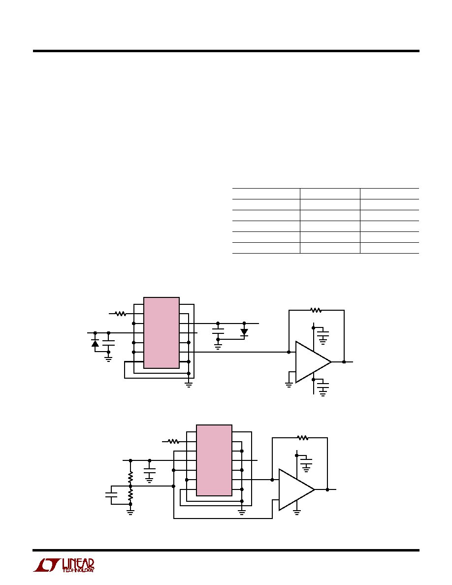
Figure 2. Single Power Supply Operation (Gain = 1)
Figure 1. Dual Power Supply Operation (Gain = 1)
1
2
3
4
5
6
7
14
13
12
11
10
9
8
LTC1164-8
R
IN
340k
V
IN
5V
f
CLK
0.1
µ
F
*FOR SURFACE MOUNT CIRCUITS
USE MOTOROLA DIODE MBR0530
OR EQUIVALENT
0.1
µ
F
*1N4148
OR EQUIVALENT
1N4148*
OR EQUIVALENT
V
OUT
5V
+
R
F
61.9k
5V
7
4
6
2
3
5V
LTC1164-8 · F01
0.1
µ
F
0.1
µ
F
(14-Lead PDIP)
V
+
, V
(Pins 4, 12): Power Supply Pins. The V
+
(Pin 4)
and the V
(Pin 12) should be bypassed with a 0.1
µ
F
capacitor to a reliable ground plane. The filter's power
supplies should be isolated from other digital or high
voltage analog supplies. A low noise linear supply is
recommended. Using a switching power supply will
lower the signal-to-noise ratio of the filter. The power
supply during power-up should have a slew rate of less
than 1V/
µ
s.
For dual supply operation if the V
+
supply is applied before
the V
supply or the V
supply is applied before the V
+
supply, a signal diode on each supply pin to ground will
prevent latchup. Figures 1 and 2 show typical connections
for dual and single supply operation.
f
CLK
(Pin 11): Clock Input Pin. Any TTL or CMOS clock
source with a square wave output and 50% duty cycle
(
±
10%) is an adequate clock source for the device. The
power supply for the clock source should not be the filter's
power supply. The analog ground for the filter should be
connected to the clock's ground at a single point only.
Table 1 shows the clock's low and high level threshold
values for dual or single supply operation. A pulse genera-
tor can be used as a clock source provided the high level
on-time is at least 1
µ
s. Sine waves are not recommended
for clock input frequencies less than 100kHz. The clock's
rise or fall time should be equal to or less than 1
µ
s.
Table 1. Clock Source High and Low Threshold Levels
POWER SUPPLY
HIGH LEVEL
LOW LEVEL
Single Supply = 5V
>1.45V
<0.5V
Single Supply = 12V
>7.80V
<6.5V
Dual Supply =
±
2.5V
>0.73V
< 2.0V
Dual Supply =
±
5V
>1.45V
<0.5V
Dual Supply =
±
7.5V
>2.18V
<0.5V