Äîêóìåíòàöèÿ è îïèñàíèÿ www.docs.chipfind.ru
1
LTC1156
Quad High Side
Micropower MOSFET Driver
with Internal Charge Pump
SUPPLY VOLTAGE (V)
0
0
SUPPLY CURRENT (
µ
A)
10
30
40
50
100
70
5
10
LTC1156 G01
20
80
90
60
15
20
V
IN1
= V
IN2
= V
IN3
= V
IN4
= 0V
T
J
= 25°C
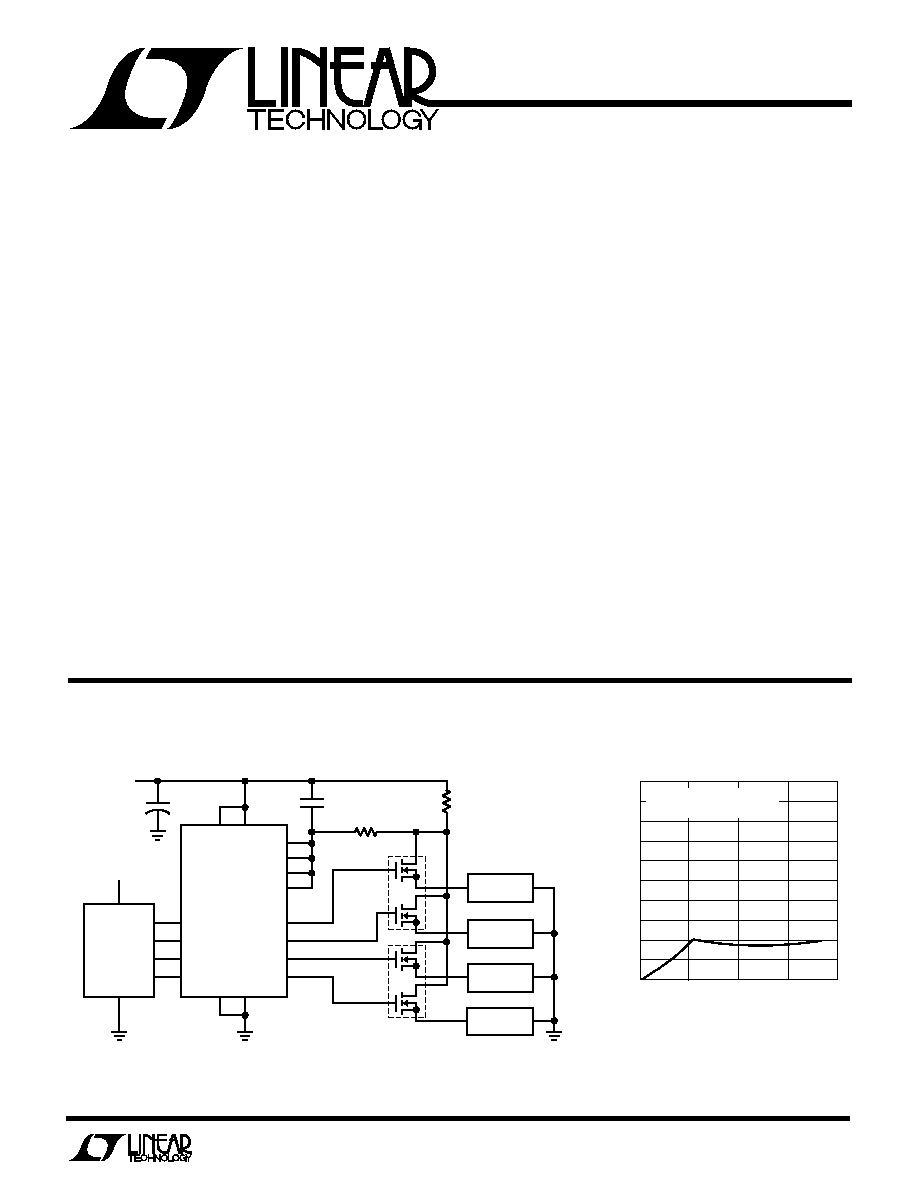
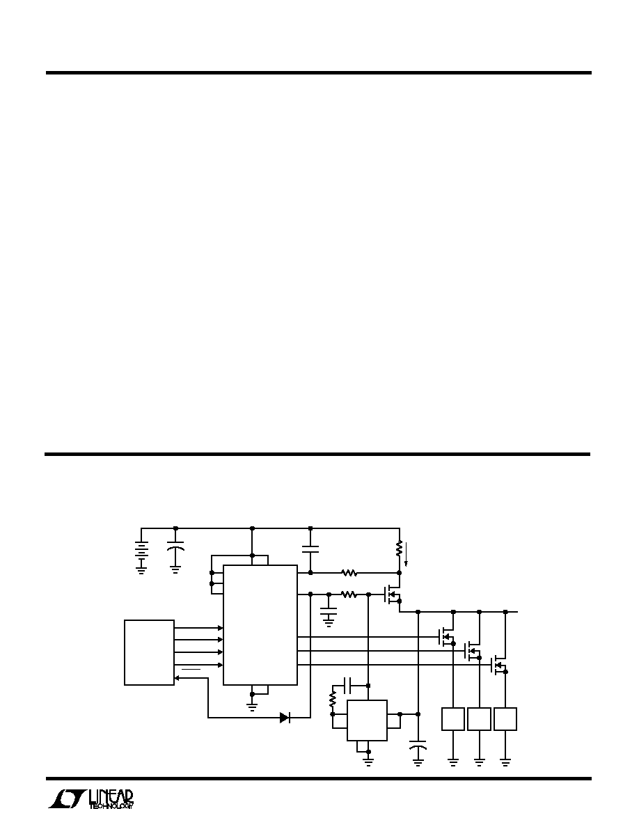
Laptop Computer Power Management
Standby Supply Current
5V
0.1
µ
F
100k
*30m
1156 TA01
ALL COMPONENTS SHOWN ARE SURFACE MOUNT. MINIMUM PARTS COUNT
SHOWN. CURRENT LIMITS CAN BE SET SEPARATELY AND TAILORED TO
INDIVIDUAL LOAD CHARACTERISTICS.
* IMS026 INTERNATIONAL MANUFACTURING SERVICES, INC. (401) 683-9700
V
S
V
S
DS1
DS2
DS3
DS4
IN1
IN2
IN3
IN4
G1
G2
G3
G4
CONTROL
LOGIC
OR
µ
P
+
10
µ
F
5V
Si9956DY
Si9956DY
GND GND
LTC1156
FLOPPY DISK
DRIVE
HARD DISK
DRIVE
DISPLAY
PERIPHERAL
U
A
O
PPLICATI
TYPICAL
D
U
ESCRIPTIO
S
FEATURE
s
No External Charge Pump Components
s
Fully Enhances N-Channel Power MOSFETs
s
16 Microamps Standby Current
s
95 Microamps ON Current
s
Wide Power Supply Range 4.5V to 18V
s
Controlled Switching ON and OFF Times
s
Replaces P-Channel High Side Switches
s
Compatible with Standard Logic Families
s
Available in 16-pin SOL Package
U
S
A
O
PPLICATI
The LTC1156 quad High side gate driver allows using low
cost N-channel FETs for high side switching applications.
An internal charge pump boosts the gate drive voltage
above the positive rail, fully enhancing an N-channel MOS
switch with no external components. Micropower opera-
tion, with 16
µ
A standby current and 95
µ
A operating
current, allows use in virtually all systems with maximum
efficiency.
Included on chip is independent over-current sensing to
provide automatic shutdown in case of short circuits. A
time delay can be added to the current sense to prevent
false triggering on high in-rush current loads.
The LTC1156 operates off of a 4.5V to 18V supply and is
well suited for battery-powered applications, particularly
where micropower "sleep" operation is required.
The LTC1156 is available in both 16-pin DIP and 16-pin
SOL packages.
s
Laptop Computer Power Switching
s
SCSI Termination Power Switching
s
Cellular Telephone Power Management
s
P-Channel Switch Replacement
s
Battery Charging and Management
s
Low Frequency H-Bridge Driver
s
Stepper Motor and DC Motor Control
2
LTC1156
A
U
G
W
A
W
U
W
A
R
BSOLUTE
XI
TI
S
ORDER PART
NUMBER
LTC1156CN
ORDER PART
NUMBER
LTC1156CS
1
2
3
4
5
6
7
8
TOP VIEW
16
15
14
13
12
11
10
9
GND
IN1
V
S
IN2
IN3
GND
IN4
V
S
G1
DS1
G2
DS2
DS3
G3
DS4
G4
N PACKAGE
16-LEAD PLASTIC DIP
TOP VIEW
S PACKAGE
16-LEAD PLASTIC SOL
1
2
3
4
5
6
7
8
16
15
14
13
12
11
10
9
GND
IN1
V
S
IN2
IN3
GND
IN4
V
S
G1
DS1
G2
DS2
DS3
G3
DS4
G4
T
JMAX
=
110
°
C,
JA
=
120
°
C/W
T
JMAX
= 110
°
C,
JA
= 130
°
C/W
Consult factory for Industrial and Military grade parts.
SYMBOL
PARAMETER
CONDITIONS
MIN
TYP
MAX
UNITS
V
S
Supply Voltage
(Note 1)
q
4.5
18
V
I
Q
Quiescent Current OFF
V
S
= 5V, V
IN
= 0V (Note 2)
16
40
µ
A
I
Q
Quiescent Current ON
V
S
= 5V, V
IN
= 5V (Note 3)
95
125
µ
A
I
Q
Quiescent Current ON
V
S
= 12V, V
IN
= 5V (Note 3)
180
400
µ
A
V
INH
Input High Voltage
q
2.0
V
V
INL
Input Low Voltage
q
0.8
V
I
IN
Input Current
0V < V
IN
< V
S
q
±
1.0
µ
A
C
IN
Input Capacitance
5
pF
V
SEN
Drain Sense Threshold
80
100
120
mV
Voltage
q
75
100
125
mV
I
SEN
Drain Sense Input Current
0V < V
SEN
< V
S
q
±
0.1
µ
A
V
GATE
V
S
Gate Voltage Above Supply
V
S
= 5V
q
6.0
7.0
9.0
V
V
S
= 6V
q
7.5
8.3
15.0
V
V
S
= 12V
q
15
18
25
V
t
ON
Turn-ON Time
V
S
= 5V, C
GATE
= 1000pF
Time for V
GATE
> V
S
+ 2V
50
250
750
µ
s
Time for V
GATE
> V
S
+ 5V
200
1100
2000
µ
s
V
S
= 12V, C
GATE
= 1000pF
Time for V
GATE
> V
S
+ 5V
50
180
500
µ
s
Time for V
GATE
> V
S
+ 10V
120
450
1200
µ
s
Supply Voltage ....................................................... 22V
Input Voltage ..................... (V
S
+ 0.3V) to (GND 0.3V)
Gate Voltage ....................... (V
S
+ 24V) to (GND 0.3V)
Current (Any Pin) ................................................. 50mA
Operating Temperature Range
LTC1156C ............................................. 0
°
C to 70
°
C
Storage Temperature Range ................. 65
°
C to 150
°
C
Lead Temperature (Soldering, 10 sec.) ................. 300
°
C
ELECTRICAL C
C
HARA TERISTICS
V
S
= 4.5V to 18V, T
A
= 25
°
C, unless otherwise noted.
W
U
U
PACKAGE/ORDER I FOR ATIO
3
LTC1156
The
q
denotes specifications which apply over the full operating
temperature range.
Note 1: Both V
S
pins (3 and 8) must be connected together, and both
ground pins (1 and 6) must be connected together.
Note 2: Quiescent current OFF is for all channels in OFF condition.
Note 3: Quiescent current ON is per driver and is measured independently.
C
C
HARA TERISTICS
U
W
A
TYPICAL PERFOR
CE
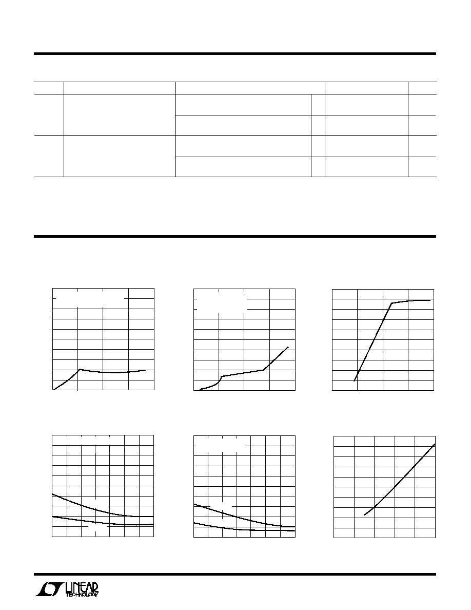
Standby Supply Current
SUPPLY VOLTAGE (V)
0
4
V
GATE
V
S
(V)
6
10
12
14
24
18
5
10
LTC1156 G03
8
20
22
16
15
20
SUPPLY VOLTAGE (V)
0
0
SUPPLY CURRENT (
µ
A)
100
300
400
500
1000
700
5
10
1156 G02
200
800
900
600
15
20
ONE INPUT = ON
OTHER INPUTS = OFF
T
J
= 25°C
Supply Current per Channel ON
High Side Gate Voltage
Standby Supply Current
Supply Current per Channel ON
Low Side Gate Voltage
SUPPLY VOLTAGE (V)
0
V
GATE
(V)
18
24
30
8
1158 G06
12
6
0
2
4
6
10
27
21
15
9
3
SUPPLY VOLTAGE (V)
0
0
SUPPLY CURRENT (
µ
A)
10
30
40
50
100
70
5
10
LTC1156 G01
20
80
90
60
15
20
V
IN1
= V
IN2
= V
IN3
= V
IN4
= 0V
T
J
= 25°C
TEMPERATURE (°C)
50
0
SUPPLY CURRENT (
µ
A)
10
30
40
50
100
70
0
50
75
1156 G04
20
80
90
60
25
25
100
125
V
S
= 18V
V
S
= 5V
V
IN1
= V
IN2
= V
IN3
= V
IN4
= 0V
TEMPERATURE (°C)
50
0
SUPPLY CURRENT (
µ
A)
100
300
400
500
1000
700
0
50
75
1156 G05
200
800
900
600
25
25
100
125
V
S
= 18V
V
S
= 5V
ONE INPUT = ON
OTHER INPUTS = OFF
V
S
= 4.5V to 18V, T
A
= 25
°
C, unless otherwise noted.
SYMBOL
PARAMETER
CONDITIONS
MIN
TYP
MAX
UNITS
t
OFF
Turn-OFF Time
V
S
= 5V, C
GATE
= 1000pF
Time for V
GATE
< 1V
10
36
60
µ
s
V
S
= 12V, C
GATE
= 1000pF
Time for V
GATE
< 1V
10
26
60
µ
s
t
SC
Short Circuit Turn-OFF Time
V
S
= 5V, C
GATE
= 1000pF
Time for V
GATE
< 1V
5
16
30
µ
s
V
S
= 12V, C
GATE
= 1000pF
Time for V
GATE
< 1V
5
16
30
µ
s
ELECTRICAL C
C
HARA TERISTICS
4
LTC1156
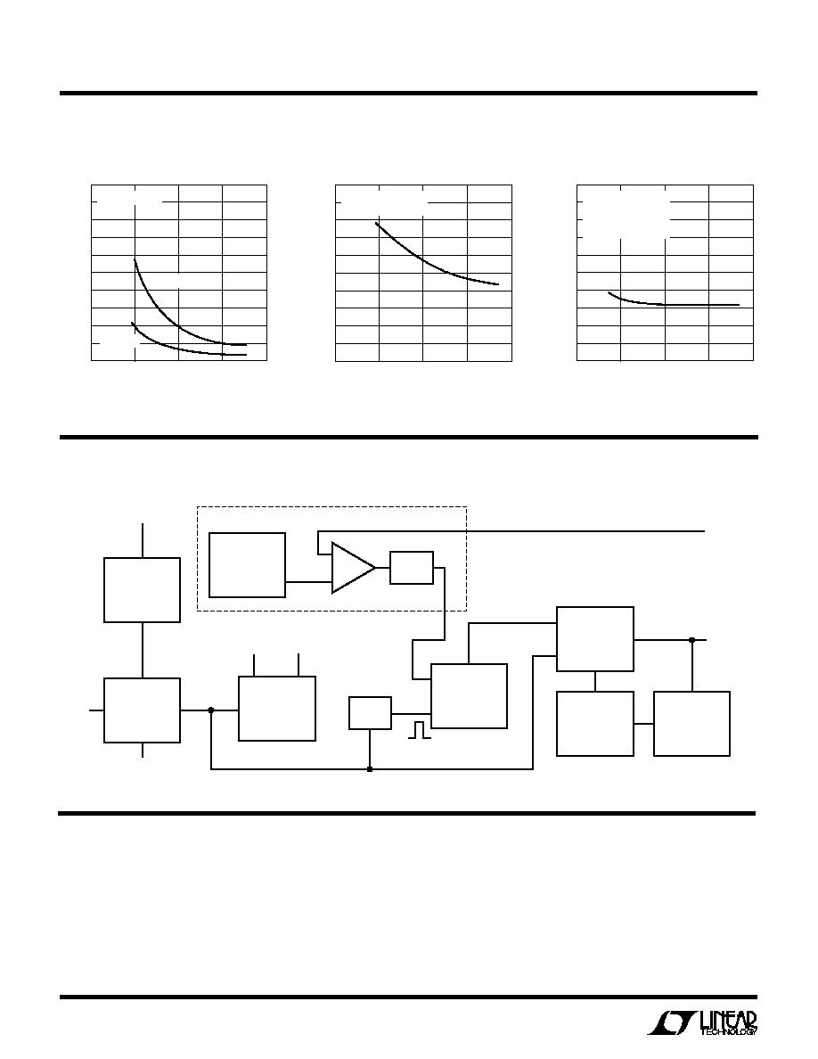
W
I
D AGRA
BLOCK
GATE CHARGE
AND DISCHARGE
CONTROL LOGIC
COMP
LOW STANDBY
CURRENT
REGULATOR
TTL-TO-CMOS
CONVERTER
100mV
REFERENCE
VOLTAGE
REGULATORS
INPUT
LATCH
OSCILLATOR
AND CHARGE
PUMP
FAST/SLOW
GATE CHARGE
LOGIC
V
S
ANALOG SECTION
IN
GND
ANALOG
DIGITAL
10
µ
s
DELAY
GATE
DRAIN
SENSE
ONE
SHOT
R
S
1156 BD
C
C
HARA TERISTICS
U
W
A
TYPICAL PERFOR
CE
SUPPLY VOLTAGE (V)
0
0
TURN-ON TIME (
µ
s)
100
300
400
500
1000
700
5
10
1156 G07
200
800
900
600
15
20
C
GATE
= 1000pF
V
GS
= 5V
V
GS
= 2V
SUPPLY VOLTAGE (V)
0
0
TURN-OFF TIME (
µ
s)
5
15
20
25
50
35
5
10
1156 G08
10
40
45
30
15
20
C
GATE
= 1000pF
TIME FOR V
GATE
< 1V
SUPPLY VOLTAGE (V)
0
0
TURN-OFF TIME (
µ
s)
5
15
20
25
50
35
5
10
1156 G09
10
40
45
30
15
20
C
GATE
= 1000pF
TIME FOR V
GATE
< 1V
V
SEN
= V
S
1V
NO EXTERNAL DELAY
Short Circuit Turn-OFF Delay Time
Turn-OFF Time
Turn-ON Time
U
ATIO
OPER
The LTC1156 contains four independent power MOSFET
gate drivers and protection circuits (refer to the Block
Diagram for detail). Each section of LTC1156 consists of
the following functional blocks:
TTL and CMOS Compatible Inputs
Each driver input has been designed to accommodate a
wide range of logic families. The input threshold is set at
1.3V with approximately 100mV of hysteresis.
5
LTC1156
U
ATIO
OPER
A voltage regulator with low standby current provides
continuous bias for the TTL to CMOS converters. The TTL
to CMOS converter output enables the rest of the circuitry.
In this way the power consumption is kept to a minimum
in the standby mode.
Internal Voltage Regulation
The output of the TTL to CMOS converter drives two
regulated supplies which power the low voltage CMOS
logic and analog blocks. The regulator outputs are isolated
from each other so that the noise generated by the charge
pump logic is not coupled into the 100mV reference or the
analog comparator.
Gate Charge Pump
Gate drive for the power MOSFET is produced by an
adaptive charge pump circuit which generates a gate
voltage substantially higher than the power supply volt-
age. The charge pump capacitors are included on chip and
therefore no external components are required to generate
the gate drive.
Drain Current Sense
The LTC1156 is configured to sense the drain current of
the power MOSFET in high side applications. An internal
100mV reference is compared to the drop across a sense
resistor (typically 0.002
to 0.1
) in series with the drain
lead. If the drop across this resistor exceeds the internal
100mV threshold, the input latch is reset and the gate is
quickly discharged by a large N-channel transistor. A
simple RC network can be added to delay the over-current
protection so that large in-rush current loads such as
lamps or capacitors can be started.
Supply and Ground Pins
The two supply pins (3 and 8) of the LTC1156 must be
connected together at all times and the two ground pins (1
and 6) must be connected together at all times. The two
supply pins should be connected to the "top" of the drain
current sense resistor/s to ensure accurate sensing.
For further applications information, see the LTC1155
Dual High Side Micropower MOSFET Driver data sheet.
U
S
A
O
PPLICATI
TYPICAL
4-Cell Extremely Low Voltage Drop Regulator and Three Load
Switches with Short-Circuit Protection and 20
µ
A Standby Current
V
S
V
S
DS2
DS3
DS4
IN1
IN2
IN3
IN4
G2
G3
G4
GND GND
LTC1156
+
+
CONTROL
LOGIC
DS1
G1
REG ON/OFF
FAULT
1N4148
0.1
µ
F
100k
100k
5.2V TO 6V
4-CELL NiCd
BATTERY PACK
47
µ
F
0.1
µ
F
**0.03
3.3A MAX
5V/2A
SWITCHED
2
×
Si9956DY
200pF
1
3
4
5
6
7
8
10k
LT1431
*470
µ
F
5V
LOAD
5V
LOAD
5V
LOAD
1156 TA02
+
* CAPACITOR ESR LESS THAN 0.5
** RCS02 ULTRONIX (303) 242-0810
IRLR024