
1
LTC1154
D
U
ESCRIPTIO
S
FEATURE
High-Side Micropower
MOSFET Driver
s
Fully Enhances N-Channel Power MOSFETs
s
8
Á
A I
Q
Standby Current
s
85
Á
A I
Q
ON Current
s
No External Charge Pump Capacitors
s
4.5V to 18V Supply Range
s
Short-Circuit Protection
s
Thermal Shutdown via PTC Thermistor
s
Status Output Indicates Shutdown
s
Available in 8-Pin SOIC
The LTC1154 single high-side gate driver allows using low
cost N-channel FETs for high-side switching applications.
An internal charge pump boosts the gate drive voltage
above the positive rail, fully enhancing an N-channel MOS
switch with no external components. Micropower opera-
tion, with 8
Á
A standby current and 85
Á
A operating cur-
rent, allows use in virtually all systems with maximum
efficiency.
Included on chip is programmable over-current sensing.
A time delay can be added to prevent false triggering on
high in-rush current loads. An active high shutdown input
is also provided and interfaces directly to a standard PTC
thermistor for thermal shutdown. An open-drain output is
provided to report switch status to the
Á
P. An active low
enable input is provided to control multiple switches in
banks.
The LTC1154 is available in both 8-pin DIP and 8-pin SOIC
packages.
U
A
O
PPLICATI
TYPICAL
U
S
A
O
PPLICATI
s
Laptop Computer Power Switching
s
SCSI Termination Power Switching
s
Cellular Telephone Power Management
s
Battery Charging and Management
s
High-Side Industrial and Automotive Switching
s
Stepper Motor and DC Motor Control
Standby Supply Current
Ultra-Low Voltage Drop High-Side Switch
with Short-Circuit Protection
SUPPLY VOLTAGE (V)
0
0
SUPPLY CURRENT (
Á
A)
5
15
20
25
50
35
5
15
LTC1153 Ě TA02
10
40
45
30
10
20
V
IN
= 0V
T
J
= 25░C
IRLR024
0.036
*
LTC1154 Ě TA01
5V
LOAD
Á
P
5V
200k**
0.1
Á
F**
2.7A MAX
51k
IN
EN
STATUS
GND
V
S
DS
G
SD
LTC1154
ALL COMPONENTS SHOWN ARE SURFACE MOUNT.
IMS026 INTERNATIONAL MANUFACTURING SERVICE, INC. (401) 683-9700
NOT REQUIRED IF LOAD IS RESISTIVE OR INDUCTIVE.
*
**

2
LTC1154
A
U
G
W
A
W
U
W
A
R
BSOLUTE
XI
TI
S
Supply Voltage ........................................................ 22V
Input Voltage ..................... (V
S
+ 0.3V) to (GND ş 0.3V)
Enable Input Voltage .......... (V
S
+ 0.3V) to (GND ş 0.3V)
Gate Voltage ....................... (V
S
+ 24V) to (GND ş 0.3V)
Status Output Voltage .............................................. 15V
Current (Any Pin) .................................................. 50mA
Operating Temperature
LTC1154C .............................................. 0
░
C to 70
░
C
Storage Temperature Range ................. ş 65
░
c to 150
░
C
Lead Temperature (Soldering, 10 sec.)................ 300
░
C
LTC1154C
SYMBOL
PARAMETER
CONDITIONS
MIN
TYP
MAX
UNITS
V
S
Supply Voltage
q
4.5
18.0
V
I
Q
Quiescent Current OFF
V
S
= 5V, V
IN
= 0V
8
20
Á
A
I
Q
Quiescent Current ON
V
S
= 5V, V
IN
= 5V
85
120
Á
A
I
Q
Quiescent Current ON
V
S
= 12V, V
IN
= 5V
180
400
Á
A
V
INH
Input High Voltage
q
2
V
V
INL
Input Low Voltage
q
0.8
V
I
IN
Input Current
0V < V
IN
< V
S
q
▒
1
Á
A
C
IN
Input Capacitance
5
pF
V
ENH
ENABLE Input High Voltage
q
3.5
2.6
V
V
ENL
ENABLE Input Low Voltage
q
1.0
0.6
V
I
EN
ENABLE Input Current
0V < V
IN
< V
S
q
▒
1
Á
A
V
SDH
Shutdown Input High Voltage
q
2
V
V
SDL
Shutdown Input Low Voltage
q
0.8
V
I
SD
Shutdown Input Current
0V < V
IN
< V
S
q
▒
1
Á
A
V
SEN
Drain Sense Threshold Voltage
80
100
120
mV
q
75
100
125
mV
I
SEN
Drain Sense Input Current
0V < V
SEN
< V
S
q
▒
0.1
Á
A
W
U
U
PACKAGE/ORDER I FOR ATIO
ORDER PART
NUMBER
S8 PART MARKING
ORDER PART
NUMBER
LTC1154CN8
T
JMAX
= 100
░
C,
JA
= 130
░
C/W (N8)
ELECTRICAL CHARACTERISTICS
V
S
= 4.5V to 18V, T
A
= 25
░
C, V
EN
= 0V, V
SD
= 0V unless otherwise noted.
1154
1
2
3
4
8
7
6
5
TOP VIEW
V
S
DRAIN SENSE
GATE
SHUTDOWN
N8 PACKAGE
8-LEAD PLASTIC DIP
LTC1154 Ě PO01
IN
ENABLE
STATUS
GND
1
2
3
4
8
7
6
5
TOP VIEW
V
S
DRAIN SENSE
GATE
SHUTDOWN
S8 PACKAGE
8-LEAD PLASTIC SOIC
IN
LTC1154 Ě PO02
ENABLE
STATUS
GND
T
JMAX
= 100
░
C,
JA
= 150
░
C/W
LTC1154CS8

3
LTC1154
LTC1154C
SYMBOL
PARAMETER
CONDITIONS
MIN
TYP
MAX
UNITS
V
GATE
ş V
S
Gate Voltage Above Supply
V
S
= 5V
q
6.0
7.0
9.0
V
V
S
= 6V
q
7.5
8.3
15.0
V
V
S
= 12V
q
15.0
18.0
25.0
V
V
STAT
Status Output Low Voltage
I
STAT
= 400
Á
A
q
0.05
0.4
V
I
STAT
Status Output Leakage Current
V
STAT
= 12V
q
1
Á
A
t
ON
Turn-ON Time
V
S
= 5V, C
GATE
= 1000pF
Time for V
GATE
> V
S
+ 2V
30
110
300
Á
s
Time for V
GATE
> V
S
+ 5V
100
450
1000
Á
s
V
S
= 12V, C
GATE
= 1000pF
Time for V
GATE
> V
S
+ 5V
20
80
200
Á
s
Time for V
GATE
> V
S
+ 10V
50
160
500
Á
s
t
OFF
Turn-OFF Time
V
S
= 5V, C
GATE
= 1000pF
Time for V
GATE
< 1V
10
36
60
Á
s
V
S
= 12V, C
GATE
= 1000pF
Time for V
GATE
< 1V
10
28
60
Á
s
t
SC
Short-Circuit Turn-OFF Time
V
S
= 5V, C
GATE
= 1000pF
Time for V
GATE
< 1V
5
25
40
Á
s
V
S
= 12V, C
GATE
= 1000pF
Time for V
GATE
< 1V
5
23
40
Á
s
t
SD
Shutdown Turn-OFF Time
V
S
= 5V, C
GATE
= 1000pF
Time for V
GATE
< 1V
17
40
Á
s
V
S
= 12V, C
GATE
= 1000pF
Time for V
GATE
< 1V
13
35
Á
s
ELECTRICAL CHARACTERISTICS
V
S
= 4.5V to 18V, T
A
= 25
░
C, V
EN
= 0V, V
SD
= 0V unless otherwise noted.
The
q
denotes specifications which apply over the operating temperature range.
C
C
HARA TERISTICS
U
W
A
TYPICAL PERFOR
CE
Standby Supply Current
Supply Current ON
High-Side Gate Voltage
SUPPLY VOLTAGE (V)
0
0
SUPPLY CURRENT (
Á
A)
5
15
20
25
50
35
5
15
LTC1154 Ě TPC01
10
40
45
30
10
20
V
IN
= 0V
T
A
= 25░C
SUPPLY VOLTAGE (V)
0
0
SUPPLY CURRENT (
Á
A)
100
300
400
500
1000
700
5
10
LTC1154 Ě TPC02
200
800
900
600
15
20
T
A
= 25░C
SUPPLY VOLTAGE (V)
0
0
V
GATE
ş V
S
(V)
6
10
12
14
24
18
5
10
LTC1154 Ě TPC03
8
20
22
16
15
20
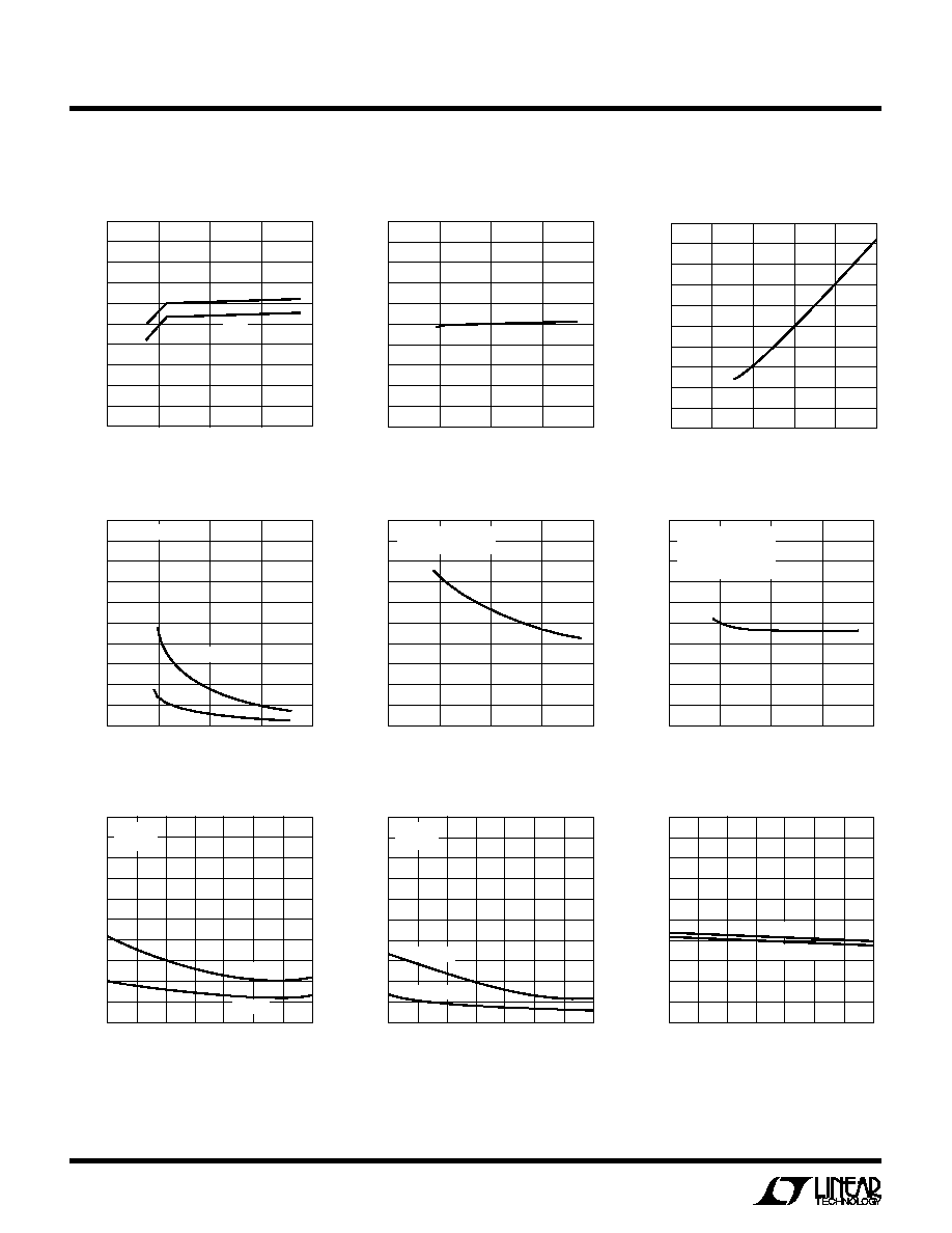
4
LTC1154
C
C
HARA TERISTICS
U
W
A
TYPICAL PERFOR
CE
Input Threshold Voltage
Drain Sense Threshold Voltage
Low-Side Gate Voltage
Supply Current ON
Input ON Threshold Voltage
Turn-ON Time
Standby Supply Current
SUPPLY VOLTAGE (V)
0
0.4
INPUT THRESHOLD VOLTAGE (V)
0.6
1.0
1.2
1.4
2.4
1.8
5
10
LTC1154 Ě TPC04
0.8
2.0
2.2
1.6
15
20
V
ON
V
OFF
SUPPLY VOLTAGE (V)
0
50
DRAIN SENSE THRESHOLD VOLTAGE (V)
60
80
90
100
150
120
5
10
LTC1154 Ě TPC05
70
130
140
110
15
20
SUPPLY VOLTAGE (V)
0
V
GATE
(V)
15
21
27
8
LTC1154 Ě TPC06
9
3
0
2
4
6
10
18
24
30
12
6
Turn-OFF Time
Short-Circuit Turn-OFF Delay Time
TEMPERATURE (░C)
ş50
0
SUPPLY CURRENT (
Á
A)
5
15
20
25
50
35
0
50
75
LTC1154 Ě TPC10
10
40
45
30
ş25
25
100
125
V
S
= 18V
V
S
= 5V
V
IN
= 0V
V
EN
= 0V
TEMPERATURE (░C)
ş50
0
SUPPLY CURRENT (
Á
A)
100
300
400
500
1000
700
0
50
75
LTC1154 Ě TPC11
200
800
900
600
ş25
25
100
125
V
S
= 12V
V
S
= 5V
V
IN
= 5V
V
EN
= 0V
TEMPERATURE (░C)
ş50
0.4
INPUT THRESHOLD VOLTAGE (V)
0.6
1.O
1.2
1.4
2.4
1.8
0
50
75
LTC1154 Ě TPC12
0.8
2.0
2.2
1.6
ş25
25
100
125
V
S
= 18V
V
S
= 5V
SUPPLY VOLTAGE (V)
0
0
TURN-ON TIME (
Á
s)
100
300
400
500
1000
700
5
10
LTC1153 Ě TPC07
200
800
900
600
15
20
V
GS
= 5V
V
GS
= 2V
C
GATE
= 1000pF
SUPPLY VOLTAGE (V)
0
0
TURN-OFF TIME (
Á
s)
5
15
20
25
50
35
5
15
LTC1154 Ě TPC08
10
40
45
30
10
20
C
GATE
= 1000pF
TIME FOR V
GATE
< 1V
SUPPLY VOLTAGE (V)
0
0
TURN-OFF TIME (
Á
s)
5
15
20
25
50
35
5
15
LTC1154 Ě TPC09
10
40
45
30
10
20
C
GATE
= 1000pF
TIME FOR V
GATE
< 1V
V
SEN
= V
S
ş 1V
NO EXTERNAL DELAY
5
LTC1154
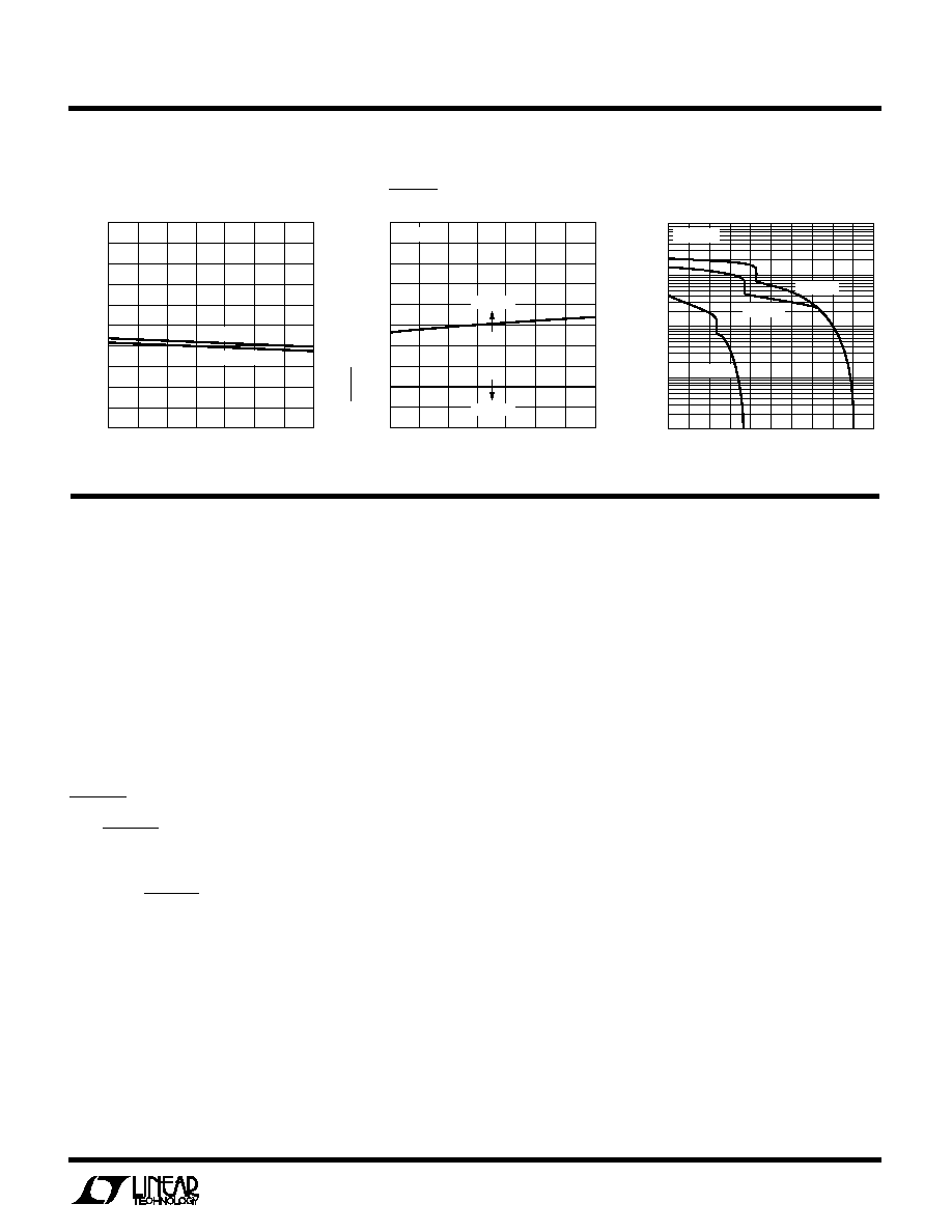
ENABLE Threshold Voltage
Shutdown Threshold Voltage
Gate Drive Current
C
C
HARA TERISTICS
U
W
A
TYPICAL PERFOR
CE
PI FU CTIO S
U
U
U
Input and Shutdown Pins
The LTC1154 input pin is active high and activates all of the
protection and charge pump circuitry when switched ON.
The shutdown pin is designed to immediately disable the
switch if a secondary fault condition (over temperature,
etc.) is detected. The LTC1154 logic and shutdown inputs
are high impedance CMOS gates with ESD protection
diodes to ground and supply and therefore should not be
forced beyond the power supply rails. The shutdown pin
should be connected to ground when not in use.
ENABLE Input Pin
The ENABLE input can be used to enable a number of
LTC1154 high-side switches in banks or to provide a
secondary means of control. It can also act as an inverting
input. The ENABLE input is a high impedance CMOS gate
with ESD clamp diodes to ground and supply and there-
fore should not be forced beyond the power supply rails.
This pin should be grounded when not in use.
Gate Drive Pin
The gate drive pin is either driven to ground when the
switch is turned OFF or driven above the supply rail when
the switch is turned ON. This pin is a relatively high
impedance when driven above the rail (the equivalent of a
few hundred k
). Care should be taken to minimize any
loading of this pin by parasitic resistance to ground or
supply.
Supply Pin
The supply pin of the LTC1154 serves two vital purposes.
The first is obvious: it powers the input, gate drive, regu-
lation and protection circuitry. The second purpose is less
obvious: it provides a Kelvin connection to the top of the
drain sense resistor for the internal 100mV reference.
The LTC1154 is designed to be continuously powered so
that the gate of the MOSFET is actively driven at all times.
If it is necessary to remove power from the supply pin and
then re-apply it, the input pin (or enable pin) should be
cycled a few milliseconds
after the power is re-applied to
reset the input latch and protection circuitry. Also, the
input and enable pins should be isolated with 10k resistors
to limit the current flowing through the ESD protection
diodes to the supply pin.
The supply pin of the LTC1154 should never be forced
below ground as this may result in permanent damage to
the device. A 300
resistor should be inserted in series
with the ground pin if negative supply voltage transients
are anticipated.
TEMPERATURE (░C)
ş50
0.4
SHUTDOWN THRESHOLD VOLTAGE (V) 0.6
1.O
1.2
1.4
2.4
1.8
0
50
75
LTC1154 Ě TPC13
0.8
2.0
2.2
1.6
ş25
25
100
125
V
S
= 18V
V
S
= 5V
TEMPERATURE (░C)
ş50
0
0.5
1.5
2.0
2.5
5.0
3.5
0
50
75
LTC1154 Ě TPC14
1.0
4.0
4.5
3.0
ş25
25
100
125
V
S
= 12V
DISABLE
ENABLE
ENABLE THRESHOLD VOLTAGE (V)
GATE VOLTAGE ABOVE SUPPLY (V)
1
GATE DRIVE CURRENT (
Á
A)
10
100
1000
0
8
12
16
0.1
4
20
LTC1154 Ě TPC15
V
S
= 18V
T
A
= 25░C
V
S
= 12V
V
S
= 5V