
LTC1064-1
1
10641fa
APPLICATIO S
U
FEATURES
DESCRIPTIO
U
TYPICAL APPLICATIO
U
8th Order Filter in a 14-Pin Package
No External Components
100:1 Clock to Center Ratio
150µV
RMS
Total Wideband Noise
0.03% THD or Better
50kHz Maximum Corner Frequency
Operates from ±2.37V to ±8V Power Supplies
Passband Ripple Guaranteed Over Full Military
Temperature Range
Low Noise, 8th Order, Clock
Sweepable Elliptic Lowpass Filter
The LTC
®
1064-1 is an 8th order, clock sweepable elliptic
(Cauer) lowpass switched capacitor filter. The passband
ripple is typically ±0.15dB, and the stopband attenuation
at 1.5 times the cutoff frequency is 68dB or more.
An external TTL or CMOS clock programs the value of the
filter's cutoff frequency. The clock to cutoff frequency ratio
is 100:1.
No external components are needed for cutoff frequencies
up to 20kHz. For cutoff frequencies over 20kHz two low
value capacitors are required to maintain passband flatness.
The LTC1064-1 features low wideband noise and low
harmonic distortion even for input voltages up to 3V
RMS
.
In fact the LTC1064-1 overall performance completes with
equivalent multiple op amp RC active realizations.
The LTC1064-1 is available in a 14-pin DIP or 16-pin
surface mounted SW package.
The LTC1064-1 is pin compatible with the LTC1064-2.
, LTC and LT are registered trademarks of Linear Technology Corporation.
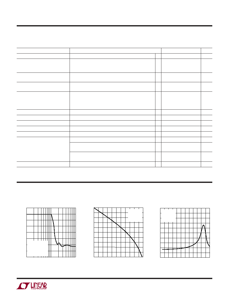
8th Order Clock Sweepable Lowpass
Elliptic Antialiasing Filter
Frequency Response
V
OUT
/V
IN
(dB)
15
0
15
30
45
60
75
90
105
FREQUENCY (kHz)
0
40
1064 TA02
10
5
15
25
35
20
30
8th ORDER CLOCK SWEEPABLE LOWPASS ELLIPTIC ANTIALIASING
FILTER MAINTAINS, FOR 0.1Hz f
CUTOFF
10kHz, A ±0.15dB PASSBAND
RIPPLE AND 72dB STOPBAND ATTENUATION AT 1.5 × f
CUTOFF
.
TOTAL WIDEBAND NOISE = 150µV
RMS
, THD = 0.03% FOR V
IN
= 1V
RMS
LTC1064-1
1
2
3
4
5
6
7
14
13
12
11
10
9
8
R(h, I)
COMP2*
V
f
CLK
NC
V
OUT
NC
INV C
V
IN
AGND
V
+
AGND
COMP1*
INV A
1064 TA01
NOTE: THE POWER SUPPLIES SHOULD BE BYPASSED BY A 0.1µF
CAPACITOR CLOSE TO THE PACKAGE.
FOR SERVO OFFSET NULLING APPLICATIONS, PIN 1 IS THE 2ND
STAGE SUMMING JUNCTION.
*FOR CUTOFF FREQUENCY ABOVE 20kHz, USE COMPENSATION
CAPACITORS (5pF TO 56pF) BETWEEN PIN 13 AND PIN 1
AND PIN 6 AND PIN 7.
CLOCK
(TTL, 5MHz)
8V
8V
V
OUT
V
IN
0.1µF
0.1µF
Antialiasing Filters
Telecom PCM Filters

LTC1064-1
2
10641fa
Total Supply Voltage (V
+
to V
) ............................ 16.5V
Power Dissipation .............................................. 400mW
Storage Temperature Range ................. 65°C to 150°C
Lead Temperature (Soldering, 10 sec).................. 300°C
ORDER PART
NUMBER
LTC1064-1CN
LTC1064-1ACN
ABSOLUTE AXI U
RATI GS
W
W
W
U
PACKAGE/ORDER I FOR ATIO
U
U
W
(Note 1)
1
2
3
4
5
6
7
TOP VIEW
J PACKAGE
14-LEAD CERDIP
N PACKAGE
14-LEAD PDIP
14
13
12
11
10
9
8
INV C
V
IN
AGND
V
+
AGND
COMP1
INV A
R(h, l)
COMP2
V
f
CLK
NC
V
OUT
NC
Operating Temperature Range
LTC1064-1M (OBSOLETE) ............... 55°C to 125°C
LTC1064-1C/AC .................................. 40°C to 85°C
ORDER PART
NUMBER
LTC1064-1CSW
T
JMAX
= 150°C,
JA
= 90°C/W
T
JMAX
= 110°C,
JA
= 70°C/W
LTC1064-1MJ
LTC1064-1CJ
Consult LTC Marketing for parts specified with wider operating temperature ranges.
ELECTRICAL CHARACTERISTICS
The
denotes the specifications which apply over the full operating
temperature range, otherwise specifications are at T
A
= 25°C. V
S
= ±7.5V, f
CLK
= 1MHz, R1 = 10k, C1 = 10pF, TTL or CMOS clock input
level unless otherwise specified.
OBSOLETE PACKAGE
Consider the N14 Package for Alternate Source
1
2
3
4
5
6
7
8
TOP VIEW
SW PACKAGE
16-LEAD PLASTIC (WIDE) SO
16
15
14
13
12
11
10
9
INV C
V
IN
AGND
V
+
AGND
NC
COMP1
INV A
R(h, l)
COMP2
V
NC
f
CLK
NC
NC
V
OUT
PARAMETER
CONDITIONS
MIN
TYP
MAX
UNITS
Passband Gain, LTC1064-1, 1A
Referenced to 0dB, 1Hz to 0.1f
C
± 0.1
± 0.35
dB
Gain TempCo
0.0002
dB/°C
Passband Edge Frequency, f
C
10 ± 1%
kHz
Gain at f
C
Referenced to Passband Gain
LTC1064-1
1.25
0.85
dB
LTC1064-1A
0.75
0.65
dB
3dB Frequency
10.7
kHz
Passband Ripple (Note 1)
0.1f
C
to 0.85f
C
Referenced to Passband Gain,
LTC1064-1
Measured at 6.25kHz and 8.5kHz
± 0.15
± 0.32
dB
LTC1064-1A
± 0.1
± 0.19
dB
Ripple TempCo
0.0004
dB/°C
Stopband Attenuation
At 1.5f
C
Referenced to 0dB
LTC1064-1
66
72
dB
LTC1064-1A
68
72
dB
Stopband Attenuation
At 2f
C
Referenced to 0dB
LTC1064-1
67
72
dB
LTC1064-1A
68
72
dB
LTC1064-1
3
10641fa
ELECTRICAL CHARACTERISTICS
The
denotes the specifications which apply over the full operating
temperature range, otherwise specifications are at T
A
= 25°C. V
S
= ±7.5V, f
CLK
= 1MHz, R1 = 10k, C1 = 10pF, TTL or CMOS clock input
level unless otherwise specified.
Note 2: For tighter specifications please contact LTC Marketing.
PARAMETER
CONDITIONS
MIN
TYP
MAX
UNITS
Input Frequency Range
0
f
CLK
/2
kHz
Output Voltage Swing and
V
S
= ±2.37V
±1
V
Operating Input Voltage Range
V
S
= ±5V
±3
V
V
S
= ±7.5V
±5
V
Total Harmonic Distortion
V
S
= ±5V, Input = 1V
RMS
at 1kHz
0.015
%
V
S
= ±7.5V, Input = 3V
RMS
at 1kHz
0.03
%
Wideband Noise
V
S
= ±5V, Input = GND 1Hz to 999kHz
150
µV
RMS
V
S
= ±7.5V, Input = GND 1Hz to 999kHz
165
µV
RMS
Output DC Offset
V
S
= ±7.5V, Pin 2 Grounded
LTC1064-1
50
175
mV
LTC1064-1A
50
125
mV
Output DC Offset TempCo
V
S
= ±5V
100
µV/°C
Input Impedance
10
20
k
Output Impedance
f
OUT
= 10kHz
2
Output Short-Circuit Current
Source/Sink
3/1
mA
Clock Feedthrough
200
µV
RMS
Maximum Clock Frequency
50% Duty Cycle, V
S
= ±7.5V
5
MHz
Power Supply Current
V
S
= ±2.37V
10
22
mA
V
S
= ±5V
12
23
mA
26
mA
V
S
= ±7.5V, f
CLK
= 1MHz
16
28
mA
32
mA
Power Supply Voltage Range
±2.37
±8
V
FREQUENCY (kHz)
1
GAIN (dB)
15
0
15
30
45
60
75
90
105
10
100
1064 G01
V
S
= ±5V
T
A
= 25°C
f
CLK
= 1MHz
f
C
= 10kHz ± 0.1dB
f
3dB
= 10.7kHz
Note 1: Absolute Maximum Ratings are those values beyond which the life
of a device may be impaired.
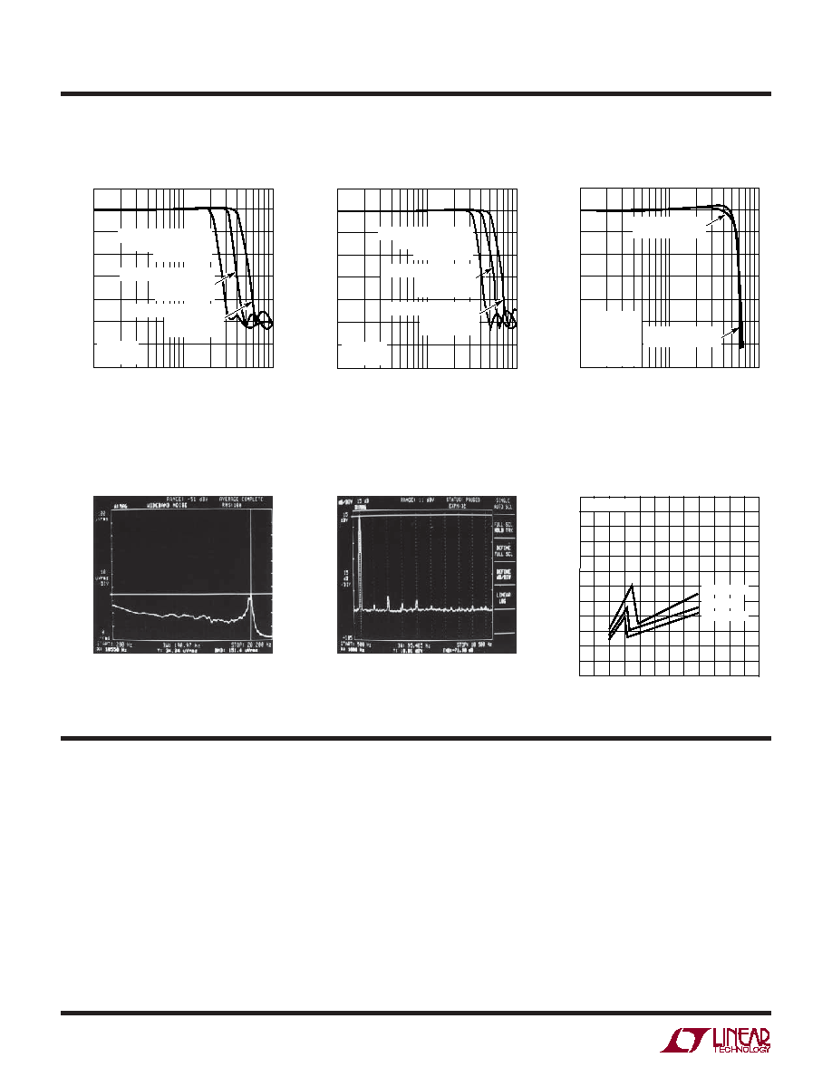
TYPICAL PERFOR A CE CHARACTERISTICS
U
W
Gain vs Frequency
Phase vs Frequency
Group Delay
FREQUENCY (kHz)
0
1
3
5
6
PHASE (DEG)
0
45
90
135
180
225
270
315
360
405
450
10
9
1064 G02
2
4
8
7
11
V
S
= ±5V
T
A
= 25°C
f
CLK
= 1MHz
f
C
= 10kHz
FREQUENCY (kHz)
500
450
400
350
300
250
200
150
100
50
0
GROUP DELAY (
µ
s)
1064 G03
0
1
2
3
4
5
6
7
8
9
12
10 11
V
S
= ±5V
T
A
= 25°C
f
CLK
= 1MHz
f
C
= 10kHz
LTC1064-1
4
10641fa
FREQUENCY (kHz)
1
GAIN (dB)
15
0
15
30
45
60
75
90
105
10
100
1064 G04
f
CLK
= 2MHz, f
C
= 20kHz
COMP1 NOT USED,
COMP2 = 20pF
f
CLK
= 4MHz, f
C
= 40kHz
COMP1 = 36pF
COMP2 = 47pF
f
CLK
= 3MHz, f
C
= 30kHz
COMP1 = 24pF
COMP2 = 36pF
V
S
= ±5V
T
A
= 25°C
FREQUENCY (kHz)
1
GAIN (dB)
15
0
15
30
45
60
75
90
105
10
100
1064 G05
f
CLK
= 3MHz, f
C
= 30kHz
COMP1 = 10pF
COMP2 = 15pF
f
CLK
= 4MHz, f
C
= 40kHz
COMP1 = 20pF
COMP2 = 30pF
V
S
= ±7.5V
T
A
= 25°C
f
CLK
= 5MHz, f
C
= 50kHz
COMP1 = 30pF
COMP2 = 47pF
Gain vs Frequency
Gain vs Frequency
Gain vs Frequency
Typical Wideband Noise
(151µV
RMS
) V
S
= ±5V, T
A
= 25°C
f
CLK
= 1MHz, f
C
= 10kHz Input
Grounded
Power Supply Current vs Power
Supply Voltage
TYPICAL PERFOR A CE CHARACTERISTICS
U
W
TOTAL POWER SUPPLY VOLTAGE (V)
0
2
4
6
8 10 12 14 16 18 20 22 24
POWER SUPPLY CURRENT (mA)
48
44
40
36
32
28
24
20
16
12
8
4
0
1064 G09
T
A
= 55°C
T
A
= 25°C
T
A
= 125°C
f
CLK
= 1MHz
FREQUENCY (kHz)
1
GAIN (dB)
5
0
5
10
15
20
25
30
35
10
100
1064 G06
V
S
= ±7.5V
f
CLK
= 5MHz
f
C
= 50kHz
COMP1 = 33pF
COMP2 = 56pF
25°C GAIN PEAK =
0.4dB AT 30kHz
125°C GAIN PEAK =
1dB AT 35kHz
is protected against static discharge. The device's output,
Pin 9, is the output of an op amp which can typically source/
sink 3mA/1mA. Although the internal op amps are unity
gain stable, driving long coax cables is not recommended.
When testing the device for noise and distortion, the
output, Pin 9, should be buffered (Figure 4).
The op amp
power supply wire (or trace) should be connected
directly to the power source.
AGND (Pins 3, 5): For dual supply operation these pins
should be connected to a ground plane. For single supply
U
U
U
PI FU CTIO S
COMP1, INV A, COMP2, INV C (Pins 1,6,7, and 13): For
filter cutoff frequencies higher than 20kHz, in order to
minimize the passband ripple, compensation capacitors
should be added between Pin 6 and Pin 7 (COMP1) and
Pin 1 and Pin 13 (COMP2). For COMP1 (COMP2), add 1pF
(1.5pF) mica capacitor for each kHz increase in cutoff
frequency above 20kHz. For more detail refer to Gain vs
Frequency graphs.
V
IN
, V
OUT
(Pins 2, 9): The input Pin 2 is connected to an
18k resistor tied to the inverting input of an op amp. Pin 2
(Pin Numbers Refer to the 14-Pin Package)
Total Harmonic Distortion
(0.025%) V
S
= ±7.5V, T
A
= 25°C
f
CLK
= 1MHz, f
C
= 10kHz
Input = 1kHz at 3V
RMS
LTC1064-1
5
10641fa
operation both pins should be tied to one half supply
(Figure 2). Also Pin 8 and Pin 10, although they are not
internally connected should be tied to analog ground or
system ground. This improves the clock feedthrough
performance.
V
+
, V
(Pins 4, 12): The V
+
and V
pins should be
bypassed with a 0.1µF capacitor to an adequate analog
ground. Low noise, nonswitching power supplies are
recommended.
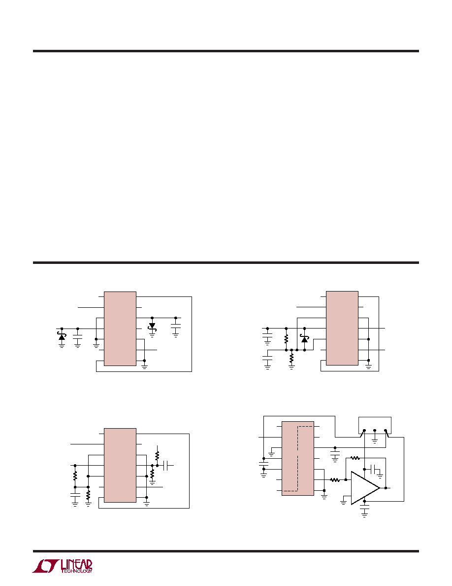
To avoid latchup when the power supplies
exhibit high turn-on transients, a 1N5817 Schottky diode
should be added from the V
+
and V
pins to ground
(Figure 1).
INV A, R(h, I) (Pins 7, 14): A very short connection
between Pin 14 and Pin 7 is recommended. This connec-
tion should be preferably done under the IC package. In a
U
U
U
PI FU CTIO S
breadboard, use a one inch, or less, shielded coaxial cable;
the shield should be grounded. In a PC board, use a one
inch trace or less; surround the trace by a ground plane.
NC (Pins 8, 10): The "no connection" pins preferably
should be grounded.
f
CLK
(Pin 11): For ±5V supplies the logic threshold level is
1.4V. For ±8V and 0V to 5V supplies the logic threshold
levels are 2.2V and 3V respectively. The logic threshold
levels vary ±100mV over the full military temperature
range. The recommended duty cycle of the input clock is
50% although for clock frequencies below 500kHz the
clock "on" time can be as low as 200ns. The maximum
clock frequency for ±5V supplies is 4MHz. For ±7V sup-
plies and above, the maximum clock frequency is 5MHz.
Do not allow the clock levels to exceed the power supplies.
For clock level shifting (see Figure 3).
Figure 1. Using Schottky Diodes to Protect
the IC from Power Supply Spikes
Figure 2. Single Supply Operation. If Fast Power Up
or Down Transients are Expected, Use a 1N5817
Schottky Diode Between Pin 4 and Pin 5.
Figure 3. Level Shifting the Input T
2
L Clock
for Single Supply Operation, V+ >6V.
Figure 4. Buffering the Filter Output. The Buffer Op Amp
Should Not Share the LTC1064-1 Power Lines.
LTC1064-1
1
2
3
4
5
6
7
14
13
12
11
10
9
8
0.1µF
0.1µF
0.1µF
0.1µF
V
OUT
+
V
V
+
POWER SOURCE
10k
10k
1064 F04
RECOMMENDED OP AMPS:
LT1022, LT318, LT1056
COMP2*
V
f
CLK
NC
V
OUT
NC
INV C
V
IN
AGND
V
+
AGND
COMP1*
R(h, I)
INV A
V
IN
LTC1064-1
1
2
3
4
5
6
7
14
13
12
11
10
9
8
V
+
1064 F03
0.1µF
5k
2.2k
5k
5k 1
µF
T
2
L
LEVEL
V
+
R(h, I)
COMP2*
V
f
CLK
NC
V
OUT
NC
INV C
V
IN
AGND
V
+
AGND
COMP1*
INV A
V
OUT
V
IN
LTC1064-1
1
2
3
4
5
6
7
14
13
12
11
10
9
8
V
+
V
1064 F01
0.1µF
0.1µF
1N5817
1N5817
R(h, I)
COMP2*
V
f
CLK
NC
V
OUT
NC
INV C
V
IN
AGND
V
+
AGND
COMP1*
INV A
V
OUT
V
IN
LTC1064-1
1
2
3
4
5
6
7
14
13
12
11
10
9
8
V
+
= 15V
0V TO 10V
1064 F02
0.1µF
0.1µF
5k
5k
V
+
/2
R(h, I)
COMP2*
V
f
CLK
NC
V
OUT
NC
INV C
V
IN
AGND
V
+
AGND
COMP1*
INV A
V
OUT
V
IN
TYPICAL APPLICATIO S
U
(Pin Numbers Refer to the 14-Pin Package)