6554f
LT6554
1
6554f
APPLICATIO S
U
DESCRIPTIO
U
FEATURES
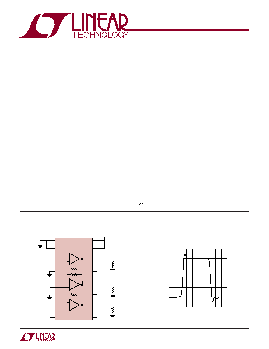
TYPICAL APPLICATIO
U
15
2
5V
16
1
5V
5V
+
14
480
+
12
480
+
10
9
5V
11
5V
13
8
7
6
5
4
3
480
R
IN
G
IN
B
IN
1k
1k
1k
LT6554
6554 TA01a
The LT
®
6554 is a high-speed triple video buffer with an
internally fixed gain of 1. The individual buffers are opti-
mized for performance with a 1k load and feature a
2V
PP
full signal bandwidth of 400MHz, making them ideal
for driving very high-resolution video signals. Separate
power supply pins for each amplifier boost channel sepa-
ration to 90dB, allowing the LT6554 to excel in many high-
speed applications.
While the performance of the LT6554 is optimized for dual
supply operation, it can also be used on a single supply as
low as 4.5V. Using dual 5V supplies, each amplifier draws
only 8mA. When disabled, the amplifiers draw less than
100µA and the outputs become high impedance. Further-
more, the amplifiers are capable of turning on in less than
50ns, making them suitable for multiplexing and portable
applications.
The LT6554 is manufactured on Linear Technology's
proprietary low voltage complementary bipolar process
and is available in the 16-lead SSOP package that fits in the
same PCB area as an SO-8 package.
RGB Buffers
A/D Drivers
LCD Projectors
, LTC and LT are registered trademarks of Linear Technology Corporation.
650MHz 3dB Small Signal Bandwidth
400MHz 3dB 2V
P-P
Large Signal Bandwidth
100MHz ±0.1dB Bandwidth
High Slew Rate: 2500V/µs
Fixed Gain of 1 Requires No External Resistors
90dB Channel Separation at 10MHz
60dB Channel Separation at 100MHz
96dBc 2nd Harmonic Distortion at 10MHz, 2V
P-P
82dBc 3rd Harmonic Distortion at 10MHz, 2V
P-P
Low Supply Current: 8mA per Amplifier
6ns 0.1% Settling Time for 2V Step
TTL Compatible Enable: I
SS
100µA when Disabled
Differential Gain of 0.022%, Differential
Phase of 0.006°
Wide Supply Range: ±2.25V (4.5V) to ±6V (12V)
Available in 16-Lead SSOP Package
650MHz Gain of 1
Triple Video Buffer
Triple Video Buffer and A/D Driver
Large Signal Transient Response
TIME (ns)
OUTPUT (V)
1.5
1.0
0.5
0
0.5
1.0
1.5
4
8
12
16
6554 TA01b
20
2
0
6
10
14
18
V
OUT
= 2V
PP
V
S
= ±5V
R
L
= 1k
T
A
= 25°C
LT6554
2
6554f
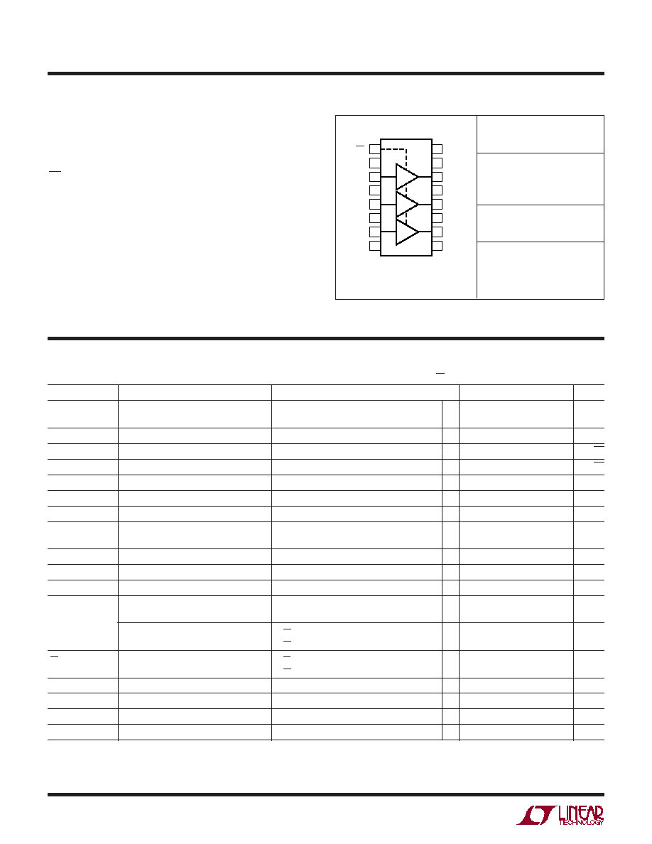
1
2
3
4
5
6
7
8
TOP VIEW
GN PACKAGE
16-LEAD PLASTIC SSOP
16
15
14
13
12
11
10
9
EN
DGND
INR
AGND
ING
AGND
INB
V
V
+
V
+
OUTR
V
OUTG
V
+
OUTB
V
G = +1
G = +1
G = +1
Total Supply Voltage (V
+
to V
) ............................ 13.2V
Input Current (Note 2) ........................................ ±10mA
Output Current (Continuous) ............................. ±70mA
EN to DGND Voltage (Note 2) ................................. 5.5V
Output Short-Circuit Duration (Note 3) ............ Indefinite
Operating Temperature Range (Note 4) ... 40°C to 85°C
Specified Temperature Range (Note 5) .... 40°C to 85°C
Storage Temperature Range .................. 65°C to 150°C
Junction Temperature ........................................... 150°C
Lead Temperature (Soldering, 10 sec).................. 300°C
ORDER PART
NUMBER
GN PART
MARKING
T
JMAX
= 150°C,
JA
= 135°C/W
Consult LTC Marketing for parts specified with wider operating temperature ranges.
6554
6554I
LT6554CGN
LT6554IGN
ABSOLUTE AXI U
RATI GS
W
W
W
U
PACKAGE/ORDER I FOR ATIO
U
U
W
(Note 1)
ELECTRICAL CHARACTERISTICS
The
denotes the specifications which apply over the full operating
temperature range, otherwise specifications are at T
A
= 25°C. V
S
= ±5V, R
L
= 1k, C
L
= 1.5pF, V
EN
= 0.4V, V
AGND
, V
DGND
= 0V.
SYMBOL
PARAMETER
CONDITIONS
MIN
TYP
MAX
UNITS
V
OS
Offset Voltage
V
IN
= 0V, V
OS
= V
OUT
11
±35
mV
±70
mV
I
IN
Input Current
17
±50
µA
e
n
Output Noise Voltage
f = 100kHz
20
nVHz
i
n
Input Noise Current
f = 100kHz
3.5
pAHz
R
IN
Input Resistance
V
IN
= ±1V
150
400
k
C
IN
Input Capacitance
f = 100kHz
1
pF
PSRR
Power Supply Rejection Ratio
V
S
(Total) = 4.5V to 12V (Note 6)
51
65
dB
I
PSRR
Input Current Power Supply
V
S
(Total) = 4.5V to 12V (Note 6)
1
±5
µA/V
Rejection
A
V
ERR
Gain Error
V
OUT
= ±2V
2.5
0.6
0
%
A
V
MATCH
Gain Matching
Any One Channel to Another
±0.03
%
V
OUT
Maximum Output Voltage Swing
±3.75
±3.85
V
I
S
Supply Current, Per Amplifier
8
10
mA
13
mA
Supply Current, Disabled, Total
V
EN
= 4V
22
100
µA
V
EN
= Open
0.5
100
µA
I
EN
Enable Pin Current
V
EN
= 0.4V
200
95
µA
V
EN
= V
+
0.5
50
µA
I
SC
Output Short-Circuit Current
R
L
= 0, V
IN
= ±1V
±50
±105
mA
SR
Slew Rate
4V
P-P
Output Step (Note 9)
1700
2500
V/µs
3dB BW
Small Signal 3dB Bandwidth
V
OUT
= 200mV
P-P
650
MHz
0.1dB BW
Gain Flatness ±0.1dB Bandwidth
V
OUT
= 200mV
P-P
100
MHz
LT6554
3
6554f
LSBW
Large Signal Bandwidth
V
OUT
= 2V
P-P
(Note 7)
270
400
MHz
V
OUT
= 4V
P-P
(Note 7)
200
MHz
All-Hostile Crosstalk
f = 10MHz, V
OUT
= 2V
P-P
90
dB
f = 100MHz, V
OUT
= 2V
P-P
60
dB
t
S
Settling Time
0.1% of V
FINAL
, V
STEP
= 2V
6
ns
t
R
,
t
F
Small-Signal Rise and Fall Time
10% to 90%, V
OUT
= 200mV
P-P
550
ps
dG
Differential Gain
(Note 8)
0.022
%
dP
Differential Phase
(Note 8)
0.006
Deg
HD2
2nd Harmonic Distortion
f = 10MHz, V
OUT
= 2V
P-P
96
dBc
HD3
3rd Harmonic Distortion
f = 10MHz, V
OUT
= 2V
P-P
82
dBc
ELECTRICAL CHARACTERISTICS
The
denotes the specifications which apply over the full operating
temperature range, otherwise specifications are at T
A
= 25°C. V
S
= ±5V, R
L
= 1k, C
L
= 1.5pF, V
EN
= 0.4V, V
AGND
, V
DGND
= 0V.
SYMBOL
PARAMETER
CONDITIONS
MIN
TYP
MAX
UNITS
Note 1: Absolute Maximum Ratings are those values beyond which the life
of a device may be impaired.
Note 2: This parameter is guaranteed to meet specified performance
through design and characterization. It is not production tested.
Note 3: As long as output current and junction temperature are kept below
the Absolute Maximum Ratings, no damage to the part will occur.
Depending on the supply voltage, a heat sink may be required.
Note 4: The LT6554C is guaranteed functional over the operating
temperature range of 40°C to 85°C.
Note 5: The LT6554C is guaranteed to meet specified performance from
0°C to 70°C. The LT6554C is designed, characterized and expected to
meet specified performance from 40°C and 85°C but is not tested or QA
sampled at these temperatures. The LT6554I is guaranteed to meet
specified performance from 40°C to 85°C.
Note 6: The two supply voltage settings for power supply rejection are
shifted from the typical ±V
S
points for ease of testing. The first
measurement is taken at V
+
= 3V, V
= 1.5V to provide the required 3V
headroom for the enable circuitry to function with EN, DGND, AGND and
all inputs connected to 0V. The second measurement is taken at V
+
= 8V,
V
= 4V.
Note 7: Large signal bandwidth is calculated from the slew rate:
LSBW = SR/( · V
P-P
)
Note 8: Differential gain and phase are measured using a Tektronix
TSG120YC/NTSC signal generator and a Tektronix 1780R video
measurement set. The resolution of this equipment is better than 0.05%
and 0.05°. Nine identical amplifier stages were cascaded giving an
effective resolution of better than 0.0056% and 0.0056°.
Note 9: Slew rate is 100% production tested on the G channel. Slew rate
of the R and B channels is guaranteed through design and
characterization.
LT6554
4
6554f
INPUT VOLTAGE (V)
2.5
INPUT BIAS CURRENT (
µ
A)
20
0
1.5
6554 G05
40
60
1.5
0.5
0.5
2.5
20
V
S
= ±5V
T
A
= 55°C
T
A
= 25°C
T
A
= 125°C
EN PIN VOLTAGE (V)
0
EN PIN CURRENT (
µ
A)
0
20
40
60
80
100
120
140
6554 G06
2
5
1
3
4
V
S
= ±5V
V
DGND
= 0V
T
A
= 55°C
T
A
= 25°C
T
A
= 125°C
TEMPERATURE (°C)
55
SUPPLY CURRENT (mA)
15
25
45
125
6554 G01
35
5
65
85 105
12
10
8
6
4
2
0
TOTAL SUPPLY VOLTAGE (V)
0
4
6554 G02
1
2
3
5
6
7
8
9 10 11 12
SUPPLY CURRENT (mA)
12
10
8
6
4
2
0
EN PIN VOLTAGE (V)
SUPPLY CURRENT (mA)
6554 G03
12
10
8
6
4
2
0
0
1.0
2.0
2.5
0.5
1.5
3.0
3.5
4.0
V
S
= ±5V
R
L
=
V
IN
= 0V
V
S
= ±5V
V
DGND
= 0V
V
IN
= 0V
V
EN
= 0V
V
EN
= 0.4V
V
= V
+
V
EN
, V
DGND
, V
IN
= 0V
T
A
= 25°C
T
A
= 55°C
T
A
= 25°C
T
A
= 125°C
SOURCE CURRENT (mA)
0
OUTPUT VOLTAGE (V)
5
4
3
2
1
0
40
6554 G08
10
20 30
100
50
60 70 80 90
V
S
= ±5V
V
IN
= 4V
T
A
= 125°C
T
A
= 55°C
T
A
= 25°C
0
40
10
20 30
100
50
60 70 80 90
SINK CURRENT (mA)
OUTPUT VOLTAGE (V)
0
1
2
3
4
5
6554 G09
V
S
= ±5V
V
IN
= 4V
T
A
= 125°C
T
A
= 55°C
T
A
= 25°C
6554 G07
6554 G04
INPUT VOLTAGE (V)
4.5
OUTPUT VOLTAGE (V)
5
4
3
2
1
0
1
2
3
4
5
2.5
0.5 0.5
4.5
3.5
1.5
1.5 2.5 3.5
T
A
= 25°C
T
A
= 55°C
V
S
= ±5V
R
L
= 1k
T
A
= 125°C
TEMPERATURE (°C)
55
OFFSET VOLTAGE (mV)
15
25
45
125
35
5
65
85 105
15.0
12.5
10.0
7.5
5.0
2.5
0
2.5
5.0
V
S
= ±5V
V
IN
= 0V
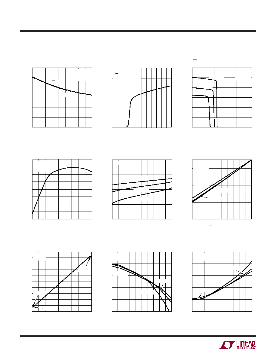
TYPICAL PART
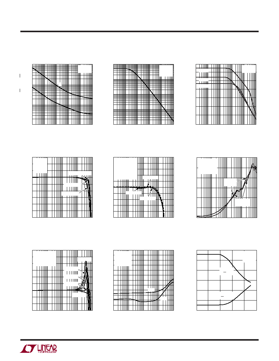
TYPICAL PERFOR A CE CHARACTERISTICS
U
W
Output Voltage Swing vs I
LOAD
(Output High)
Output Voltage Swing vs I
LOAD
(Output Low)
Input Bias Current vs
Input Voltage
Output Voltage vs Input Voltage
EN Pin Current vs EN Pin Voltage
Offset Voltage vs Temperature
Supply Current per Amplifier vs
Temperature
Supply Current per Amplifier vs
Supply Voltage
Supply Current per Amplifier vs
EN Pin Voltage
LT6554
5
6554f
6554 G11
6554 G10
FREQUENCY (kHz)
INPUT NOISE (nV/
Hz OR pA/
Hz)
0.001
0.01
1
10
100
0.1
1000
100
10
1
6554 G12
FREQUENCY (MHz)
REJECTION RATIO (dB)
0.001
0.01
1
10
100
0.1
FREQUENCY (MHz)
INPUT IMPEDANCE (k
)
0.01
0.1
10
100
1000
1
1000
100
10
1
0.1
70
60
50
40
30
20
10
0
V
S
= ±5V
T
A
= 25°C
i
n
PSRR
+PSRR
±PSRR
V
S
= ±5V
T
A
= 25°C
V
S
= ±5V
V
IN
= 0V
T
A
= 25°C
e
n
6554 G13
6554 G14
6554 G16
6554 G17
6554 G18
FREQUENCY (MHz)
0.1
AMPLITUDE (dB)
0
20
40
60
80
100
120
1
10
100
1000
6554 G15
V
S
= ±5V
V
OUT
= 2V
P-P
R
L
= 1k
T
A
= 25°C
ALL-
HOSTILE
WORST
ADJACENT
FREQUENCY (MHz)
0.1
AMPLITUDE (dB)
10
1000
3
2
1
0
1
2
3
4
5
6
1
100
V
OUT
= 200mV
P-P
V
OUT
= 4V
P-P
V
OUT
= 2V
P-P
V
S
= ±5V
R
L
= 1k
C
L
= 1.5pF
T
A
= 25°C
FREQUENCY (MHz)
AMPLITUDE (dB)
0.5
0.4
0.3
0.2
0.1
0
0.1
0.2
0.3
0.4
0.5
0.1
10
100
1000
1
G-CHANNEL
B-CHANNEL
R-CHANNEL
V
S
= ±5V
V
OUT
= 200mV
P-P
R
L
= 1k
C
L
= 1.5pF
T
A
= 25°C
TYPICAL PART
FREQUENCY (MHz)
0.1
AMPLITUDE (dB)
10
1000
12
10
8
6
4
2
0
2
4
6
1
100
V
S
= ±5V
V
OUT
= 200mV
P-P
R
L
= 1k
T
A
= 25°C
C
L
= 12pF
C
L
= 9pF
C
L
= 6.8pF
C
L
= 3.3pF
C
L
= 1.5pF
DISTORTION (dBc)
0
10
20
30
40
50
60
70
80
90
100
110
120
FREQUENCY (MHz)
0.01
1
10
100
0.1
HD2
HD3
V
S
= ±5V
V
OUT
= 2V
P-P
R
L
= 1k
T
A
= 25°C
FREQUENCY (MHz)
0.01
OUTPUT IMPEDANCE (
)
100000
10000
1000
100
10
1
0.1
0.1
1
10
100
1000
V
S
= ±5V
R
L
= 1k
T
A
= 25°C
DISABLED
V
EN
= 4V
ENABLED
V
EN
= 0.4V
TYPICAL PERFOR A CE CHARACTERISTICS
U
W
Frequency Response
Gain Flatness vs Frequency
Crosstalk vs Frequency
Frequency Response with
Capacitive Loads
Harmonic Distortion vs Frequency
Output Impedance vs Frequency
Input Noise Spectral Density
Input Impedance vs Frequency
PSRR vs Frequency