Äîêóìåíòàöèÿ è îïèñàíèÿ www.docs.chipfind.ru
1
LT3466
3466f
Dual Full Function White LED
Step-Up Converter with
Built-In Schottky Diodes
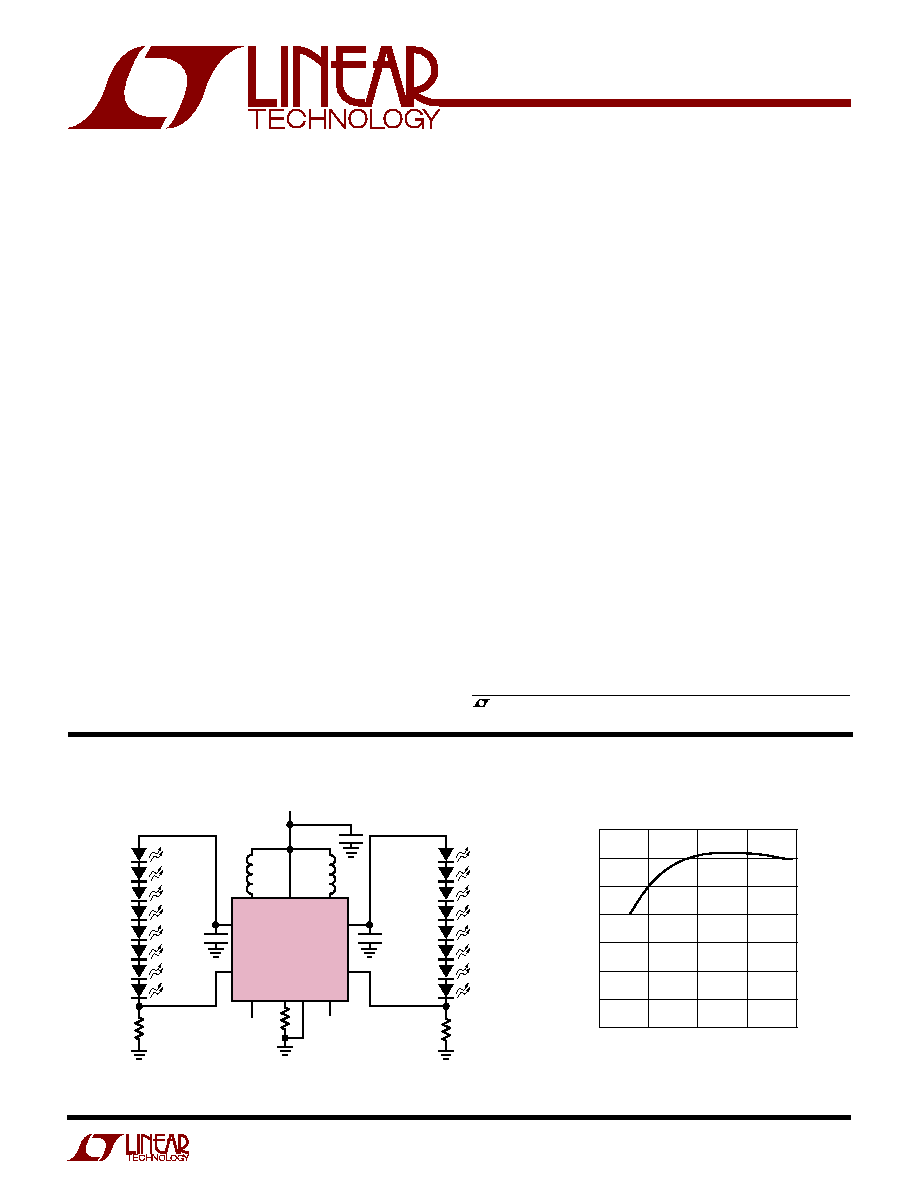
Figure 1. Li-Ion Powered Driver for 8/8 White LEDs
s
Drives Up to 20 White LEDs (10 in Series
per Converter) from a 3.6V Supply
s
Two Independent Step-Up Converters Capable of
Driving Asymmetric LED Strings
s
Independent Dimming and Shutdown Control
of the Two LED Strings
s
Internal Schottky Diodes
s
Internal Soft-Start Eliminates Inrush Current
s
Open LED Protection (42V Max V
OUT
)
s
Fixed Frequency Operation Up to 2MHz
s
81% Efficiency Driving 16 White LEDs at 15mA
(Eight per Driver) from a 3.6V Supply
s
Wide Input Voltage Range: 2.7V to 24V
s
Tiny (3mm
×
3mm) 10-Lead DFN Package
, LTC and LT are registered trademarks of Linear Technology Corporation.
s
Main/Sub Displays
s
Digital Cameras, Sub-Notebook PCs
s
PDAs, Handheld Computers
s
Automotive
LT
®
3466 is a dual full function step-up DC/DC converter
specifically designed to drive up to 20 White LEDs (10 in
series per converter) with a constant current. Series
connection of the LEDs provides identical LED currents
resulting in uniform brightness and eliminating the need
for ballast resistors and expensive factory calibration.
The two independent converters are capable of driving
asymmetric LED strings. The dimming of the two LED
strings can also be controlled independently. The LT3466
is ideal for providing backlight for main and sub-displays
in cell phones and other handheld devices.
The LT3466 operating frequency can be set with an
external resistor over a 200kHz to 2MHz range. A low
200mV feedback voltage minimizes power loss in the
current setting resistor for better efficiency. Additional
features include output voltage limiting when LEDs are
disconnected and internal soft-start.
The LT3466 is available in a low profile, small footprint
(3mm
×
3mm
×
0.75mm) DFN package.
CTRL1
GND CTRL2
R
T
SW1
SW2
V
IN
3V TO 5V
47
µ
H
1
µ
F
2.2
µ
F
2.2
µ
F
LED1
LED2
47
µ
H
LT3466
SHUTDOWN
AND DIMMING
CONTROL 2
SHUTDOWN
AND DIMMING
CONTROL 1
V
OUT1
FB1
10
10
3466 F01a
V
OUT2
FB2
63.4k
Conversion Efficiency
LED CURRENT (mA)
0
EFFICIENCY (%)
70
75
20
3466 F01b
60
50
65
55
5
10
15
85
V
IN
= 3.6V
8/8 LEDs
80
DESCRIPTIO
U
FEATURES
APPLICATIO S
U
TYPICAL APPLICATIO
U
2
LT3466
3466f
(Note 1)
Input Voltage (V
IN
) ................................................... 24V
SW1, SW2 Voltages ................................................ 44V
V
OUT1
, V
OUT2
Voltages ............................................. 44V
CTRL1, CTRL2 Voltages ........................................... 24V
FB1, FB2, R
T
Voltages ................................................ 2V
Operating Temperature Range ................ 40
°
C to 85
°
C
Storage Temperature Range .................. 65
°
C to 125
°
C
Junction Temperature .......................................... 125
°
C
ABSOLUTE AXI U RATI GS
W
W
W
U
PACKAGE/ORDER I FOR ATIO
U
U
W
T
JMAX
= 125
°
C,
JA
= 43
°
C/W,
JC
= 2.96
°
C/W
EXPOSED PAD (PIN 11) IS GND
MUST BE SOLDERED TO PCB
ORDER PART
NUMBER
DD PART MARKING
LBBH
LT3466EDD
Consult LTC Marketing for parts specified with wider operating temperature ranges.
ELECTRICAL CHARACTERISTICS
The
q
denotes specifications that apply over the full operating temperature
range, otherwise specifications are at T
A
= 25
°
C. V
IN
= 3V, V
CTRL1
= 3V, V
CTRL2
= 3V, unless otherwise specified.
PARAMETER
CONDITIONS
MIN
TYP
MAX
UNITS
Minimum Operating Voltage
2.7
V
Maximum Operating Voltage
24
V
FB1 Voltage
q
192
200
208
mV
FB2 Voltage
q
192
200
208
mV
FB1 Pin Bias Current
V
FB1
= 0.2V (Note 3)
10
50
nA
FB2 Pin Bias Current
V
FB2
= 0.2V (Note 3)
10
50
nA
Quiescent Current
V
FB1
= V
FB2
= 0.3V
5
6
mA
CTRL1 = CTRL2 = 0V
16
25
µ
A
Switching Frequency
R
T
= 48.7k
0.8
1
1.2
MHz
Oscillator Frequency Range
200
2000
kHz
Nominal R
T
Pin Voltage
R
T
= 48.7k
0.54
V
Maximum Duty Cycle
R
T
= 48.7k
q
90
96
%
R
T
= 20.5k
92
%
R
T
= 267k
99
%
Converter 1 Current Limit
q
320
400
mA
Converter 2 Current Limit
q
320
400
mA
Converter 1 V
CESAT
I
SW1
= 300mA
360
mV
Converter 2 V
CESAT
I
SW2
= 300mA
360
mV
Switch 1 Leakage Current
V
SW1
= 10V
0.01
5
µ
A
Switch 2 Leakage Current
V
SW2
= 10V
0.01
5
µ
A
CTRL1 Voltage for Full LED Current
1.8
V
CTRL2 Voltage for Full LED Current
1.8
V
CTRL1 and CTRL2 Voltage to Shut Down Chip
50
mV
CTRL1, CTRL2 Pin Bias Current
V
CTRL1
= V
CTRL2
= 1V
q
8
10
12
µ
A
V
OUT1
Overvoltage Threshold
42
V
V
OUT2
Overvoltage Threshold
42
V
TOP VIEW
11
DD PACKAGE
10-LEAD (3mm
×
3mm) PLASTIC DFN
10
9
6
7
8
4
5
3
2
1
FB1
CTRL1
R
T
CTRL2
FB2
V
OUT1
SW1
V
IN
SW2
V
OUT2
3
LT3466
3466f
ELECTRICAL CHARACTERISTICS
The
q
denotes specifications that apply over the full operating temperature
range, otherwise specifications are at T
A
= 25
°
C. V
IN
= 3V, V
CTRL1
= 3V, V
CTRL2
= 3V, unless otherwise specified.
PARAMETER
CONDITIONS
MIN
TYP
MAX
UNITS
Schottky 1 Forward Drop
I
SCHOTTKY1
= 300mA
0.85
V
Schottky 2 Forward Drop
I
SCHOTTKY2
= 300mA
0.85
V
Schottky 1 Reverse Leakage
V
OUT1
= 20V
5
µ
A
Schottky 2 Reverse Leakage
V
OUT2
= 20V
5
µ
A
Soft-Start Time (Switcher 1)
600
µ
s
Soft-Start Time (Switcher 2)
600
µ
s
Note 1: Absolute Maximum Ratings are those values beyond which the life
of a device may be impaired.
Note 2: The LTC3466E is guaranteed to meet specified performance from
0
°
C to 70
°
C. Specifications over the 40
°
C to 85
°
C operating range are
assured by design, characterization and correlation with statistical process
controls.
Note 3: Current flows out of the pin.
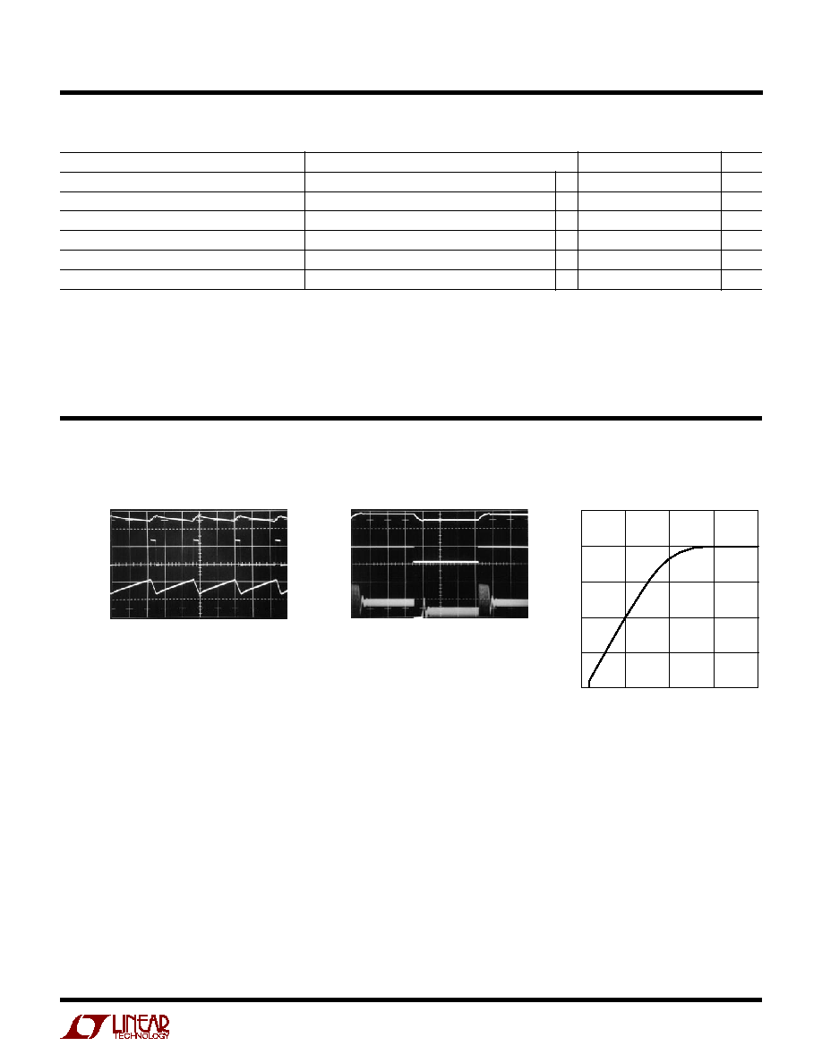
TYPICAL PERFOR A CE CHARACTERISTICS
U
W
Switching Waveforms
Transient Response
V
FB1,2
vs V
CTRL1,2
V
OUT1
50mV/DIV
V
SW1
20V/DIV
I
L1
100mA/DIV
V
IN
= 3.6V
0.5
µ
s/DIV
3466 G01
CIRCUIT OF FIGURE 1
V
OUT1
0.5V/DIV
V
CTRL1
2V/DIV
I
L1
200mA/DIV
V
IN
= 3.6V
5
µ
s/DIV
3466 G02
I
LED1
= 20mA TO 10mA
CIRCUIT OF FIGURE 1
CONTROL VOLTAGE (V)
0
FEEDBACK VOLTAGE (mV)
100
150
2
3466 G03
50
0
0.5
1
1.5
250
200
V
IN
= 3V
T
A
= 25
°
C
4
LT3466
3466f
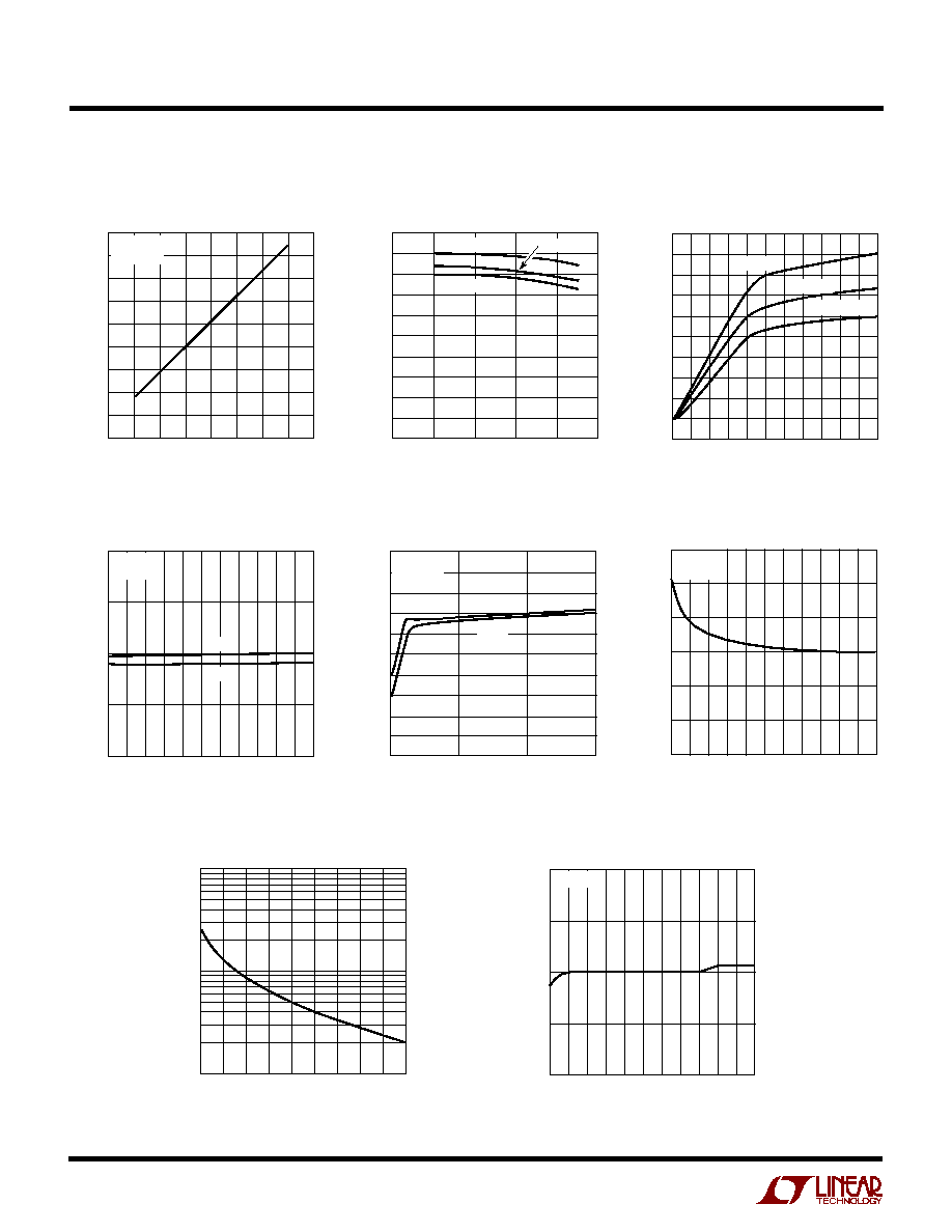
TYPICAL PERFOR A CE CHARACTERISTICS
U
W
Switch Saturation Voltage (V
CESAT
)
Switch Current Limit vs Duty Cycle
Shutdown Quiescent Current
(CTRL1 = CTRL2 = 0V)
Open-Circuit Output Clamp
Voltage
R
T
vs Oscillator Frequency
SWITCH CURRENT (mA)
0
SWITCH SATURATION VOLTAGE (mV)
250
300
350
400
3466 G04
200
150
0
100
200
300
50
150
250
350
100
50
450
400
T
A
= 25
°
C
V
CE1
, V
CE2
DUTY CYCLE (%)
0
CURRENT LIMIT (mA)
300
400
80
3466 G05
200
100
250
350
450
500
150
50
0
20
40
60
100
T
A
= 50
°
C
T
A
= 85
°
C
T
A
= 25
°
C
V
IN
(V)
4
SHUTDOWN CURRENT (
µ
A)
60
80
100
20
3466 G06
40
20
50
70
90
30
10
0
8
12
16
6
2
22
10
14
18
24
T
A
= 50
°
C
T
A
= 100
°
C
T
A
= 25
°
C
V
IN
(V)
2
OUTPUT CLAMP VOLTAGE (V)
42
43
18
3466 G07
41
40
6
10 12
24
44
14
4
8
20 22
16
T
A
= 25
°
C
R
T
= 48.7k
V
OUT2
V
OUT1
TEMPERATURE (
°
C)
50
35
OUTPUT CLAMP VOLTAGE (V)
37
38
39
40
41
42
0
50
3466 G08
43
44
45
36
100
V
IN
= 3.6V
R
T
= 48.7k
V
OUT2
V
OUT1
V
IN
(V)
0
INPUT CURRENT (mA)
4
8
12
2
6
10
6
10
14
18
3466 G09
24
4
2
8
12
16
20 22
T
A
= 25
°
C
R
T
= 48.7k
Open-Circuit Output Clamp
Voltage
Input Current with Output 1 and
Output 2 Open Circuit
OSCILLATOR FREQUENCY (kHz)
R
T
(k
)
1000
3466 G10
10
100
600
1800
1400
1000
200
Oscillator Frequency vs V
IN
V
IN
(V)
2
OSCILLATOR FREQUENCY (kHz)
1000
1100
18
3466 G11
900
800
6
10 12
24
1200
14
4
8
20 22
16
R
T
= 48.7k
5
LT3466
3466f
TYPICAL PERFOR A CE CHARACTERISTICS
U
W
Schottky Forward Voltage Drop
Schottky Leakage Current
Quiescent Current
(CTRL1 = CTRL2 = 3V)
V
IN
(V)
0
0
QUIESCENT CURRENT (mA)
1
2
3
4
6
4
8
12
16
3466 G13
20
24
5
T
A
= 25
°
C
SCHOTTKY FORWARD DROP (mV)
0
SCHOTTKY FORWARD CURRENT (mA)
150
200
250
600
1000
3466 G14
100
50
0
200
400
800
300
350
400
T
A
= 25
°
C
TEMPERATURE (
°
C)
50
0
SCHOTTKY LEAKAGE CURRENT (
µ
A)
1
2
3
4
6
0
50
3466 G15
100
V
R
= 40V
5
V
R
= 20V
Oscillator Frequency
vs Temperature
TEMPERATURE (
°
C)
50
OSCILLATOR FREQUENCY (kHz)
1250
1500
1750
3466 G12
1000
750
500
0
50
2000
2250
2500
100
V
IN
= 3.6V
R
T
= 20.5k
R
T
= 48.7k