Äîêóìåíòàöèÿ è îïèñàíèÿ www.docs.chipfind.ru
LT3464
1
3464i
s
Tiny Solution Size
s
Low Quiescent Current
· 25
µ
A in Active Mode
· 0.5
µ
A in Shutdown Mode
s
Integrated Schottky Diode
s
Integrated PNP Output Disconnect with
Short-Circuit Protection
s
Internal Reference Override Pin
s
16V at 8mA from 3.6V Input
s
12V at 20mA from 5V Input
s
Low V
CE(SAT)
Switch: 190mV at 80mA
s
Input Range: 2.3V to 10V
s
High Output Voltage: Up to 34V
s
Low Profile (1mm) ThinSOT Package
APPLICATIO S
U
FEATURES
DESCRIPTIO
U
TYPICAL APPLICATIO
U
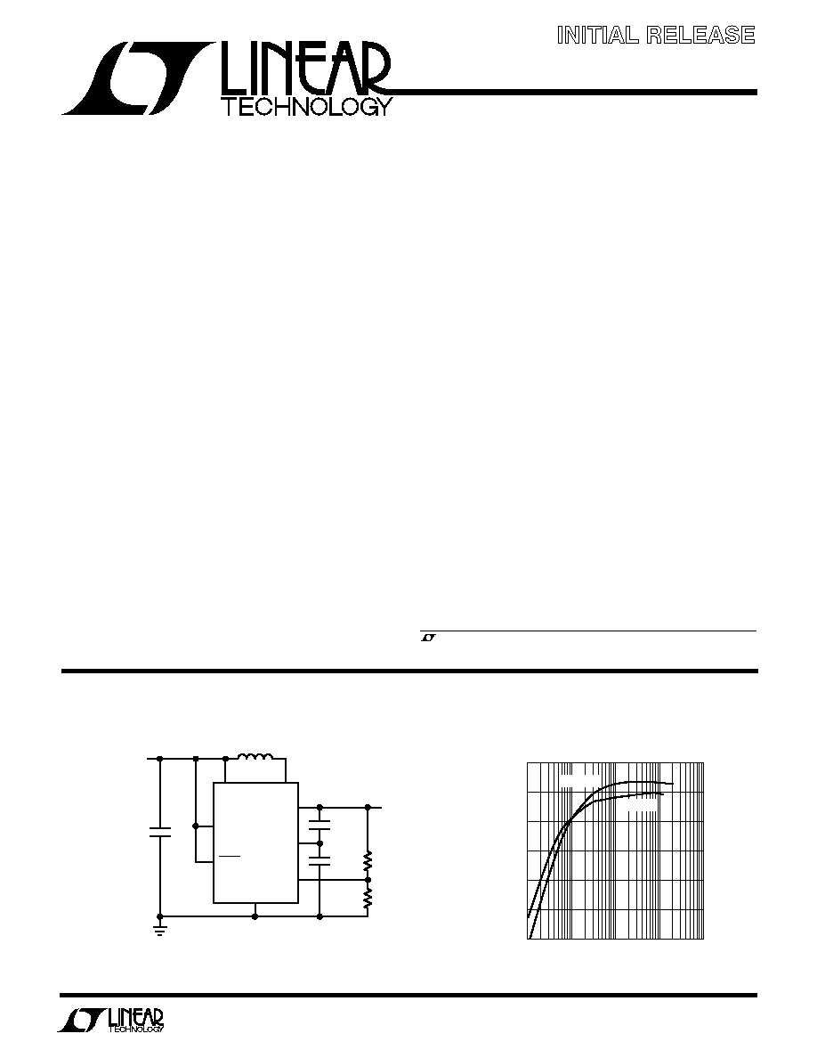
Micropower Boost
Converter with Integrated Schottky
and Output Disconnect in ThinSOT
January 2003
The LT
®
3464 is a micropower step-up DC/DC converter
with integrated Schottky diode and output disconnect
packaged in an 8-lead low profile (1mm) ThinSOT
TM
. The
small package size, high level of integration, and the use
of tiny SMT components yield a solution size of less than
40mm
2
. The LT3464 has a typical current limit of 115mA
as well as fast switching speed to allow the use of a chip
inductor and small ceramic capacitors. The internal PNP
disconnects the output load from the input during shut-
down, and also provides output short-circuit protection.
An auxiliary reference input allows the user to override the
internal 1.25V feedback reference with any lower value,
allowing full control of the output voltage during opera-
tion. This device features a low 25
µ
A quiescent current,
which is further reduced to less than 1
µ
A in shutdown. A
current limited fixed off-time control scheme conserves
operating current, resulting in high efficiency over a broad
range of operating current. The rugged 36V switch and
output disconnect circuitry allow outputs up to 34V to be
easily generated in a simple boost topology.
, LTC and LT are registered trademarks of Linear Technology Corporation.
s
LCD Bias
s
Handheld Computers
s
Battery Backup
s
Digital Cameras
s
Cellular Phones
CTRL
SHDN
V
IN
V
IN
2.3V TO 10V
V
OUT
16V
SW
GND
OUT
CAP
FB
LT3464
L1
22
µ
H
C1
1
µ
F
C3
0.22
µ
F
C2
0.33
µ
F
3.48M
294k
1
8
7
6
3
5
2
4
3464 TA01a
C1: TAIYO YUDEN LMK107 BJ105MA-T
C2: TAIYO YUDEN GMK212 BJ474MG-T
C3: TAIYO YUDEN GMK212 BJ224MG-T
L1: MURATA LQH32CN220K
ThinSOT is a trademark of Linear Technolgy Corporation
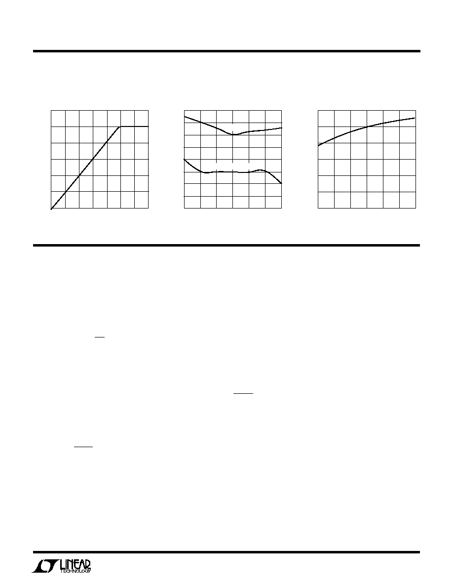
Efficiency
Final Electrical Specifications
Information furnished by Linear Technology Corporation is believed to be accurate and reliable.
However, no responsibility is assumed for its use. Linear Technology Corporation makes no represen-
tation that the interconnection of its circuits as described herein will not infringe on existing patent rights.
LOAD CURRENT (mA)
EFFICIENCY (%)
90
80
70
60
50
40
30
0.01
1
10
100
3634 TA01b
0.1
V
IN
= 8.4V
V
IN
= 4.2V
LT3464
2
3464i
V
IN
, SHDN, CTRL Voltage ........................................ 10V
OUT, CAP Voltage .................................................... 36V
SW Voltage .............................................................. 36V
FB Voltage ................................................................. 6V
Maximum Junction Temperature .......................... 125
°
C
Operating Temperature Range (Note 2) .. 40
°
C to 85
°
C
Storage Temperature Range ..................65
°
C to 150
°
C
Lead Temperature (Soldering, 10 sec).................. 300
°
C
ORDER PART
NUMBER
T
JMAX
= 125
°
C,
JA
= 140
°
C/W
LT3464ETS8
ABSOLUTE AXI U
RATI GS
W
W
W
U
PACKAGE/ORDER I FOR ATIO
U
U
W
(Note 1)
ELECTRICAL CHARACTERISTICS
The
q
denotes the specifications which apply over the full operating
temperature range, otherwise specifications are at T
A
= 25
°
C. V
IN
= 3.6V, unless otherwise noted. (Note 2)
PARAMETER
CONDITIONS
MIN
TYP
MAX
UNITS
Minimum Input Voltage
2.0
2.3
V
Quiescent Current
Not Switching
25
36
µ
A
V
SHDN
= 0.2V
0.01
0.5
µ
A
FB Comparator Trip Voltage
V
FB
Falling, V
CTRL
= 3.6V
q
1.215
1.250
1.275
V
FB Comparator Hysteresis
10
mV
FB Pin Bias Current
V
FB
= 1.25V, V
CTRL
= 3.6V
q
3
30
nA
FB Voltage Line Regulation
2.3V < V
IN
< 10V
0.05
0.1
%/V
Switch Off Time
V
CAP
-V
IN
= 5V
250
ns
V
CAP
-V
IN
= 0V
1.0
µ
s
Switch Leakage Current
V
SW
= 36V
0.02
1
µ
A
Switch V
CESAT
I
SW
= 80mA
190
300
mV
Switch Current Limit
85
115
140
mA
Schottky Forward Voltage
I
SCHOTTKY
= 110mA
600
750
mV
Schottky Reverse Leakage
V
CAP-SW
= 36V
1
10
µ
A
PNP Disconnect V
CAP-OUT
I
OUT
= 200
µ
A
100
mV
I
OUT
= 10mA
190
mV
PNP Disconnect Q Current
I
OUT
= 0, V
CAP
= 36V (Note 3)
1.5
5
µ
A
PNP Disconnect Leakage
SHDN = 0.2, V
CAP
= 10V, V
OUT
= 0V
0.1
5
µ
A
PNP Disconnect Current Limit
V
CAP
= 10V, V
OUT
= 0V
25
45
75
mA
SHDN Pin Current
V
SHDN
= 3.6V
5
10
µ
A
SHDN Input Voltage High
2.3
V
SHDN Input Voltage Low
0.2
V
CTRL Pin Bias Current
V
CTRL
= 0.5V, V
FB
= 1V
q
6
80
nA
CTRL to FB Offset
V
CTRL
= 0.5V (Note 4)
2
7
mV
Consult LTC Marketing for parts specified with wider operating temperature ranges.
Note 1: Absolute Maximum Ratings are those values beyond which the life
of a device may be impaired.
Note 2: The LT3464E is guaranteed to meet performance specifications
from 0
°
C to 70
°
C. Specifications over the 40
°
C to 85
°
C operating
temperature range are assured by design, characterization and correlation
with statistical process controls.
Note 3: Current consumed by Disconnect PNP when there is no load on
the OUT pin.
Note 4: This figure is computed according to ((V
FB
falling + V
FB
rising)/2)
V
CONTROL
.
CTRL 1
FB 2
OUT 3
GND 4
8 SHDN
7 V
IN
6 SW
5 CAP
TOP VIEW
TS8 PACKAGE
8-LEAD PLASTIC SOT-23
TS8 PART MARKING
LTG2
LT3464
3
3464i
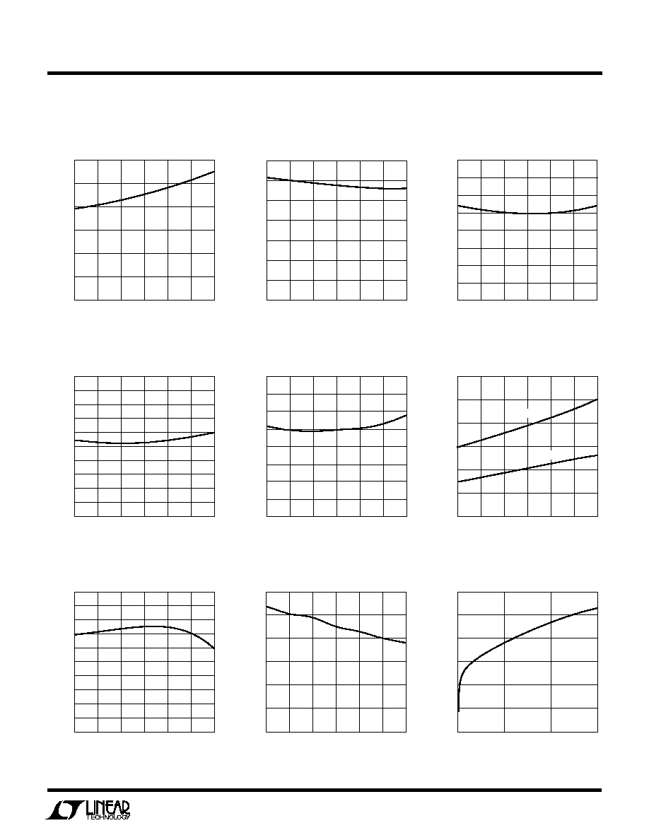
TYPICAL PERFOR A CE CHARACTERISTICS
U
W
Switch Saturation Voltage
I
SW
= 80mA
Switch Current Limit
Switch Off-Time, V
CAP
V
IN
= 5V
Minimum Switch On-Time
Switch Off-Time, V
CAP
V
IN
= 0V
Output Disconnect Voltage Drop
Output Disconnect Quiescent
Current
Output Disconnect Current Limit
Output Disconnect Voltage Drop
SWITCH VOLTAGE (mV)
220
200
180
160
140
120
100
3464 G01
CURRENT LIMIT (mA)
60
50
40
30
20
10
0
COLLECTOR CURRENT (mA)
0
VOLTAGE DROP (mV)
300
250
200
150
100
50
0
10
20
3464 G09
30
VOLTAGE DROP (mV)
300
250
200
150
100
50
0
3464 G06
TEMPERATURE (
°
C)
SWITCH CURRENT (mA)
140
120
100
80
60
40
20
0
3464 G02
50
25
0
25
50
75
100
TEMPERATURE (
°
C)
50
25
0
25
50
75
100
TEMPERATURE (
°
C)
50
25
0
25
50
75
100
TEMPERATURE (
°
C)
50
25
0
25
50
75
100
TEMPERATURE (
°
C)
50
25
0
25
50
75
100
TEMPERATURE (
°
C)
50
25
0
25
50
75
100
SWITCH OFF-TIME (ns)
3464 G03
400
350
300
250
200
150
100
50
0
SWITCH OFF-TIME (
µ
s)
3464 G05
1.3
1.2
1.1
1.0
0.9
0.8
0.7
0.6
0.5
SWITCH ON-TIME (ns)
3464 G04
TEMPERATURE (
°
C)
50
25
0
25
50
75
100
3464 G07
TEMPERATURE (
°
C)
50
25
0
25
50
75
100
3464 G08
100
90
80
70
60
50
40
30
20
10
0
QUIESCENT CURRENT (
µ
A)
2.0
1.8
1.6
1.4
1.2
1.0
0.8
0.6
0.4
0.2
0
I
OUT
= 200
µ
A
I
OUT
= 10mA
LT3464
4
3464i
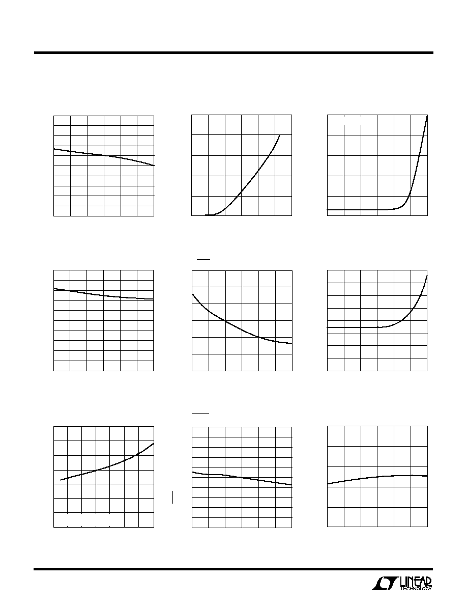
SHUTDOWN PIN CURRENT (
µ
A)
12
10
8
6
4
2
0
3464 G13
TEMPERATURE (
°
C)
50
25
0
25
50
75
100
FB PIN VOLTAGE (V)
1.30
1.28
1.26
1.24
1.22
1.20
3464 G16
TEMPERATURE (
°
C)
50
25
0
25
50
75
100
LEAKAGE CURRENT (
µ
A)
20
16
12
8
4
0
TEMPERATURE (
°
C)
50
25
0
25
50
75
100
SCHOTTKY CURRENT (mA)
250
200
150
100
50
0
3464 G11
FORWARD VOLTAGE (mV)
200
300
400
500
600
700
800
TEMPERATURE (
°
C)
50
25
0
25
50
75
100
VOLTAGE DROP (mV)
3464 G10
800
750
700
650
600
550
500
450
400
350
300
TEMPERATURE (
°
C)
50
25
0
25
50
75
100
QUIESCENT CURRENT (
µ
A)
3464 G12
30
28
26
24
22
20
18
16
14
12
10
TEMPERATURE (
°
C)
50
25
0
25
50
75
100
SHDN PIN VOLTAGE (V)
3464 G15
3.0
2.8
2.6
2.4
2.2
2.0
1.8
1.6
1.4
1.2
1.0
3464 G20
TEMPERATURE (
°
C)
50
25
0
25
50
75
100
QUIESCENT CURRENT (nA)
3464 G14
16
14
12
10
8
6
4
2
0
V
OUT
(V)
6
70
60
50
40
30
20
10
0
12
16
3464
G18
8
10
14
18
20
QUIESCENT CURRENT (
µ
A)
V
IN
= 5V
FRONT PAGE SCHEMATIC
V
CAP
SW = 36V
Schottky Forward Drop
at I
D
= 110mA
Schottky Forward Voltage
Quiescent Current
TYPICAL PERFOR A CE CHARACTERISTICS
U
W
Shutdown Pin Current
V
SHDN
= 3.6V
Quiescent Current in
Shutdown Mode
SHDN Pin Threshold Voltage
FB Pin Voltage
Quiescent Current in
Regulation with No Load
Schottky Reverse Leakage
LT3464
5
3464i
CTRL (Pin 1): Internal Reference Override Pin. This allows
the FB voltage to be externally set between 0V and 1.25V.
Tie this pin to above 1.5V (V
IN
for example) to use the
internal 1.25V reference.
V
V
R
R
OUT
CTRL
=
+
2
1
1
when V
CTRL
is less than 1.25V
FB (Pin 2): Feedback Pin. The LT3464 regulates its feed-
back pin to 1.25V if the internal reference is used or to
V
CTRL
if the CTRL pin is between 0V and 1.25V. Connect
the feedback resistor divider tap to this pin. Set the output
voltage by selecting R1 and R2.
R
R
V
V
OUT
REF
2
1
1
=
OUT (Pin 3): PNP Collector. This is the output of the
Output Disconnect circuit. Bypass this pin with at least a
0.1
µ
F capacitor connected to the CAP pin or to ground.
GND (Pin 4): Ground. Tie this pin directly to the ground
plane.
CAP (Pin 5): PNP Emitter and Schottky Cathode. This pin
connects to the output capacitor, and optionally to the
phase-lead capacitor.
SW (Pin 6): Switch Pin and Schottky Anode. This is the
collector of the internal NPN power switch. Minimize the
metal trace area connected to the pin to minimize EMI.
V
IN
(Pin 7): Input Supply Pin: Bypass this pin with a
capacitor located as close to the device as possible.
SHDN (Pin 8): Shutdown Pin. This pin is used to put the
device in shutdown mode. Tie the pin low to shut down the
LT3464. Tie high for normal operation See the electrical
specifications for the required voltages.
U
U
U
PI FU CTIO S
FB Pin Voltage vs
CTRL Pin Voltage
FB and CTRL Pin
Bias Currents
TYPICAL PERFOR A CE CHARACTERISTICS
U
W
HYSTERESIS (mV)
12
10
8
6
4
2
0
3464 G19
TEMPERATURE (
°
C)
50
25
0
25
50
75
100
TEMPERATURE (
°
C)
50
25
0
25
50
75
100
BIAS CURRENT (nA)
3464 G18
8
7
6
5
4
3
2
1
0
CTRL PIN
FEEDBACK PIN
FB PIN VOLTAGE (V)
1.50
1.25
1.00
0.75
0.50
0.25
0
3464 G17
CONTROL PIN VOLTAGE (V)
0
0.25
0.5
0.75
1.0
1.25
1.5
1.75
FB Pin Hysteresis