Äîêóìåíòàöèÿ è îïèñàíèÿ www.docs.chipfind.ru
1
LT3150
3150f
Fast Transient Response,
Low Input Voltage, Very Low Dropout
Linear Regulator Controller
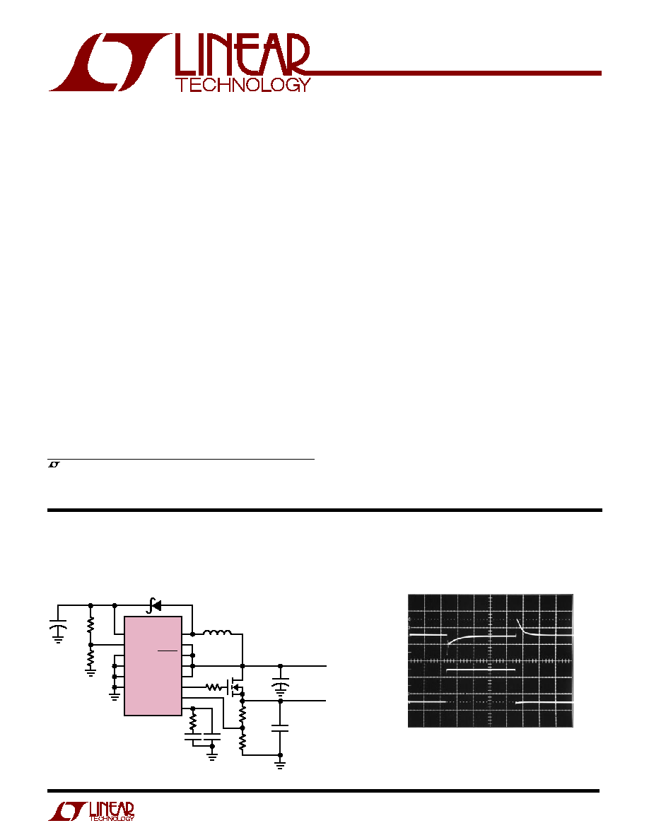
1.8V to 1.5V, 4A Very Low Dropout Linear Regulator
(Typical Dropout Voltage = 65mV at I
OUT
= 4A)
50mV/DIV
2A/DIV
20
µ
s/DIV
3150 TA02
Transient Response for
0.1A to 4A Output Load Step
s
Microprocessor, ASIC and I/O Supplies
s
Very Low Dropout Input-to-Output Conversion
s
Logic Termination Supplies
s
Fast Transient Response Optimized with
Ceramic Output Capacitors
s
FET R
DS(ON)
Defines Dropout Voltage
s
±
1% Reference Tolerance Over Temperature
s
Multifunction LDO Shutdown Pin with Latchoff
s
Fixed Frequency 1.4MHz Boost Converter Generates
MOSFET Gate Drive
s
Internally Compensated Boost Converter Uses Tiny
Capacitors and Inductor
s
Independent Boost Converter Shutdown Control
Permits LDO Output Voltage Supply Sequencing
s
16-Lead SSOP Package
The LT
®
3150 drives a low cost external N-channel MOSFET
as a source follower to produce a fast transient response,
very low dropout voltage linear regulator. Selection of the
N-channel MOSFET R
DS(ON)
allows dropout voltages below
300mV for low V
IN
to low V
OUT
applications.
The LT3150 includes a fixed frequency boost regulator
that generates gate drive for the N-channel MOSFET. The
internally compensated current mode PWM architecture
combined with the 1.4MHz switching frequency permits
the use of tiny, low cost capacitors and inductors.
The LT3150's transient load performance is optimized
with ceramic output capacitors. A precision 1.21V refer-
ence accommodates low voltage supplies.
Protection includes a high side current limit amplifier that
activates a fault timer circuit. A multifunction shutdown
pin provides either current limit time-out with latchoff,
overvoltage protection or thermal shutdown. Independent
shutdown control of the boost converter provides on/off
and sequencing control of the LDO output voltage.
+
V
IN2
FB1
SHDN2
SWGND
GND
GND
SW
V
IN1
SHDN1
I
POS
I
NEG
GATE
FB2
COMP
LT3150
MBR0520L
L1
10
µ
H
1.5k
C
IN
: PANASONIC SP SERIES EEFUE0E221R 20%
C1: AVX TAJA475M020R 20V 20%
L1: MURATA LQH32CN100K11 OR SUMIDA CDRH3D16100
243
1%
1020
1%
C1
4.7
µ
F
+
C
IN
220
µ
F
2.5V
×
2
V
IN
1.8V
V
OUT
1.5V
4A
6.19k
1%
1.37k
1%
Si4410
3150 TA01
2.2
µ
F
×
10
X5R CERAMIC
0805 CASE
5.1
6800pF
50pF
DESCRIPTIO
U
FEATURES
APPLICATIO S
U
TYPICAL APPLICATIO
U
, LTC and LT are registered trademarks of Linear Technology Corporation.
2
LT3150
3150f
(Note 1)
V
IN1
, SHDN1 Voltage .............................................. 10V
SW Voltage .............................................. 0.4V to 36V
FB1 Voltage ................................................ V
IN1
+ 0.3V
Current into FB1, FB2 Pin ....................................
±
1mA
V
IN2
, I
POS
, I
NEG
....................................................... 22V
SHDN2 .................................................................... V
IN2
Operating Ambient Temperature Range ..... 0
°
C to 70
°
C
Junction Temperature (Note 2) ........................... 125
°
C
Storage Temperature Range ................ 65
°
C to 150
°
C
Lead Temperature (Soldering, 10 sec)................. 300
°
C
ABSOLUTE AXI U RATI GS
W
W
W
U
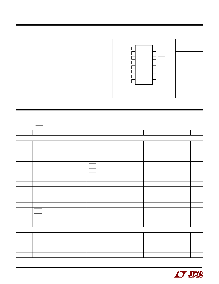
PACKAGE/ORDER I FOR ATIO
U
U
W
GN PACKAGE
16-LEAD PLASTIC SSOP
1
2
3
4
5
6
7
8
TOP VIEW
16
15
14
13
12
11
10
9
SW
SWGND
V
IN1
SHDN2
V
IN2
GND
NC
FB2
FB1
GND
SHDN1
I
POS
I
NEG
GATE
NC
COMP
ORDER PART
NUMBER
LT3150CGN
GN PART
MARKING
3150
T
JMAX
= 125
°
C,
JA
= 130
°
C/W,
JC
= 40
°
C/W
Consult LTC Marketing for parts specified with wider operating temperature ranges.
ELECTRICAL CHARACTERISTICS
The
q
denotes specifications which apply over the full operating temperature range, otherwise specifications are at T
A
= 25
°
C.
V
IN1
= 1.5V, V
SHDN1
= V
IN1
, V
IN2
= 12V, GATE = 6V, I
POS
= I
NEG
= 5V, V
SHDN2
= 0.75V unless otherwise noted.
SYMBOL
PARAMETER
CONDITIONS
MIN
TYP
MAX
UNITS
Boost Switching Regulator
V
IN1
Minimum Operating Voltage
0.9
1.1
V
V
IN1
Maximum Operating Voltage
10
V
V
FB1
FB1 Reference Voltage
q
1.20
1.23
1.255
V
FB1 Input Bias Current
Current Flows into Pin
q
27
80
nA
I
Q1
V
IN1
Quiescent Current
V
SHDN1
= 1.5V
3
4.5
mA
V
IN1
Quiescent Current in Shutdown
V
SHDN1
= 0V, V
IN1
= 2V
0.01
0.5
µ
A
V
SHDN1
= 0V, V
IN1
= 5V
0.01
1.0
µ
A
FB1 Reference Line Regulation
1.5V
V
IN1
10V
0.02
0.2
%/V
Switching Frequency
q
1
1.4
1.9
MHz
Maximum Duty Cycle
q
82
86
%
Switch Current Limit
(Note 3)
550
800
mA
Switch V
CESAT
I
SW
= 300mA
300
350
mV
Switch Leakage Current
V
SW
= 5V
0.01
1
µ
A
SHDN1 Input Voltage High
1
V
SHDN1 Input Voltage Low
0.3
V
SHDN1 Input Bias Current
V
SHDN1
= 3V, Current Flows into Pin
25
50
µ
A
V
SHDN1
= 0V, Current Flows into Pin
0.01
0.1
µ
A
Linear Regulator Controller
I
Q2
V
IN2
Quiescent Current
q
5
12
19
mA
V
FB2
FB2 Reference Voltage
1.203
1.210
1.217
V
q
1.198
1.210
1.222
V
FB2 Line Regulation
10V
V
IN2
20V
q
0.01
0.03
%/V
FB2 Input Bias Current
FB2 = V
FB2
,
Current Flows out of Pin
q
0.6
4
µ
A
3
LT3150
3150f
SYMBOL
PARAMETER
CONDITIONS
MIN
TYP
MAX
UNITS
A
VOL
Large-Signal Voltage Gain
V
GATE
= 3V to 10V
q
69
84
dB
V
OL
GATE Output Swing Low (Note 4)
I
GATE
= 0mA
q
2.5
3
V
V
OH
GATE Output Swing High
I
GATE
= 0mA
q
V
IN2
1.6
V
IN2
1
V
I
POS
+ I
NEG
Supply Current
3V
I
POS
20V
q
0.3
0.625
1
mA
Current Limit Threshold Voltage
42
50
58
mV
q
37
50
63
mV
Current Limit Threshold Voltage
3V
I
POS
20V
q
0.20
0.50
%/V
Line Regulation
SHDN2 Sink Current
Current Flows Into Pin
q
2.5
5.0
8.0
µ
A
SHDN2 Source Current
Current Flows Out of Pin
q
8
15
23
µ
A
SHDN2 Low Clamp Voltage
q
0.1
0.25
V
SHDN2 High Clamp Voltage
q
1.50
1.85
2.20
V
SHDN2 Threshold Voltage
q
1.18
1.21
1.240
V
SHDN2 Threshold Hysteresis
q
50
100
150
mV
Note 1: Absolute Maximum Ratings are those values beyond which the life
of the device may be impaired.
Note 2: T
J
is calculated from the ambient temperature T
A
and power
dissipation P
D
according to the following formula:
T
J
= T
A
+ (P
D
· 130
°
C/W)
ELECTRICAL CHARACTERISTICS
The
q
denotes specifications which apply over the full operating temperature range, otherwise specifications are at T
A
= 25
°
C.
V
IN1
= 1.5V, V
SHDN1
= V
IN1
, V
IN2
= 12V, GATE = 6V, I
POS
= I
NEG
= 5V, V
SHDN2
= 0.75V unless otherwise noted.
Note 3: Switch current limit is guaranteed by design and/or correlation to
static test.
Note 4: The V
GS(th)
of the external MOSFET must be greater than
3V V
OUT
.
4
LT3150
3150f
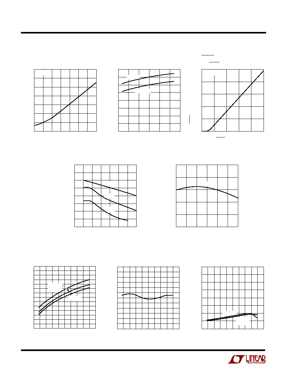
Switch V
CESAT
vs Switch Current
SHDN1 Input Bias Current
vs V
SHDN1
Oscillator Frequency
vs Temperature
FB2 Reference Voltage
vs Temperature
Switch Current Limit vs Duty Cycle
FB1 Reference Voltage
vs Temperature
FB2 Input Bias Current
vs Temperature
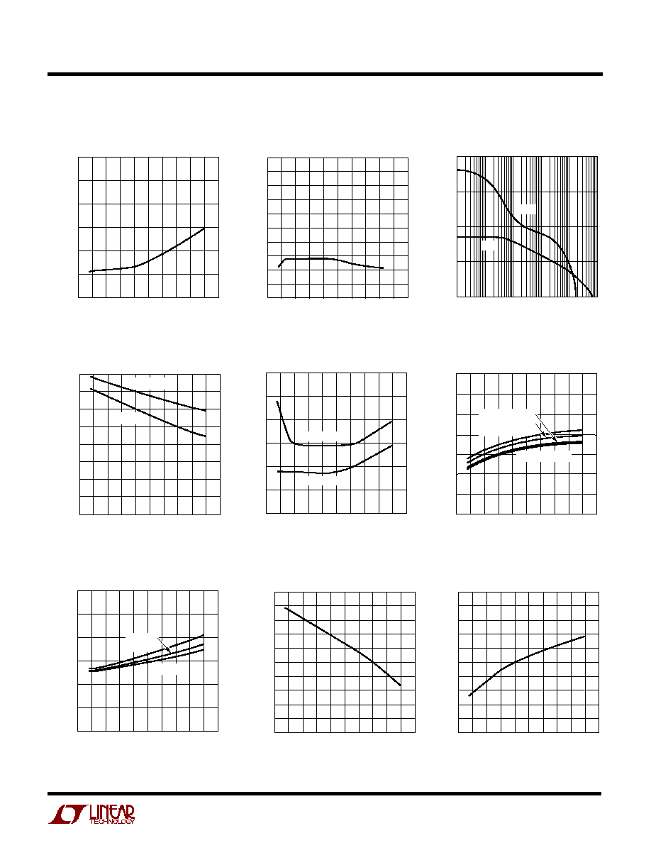
TYPICAL PERFOR A CE CHARACTERISTICS
U
W
SWITCH CURRENT (mA)
0
100
200
300
400
500
600
700
V
CESAT
(mV)
3150 G01
700
600
500
400
300
200
100
0
T
A
= 25
°
C
TEMPERATURE (
°
C)
50
25
0
25
50
75
100
SWITCHING FREQUENCY (MHz)
3150 G02
2.00
1.75
1.50
1.25
1.00
0.75
0.50
0.25
0
V
IN
= 5V
V
IN
= 1.5V
SHDN1 PIN VOLTAGE (V)
0
1
2
3
4
5
SHDN1 INPUT BIAS CURRENT (
µ
A)
3150 G03
50
40
30
20
10
0
T
A
= 25
°
C
DUTY CYCLE (%)
10
20
30
40
50
60
70
80
SWITCH CURRENT LIMIT (mA)
3150 G04
1000
900
800
700
600
500
400
300
200
70
°
C
25
°
C
40
°
C
TEMPERATURE (
°
C)
50
FB1 REFERENCE VOLTAGE (V)
3150 G05
1.25
1.24
1.23
1.22
1.21
1.20
VOLTAGE
25
0
25
50
75
100
TEMPERATURE (
°
C)
75
FB2 REFERENCE VOLTAGE (V)
1.210
1.214
1.218
1.222
125
3150 G07
1.206
1.202
1.208
1.212
1.216
1.220
1.204
1.200
1.198
25
25
75
50
150
0
50
100
175
TEMPERATURE (
°
C)
75
FB2 INPUT BIAS CURRENT (
µ
A)
3.0
4.0
125
3150 G08
2.0
1.0
2.5
3.5
1.5
0.5
0
25
25
75
50
150
0
50
100
175
V
IN
= 20V
V
IN
= 12V
V
IN
= 8V
Boost Switching Regulator
V
IN2
Quiescent Current
vs Temperature
TEMPERATURE (
°
C)
75
5
V
IN2
QUIESCENT CURRENT (mA)
7
9
11
19
15
25
25 50
150
17
13
6
8
10
18
14
16
12
50
0
75 100 125
175
3150 G06
V
IN
= 8V
V
IN
= 12V
V
IN
= 20V
Linear Regulator Controller
5
LT3150
3150f
Gain and Phase vs Frequency
Error Amplifier Large-Signal
Voltage Gain vs Temperature
Gate Output Swing High (V
IN2
V
GATE
) vs Temperature
I
POS
+ I
NEG
Supply Current
vs Temperature
Gate Output Swing Low
vs Temperature
Current Limit Threshold Voltage
vs Temperature
Current Limit Threshold Voltage
Line Regulation vs Temperature
TEMPERATURE (
°
C)
75
LARGE-SIGNAL VOLTAGE GAIN (dB)
105
115
125
3150 G10
95
85
100
110
120
90
80
75
70
25
25
75
50
150
0
50
100
175
FREQUENCY (Hz)
50
100
ERROR AMPLIFIER GAIN (dB) AND PHASE (DEG)
150
200
1k
100k
1M
100M
3150 G11
0
10k
10M
PHASE
GAIN
TEMPERATURE (
°
C)
75
GATE OUTPUT SWING LOW (V)
2.50
3.00
125
3150 G12
2.00
1.50
2.25
2.75
1.75
1.25
1.00
25
25
75
50
150
0
50
100
175
I
LOAD
= 50mA
NO LOAD
TEMPERATURE (
°
C)
0
GATE OUTPUT SWING HIGH (V)
1.0
2.0
3.0
0.5
1.5
2.5
25
25
75
125
3150 G13
175
50
75
0
50
100
150
NO LOAD
I
LOAD
= 50mA
TEMPERATURE (
°
C)
75
300
I
POS
+ I
NEG
SUPPLY CURRENT (
µ
A)
400
600
700
800
1000
50
50
100
3150 G14
500
900
25
150 175
25 0
75
125
I
POS
= I
NEG
= 3V
I
POS
= I
NEG
= 5V
I
POS
= I
NEG
= 12V
I
POS
= I
NEG
= 20V
TEMPERATURE (
°
C)
35
CURRENT LIMIT THRESHOLD VOLTAGE (mV)
45
55
65
40
50
60
25
25
75
125
3150 G15
175
50
75
0
50
100
150
I
POS
= 5V
I
POS
= 3V
I
POS
= 20V
TEMPERATURE (
°
C)
75
CURRENT LIMIT THRESHOLD
VOLTAGE LINE REGULATION (%/V)
0.2
0.1
0
125
3150 G16
0.3
0.4
0.5
25
25
75
50
150
0
50
100
175
SHDN2 Sink Current
vs Temperature
TEMPERATURE (
°
C)
75
SHDN2 SINK CURRENT (
µ
A)
5.5
6.5
7.5
125
3150 G17
4.5
3.5
5.0
6.0
7.0
4.0
3.0
2.5
25
25
75
50
150
0
50
100
175
TYPICAL PERFOR A CE CHARACTERISTICS
U
W
FB2 Line Regulation
vs Temperature
TEMPERATURE (
°
C)
0
FB2 LINE REGULATION (%/
V)
0.010
0.020
0.030
0.005
0.015
0.025
25
25
75
125
3150 G09
175
50
75
0
50
100
150
Linear Regulator Controller