
LT1952
1
1952f
APPLICATIO S
U
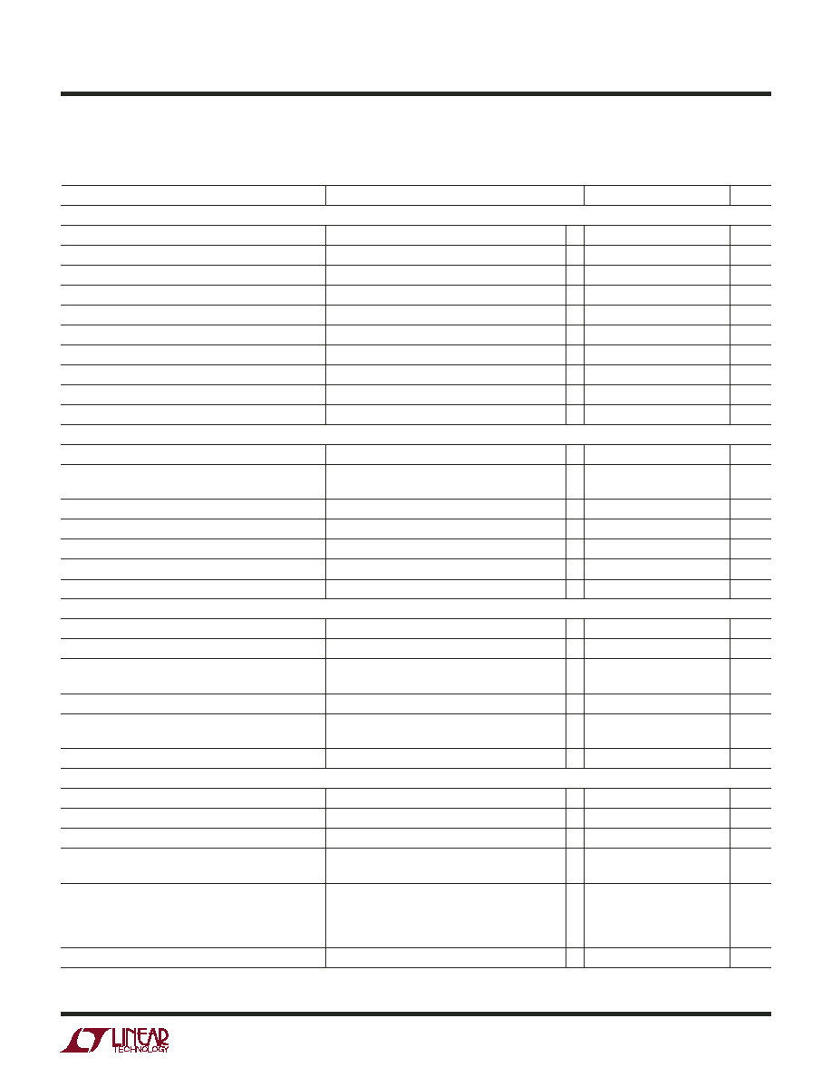
TYPICAL APPLICATIO
U
DESCRIPTIO
U
FEATURES
The LT
®
1952 is a current mode PWM controller optimized
to control the forward converter topology, using one
primary MOSFET. The LT1952 provides synchronous
rectifier control, resulting in extremely high efficiency. A
programmable Volt-Second clamp provides a safeguard
for transformer reset that prevents saturation. This allows
a single MOSFET on the primary side to reliably run at
greater than 50% duty cycle for high MOSFET, trans-
former and rectifier utilization. The LT1952 includes
soft-start for controlled exit from shutdown, overcurrent
conditions and undervoltage lockout. A precision 100mV
current limit threshold, independent of duty cycle, com-
bines with soft-start to provide hiccup short circuit protec-
tion. Micropower start-up allows the LT1952 to be effi-
ciently started from high input voltages. Programmable
slope compensation and leading edge blanking allow
optimization of loop bandwidth with a wide range of
inductors and MOSFETs. The LT1952 can be programmed
over a 100kHz to 500kHz frequency range and the part can
be synchronized to an external clock. The error amplifier
is a true op amp, allowing a wide range of compensation
networks. The LT1952 is available in a small 16-pin SSOP
package.
Telecommunications Power Supplies
Industrial and Distributed Power
Isolated and Non-Isolated DC/DC Converters
, LTC and LT are registered trademarks of Linear Technology Corporation.
Synchronous Rectifier Control for High Efficiency
Programmable Volt-Second Clamp
Output Power Levels from 25W to 500W
Low Current Start-Up
True PWM Soft-Start
Low Stress Short Circuit Protection
Precision 100mV Current Limit Threshold
Adjustable Delay for Synchronous Timing
Accurate Shutdown Threshold with Programmable
Hysteresis
Programmable Slope Compensation
Programmable Leading Edge Blanking
Programmable Frequency (100kHz to 500kHz)
Synchronizable to an External Clock up to 1.5 · f
OSC
Internal 1.23V Reference
2.5V External Reference
Current Mode Control
Small 16-Pin SSOP Package
Single Switch Synchronous
Forward Controller
36V to 72V Input, 12V at 20A Semi-Regulated Bus Converter
V
IN
V
IN
T1
PA0905
SUPPLY FROM BIAS
WINDING OF T1
Si7370
×2
PH4840
×2
L1
PA1494.242
47µF
16V
X5R
×2
V
OUT
12V
20A
220pF
560
T2
1952 TA01
V
REF
COMP
SS_MAXDC
SD_V
SEC
FB
SYNC
GND
V
IN
OUT
OC
I
SENSE
SOUT
LT1952
BLANK DELAY
R
OSC
0.1µF
40k
16V
340k
13k
52.3k
40k
40k
PGND
178k
100k
Si7450
0.005
SYNC
FG
CG
LTC3900
10µF
0.1µF
12V Bus Converter
V
OUT
vs V
IN
V
IN
(V)
36
8
V
OUT
(V)
10
16
48
60
66
1952 TA01b
14
12
42
54
72

LT1952
2
1952f
GN PACKAGE
16-LEAD PLASTIC SSOP
1
2
3
4
5
6
7
8
TOP VIEW
16
15
14
13
12
11
10
9
COMP
FB
R
OSC
SYNC
SS_MAXDC
V
REF
SD_V
SEC
GND
SOUT
V
IN
OUT
PGND
DELAY
OC
I
SENSE
BLANK
V
IN
(Note 8) ............................................... 0.3V to 25V
SYNC, SS_MAXDC, SD_V
SEC
, I
SENSE
,
OC, COMP, BLANK, DELAY ......................... 0.3V to 6V
FB ................................................................ 0.3V to 3V
R
OSC ......................................................................................
50µA
V
REF
.................................................................... 10mA
Operating Junction Temperature Range
(Notes 2, 5) ....................................... 40°C to 125°C
Storage Temperature Range ................. 65°C to 150°C
Lead Temperature (Soldering, 10 sec).................. 300°C
ORDER PART
NUMBER
GN PART
MARKING
T
JMAX
= 125°C,
JA
= 110°C/W,
JC
= 40°C/W
Consult LTC Marketing for parts specified with wider operating temperature ranges.
1952E
1952I
LT1952EGN
LT1952IGN
ABSOLUTE AXI U
RATI GS
W
W
W
U
PACKAGE/ORDER I FOR ATIO
U
U
W
(Note 1)
ELECTRICAL CHARACTERISTICS
The
denotes the specifications which apply over the full operating
temperature range, otherwise specifications are at T
A
= 25°C. COMP = open, FB = 1.4V, R
OSC
= 178k, SYNC = 0V, SS_MAXDC = V
REF
, V
REF
= 0.1µF, SD_V
SEC
= 2V, BLANK = 40k, DELAY = 40k, I
SENSE
= 0V, OC = 0V, OUT = 1nF, V
IN
= 15V, SOUT = open, unless otherwise specified.
PARAMETER
CONDITIONS
MIN
TYP
MAX
UNITS
PWM CONTROLLER
Operational Input Voltage
I
(VREF)
= 0µA
V
IN OFF
25
V
V
IN
Quiescent Current
I
(VREF)
= 0µA, FB = 0V, I
SENSE
= OC = Open
5.2
6.5
mA
V
IN
Startup Current
FB = 0V, SS_MAXDC = 0V (Notes 4, 9)
460
700
µA
V
IN
Shutdown Current
SD_V
SEC
= 0V
240
350
µA
SD_V
SEC
Threshold
10V < V
IN
< 25V
1.261
1.32
1.379
V
SD_V
SEC (ON)
Current
SD_V
SEC
= SD_V
SEC
Threshold + 100mV
0
µA
SD_V
SEC (OFF)
Current
SD_V
SEC
= SD_V
SEC
Threshold 100mV
9.5
11.2
12.9
µA
V
IN ON
12.75
14.25
15.75
V
V
IN OFF
8.0
8.75
9.25
V
V
IN HYSTERESIS
3.75
5.5
6.75
V
V
REF
Output Voltage
I
(VREF)
= 0µA
2.425
2.5
2.575
V
Line Regulation
I
(VREF)
= 0µA, 10V < V
IN
< 25V
1
10
mV
Load Regulation
0µA < I
(VREF)
< 2.5mA
1
10
mV
OSCILLATOR
Frequency: f
OSC
R
OSC
= 178k, FB = 1V
165
200
240
kHz
Minimum Programmable f
OSC
R
OSC
= 365k
80
100
120
kHz
Maximum Programmable f
OSC
R
OSC
= 64.9k, COMP = 2.5V, SD_V
SEC
= 2.64V
440
500
560
kHz
SYNC Input Resistance
18
k
SYNC Switching Threshold
FB = 1V
1.5
2.2
V
SYNC Frequency/f
OSC
FB = 1V (Note 7)
1.25
1.5
f
OSC
Line Reg
FB = 1V, R
OSC
= 178k; 10V < V
IN
< 25V,
0.05
0.33
%/V
SS_MAXDC = 1.84V
V
ROSC
R
OSC
Pin voltage
1
V
LT1952
3
1952f
ELECTRICAL CHARACTERISTICS
The
denotes the specifications which apply over the full operating
temperature range, otherwise specifications are at T
A
= 25°C. COMP = open, FB = 1.4V, R
OSC
= 178k, SYNC = 0V, SS_MAXDC = V
REF
,
V
REF
= 0.1µF, SD_V
SEC
= 2V, BLANK = 40k, DELAY = 40k, I
SENSE
= 0V, OC = 0V, OUT = 1nF, V
IN
= 15V, SOUT = open, unless otherwise
specified.
PARAMETER
CONDITIONS
MIN
TYP
MAX
UNITS
ERROR AMPLIFIER
FB Reference Voltage
10V < V
IN
< 25V, V
OL
+ 0.2V < COMP < V
OH
0.2
1.201
1.226
1.250
V
FB Input Bias Current
FB = FB Reference Voltage
75
200
nA
Open Loop Voltage Gain
V
OL
+ 0.2V < COMP < V
OH
0.2
65
85
dB
Unity Gain Bandwidth
(Note 6)
3
MHz
COMP Source Current
FB = 1V, COMP = 1.6V
4
9
mA
COMP Sink Current
COMP = 1.6V
4
10
mA
COMP Current (Disabled)
FB = V
REF
, COMP = 1.6V
18
23
28
µA
COMP High Level: V
OH
FB = 1V, I
(COMP)
= 250µA
2.7
3.2
V
COMP Active Threshold
FB = 1V, SOUT Duty Cycle > 0 %
0.7
1.0
V
COMP Low Level: V
OL
I
(COMP)
= 250µA
0.15
0.4
V
CURRENT SENSE
I
SENSE
Maximum Threshold
COMP = 2.5V, FB = 1V
197
220
243
mV
I
SENSE
Input Current (Duty Cycle = 0%)
COMP = 2.5V, FB = 1V (Note 4)
8
µA
I
SENSE
Input Current (Duty Cycle = 80%)
COMP = 2.5V, FB = 1V (Note 4)
35
µA
OC Threshold
98
107
116
mV
OC Input Current
(OC = 100mV)
50
100
nA
Default Blanking Time
COMP = 2.5V, FB = 1V (Note 10)
180
ns
Adjustable Blanking Time
COMP = 2.5V, FB = 1V, R
BLANK
= 120k
540
ns
V
BLANK
1
V
SOUT DRIVER
SOUT Clamp Voltage
I
(GATE)
= 0µA, COMP = 2.5V, FB = 1V
10.5
12
13.5
V
SOUT Low Level
I
(GATE)
= 25mA
0.5
0.75
V
SOUT High Level
I
(GATE)
= 25mA, V
IN
= 12V, COMP = 2.5V,
10
V
FB = 1V
SOUT Active Pull-Off in Shutdown
V
IN
= 5V, SD_V
SEC
= 0V, SOUT = 1V
1
mA
SOUT to OUT (Rise) DELAY (t
DELAY
)
COMP = 2.5V, FB = 1V (Note 10)
40
ns
R
DELAY
= 120k
120
ns
V
DELAY
0.9
V
OUT DRIVER
OUT Rise Time
FB = 1V, CL = 1nF (Notes 3, 6)
50
ns
OUT Fall Time
FB = 1V, CL = 1nF (Notes 3, 6)
30
ns
OUT Clamp Voltage
I
(GATE)
= 0µA, COMP = 2.5V, FB = 1V
11.5
13
14.5
V
OUT Low Level
I
(GATE)
= 20mA
0.45
0.75
V
I
(GATE)
= 200mA
1.25
1.8
V
OUT High Level
I
(GATE)
= 20mA, V
IN
= 12V, COMP = 2.5V,
9.9
V
FB = 1V
I
(GATE)
= 200mA, V
IN
= 12V, COMP = 2.5V,
9.75
V
FB = 1V
OUT Active Pull-Off in Shutdown
V
IN
= 5V, SD_V
SEC
= 0V, OUT = 1V
20
mA

LT1952
4
1952f
ELECTRICAL CHARACTERISTICS
The
denotes the specifications which apply over the full operating
temperature range, otherwise specifications are at T
A
= 25°C. COMP = open, FB = 1.4V, R
OSC
= 178k, SYNC = 0V, SS_MAXDC = V
REF
,
V
REF
= 0.1µF, SD_V
SEC
= 2V, BLANK = 40k, DELAY = 40k, I
SENSE
= 0V, OC = 0V, OUT = 1nF, V
IN
= 15V, SOUT = open, unless otherwise
specified.
PARAMETER
CONDITIONS
MIN
TYP
MAX
UNITS
Note 1: Absolute Maximum Ratings are those values beyond which the life
of a device may be impaired.
Note 2: The LT1952EGN is guaranteed to meet performance specifications
from 0°C to 125°C junction temperature. Specifications over the 40°C to
125°C operating junction temperature range are assured by design,
characterization and correlation with statistical process controls. The
LT1952IGN is guaranteed over the full 40°C to 125°C operating junction
temperature range.
Note 3: Rise and Fall times are measured at 10% and 90% levels.
Note 4: Guaranteed by correlation to static test.
Note 5: This IC includes over-temperature protection that is intended to
protect the device during momentary overload conditions. Junction
temperature will exceed 125°C when over-temperature protection is active.
Continuous operation above the specified maximum operating junction
temperature may impair device reliability.
Note 6: Guaranteed but not tested.
Note 7: Maximum recommended SYNC frequency = 500kHz.
Note 8: In applications where the V
IN
pin is supplied via an external RC
network from a SYSTEM V
IN
> 25V, an external zener with clamp voltage
V
IN ON(MAX)
< V
Z
< 25V should be connected from the V
IN
pin to ground.
Note 9: V
IN
start-up current is measured at V
IN
= V
IN ON
0.25V and
scaled by x 1.18 (to correlate to worst case V
IN
start-up current at V
IN ON
).
Note 10: Timing for R = 40k derived from measurement with R = 240k.
OUT Max Duty Cycle
COMP = 2.5V, FB = 1V, R
DELAY
= 10k
(f
OSC
= 200kHz)
SD_V
SEC
= 1.4V, SS_MAXDC = V
REF
83
90
%
OUT Max Duty Cycle Clamp
COMP = 2.5V, FB = 1V, R
DELAY
= 10k
(f
OSC
= 200kHz)
SD_V
SEC
= 1.32V, SS_MAXDC = 1.84V
63.5
72
80.5
%
SD_V
SEC
= 2.64V, SS_MAXDC = 1.84V
25
33
41
%
SOFT-START
SS_MAXDC Low Level: V
OL
I
(SS_MAXDC)
= 150µA, OC = 1V
0.2
V
SS_MAXDC Soft-Start Reset Threshold
Measured on SS_MAXDC
0.45
V
SS_MAXDC Active Threshold
FB = 1V, DC > 0%
0.8
V
SS_MAXDC Input Current (Soft-Start Pulldown: Idis)
SS_MAXDC = 1V, SD_V
SEC
= 1.4V, OC = 1V
800
µA
LT1952
5
1952f
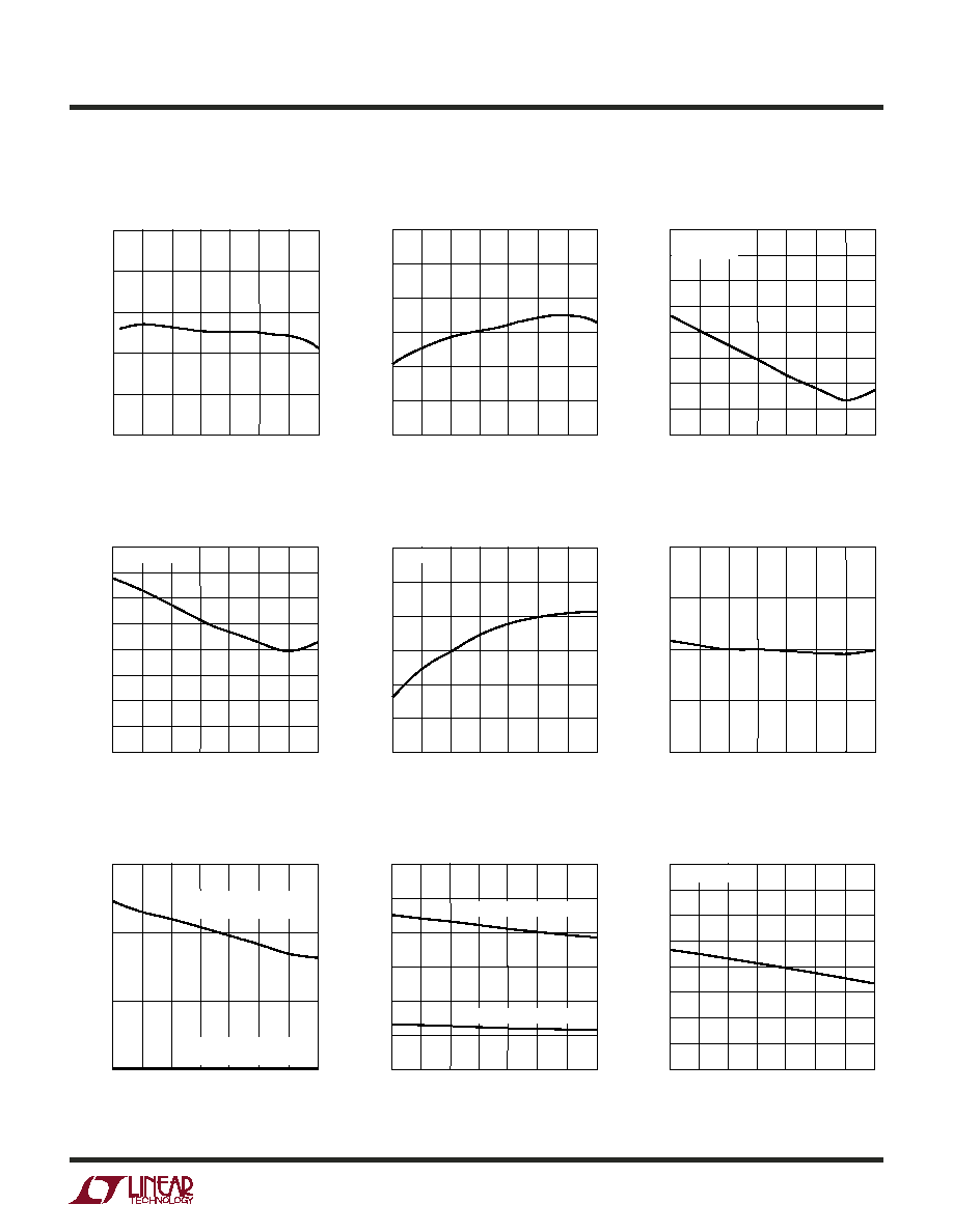
TYPICAL PERFOR A CE CHARACTERISTICS
U
W
V
IN
Start-up Current vs
Temperature
V
IN
I
Q
vs Temperature
SD_V
SEC
Turn ON Threshold vs
Temperature
SD_V
SEC
Pin Current vs
Temperature
V
IN
Turn ON/OFF Voltage vs
Temperature
COMP Active Threshold vs
Temperature
FB Voltage vs Temperature
Switching Frequency vs
Temperature
V
IN
Shutdown Current vs
Temperature
TEMPERATURE (°C)
50
1.20
FB VOLTAGE (V)
1.22
1.25
0
50
75
1952 G01
1.21
1.24
1.23
25
25
100
125
TEMPERATURE (°C)
50
155
SWITCHING FREQUENCY (kHz)
185
245
0
50
75
1952 G02
170
230
215
200
25
25
100
125
TEMPERATURE (°C)
50
100
V
IN
SHUTDOWN CURRENT (
µ
A)
200
500
0
50
75
1952 G03
150
400
300
450
350
250
25
25
100
125
V
IN
= 15V
SD_V
SEC
= 0V
TEMPERATURE (°C)
50
V
IN
STARTUP CURRENT (
µ
A)
200
500
0
50
75
1952 G04
400
300
450
600
550
350
250
25
25
100
125
SD_V
SEC
= 1.4V
TEMPERATURE (°C)
50
3.5
V
IN
I
Q
(mA)
4.5
6.5
0
50
75
1952 G05
4.0
6.0
5.5
5.0
25
25
100
125
OC = OPEN
TEMPERATURE (°C)
50
1.22
SD_V
SEC
TURN ON THRESHOLD (V)
1.27
1.42
0
50
75
1952 G06
1.37
1.32
25
25
100
125
TEMPERATURE (°C)
50
0
SD_V
SEC
PIN CURRENT (
µ
A)
15
0
50
75
1952 G07
10
5
25
25
100
125
0µA PIN CURRENT AFTER
PART TURN ON
PIN CURRENT BEFORE
PART TURN ON
TEMPERATURE (°C)
50
6
8
V
IN
(V)
18
16
14
12
0
50
75
1952 G08
10
25
25
100
125
V
IN
TURN OFF VOLTAGE
V
IN
TURN ON VOLTAGE
TEMPERATURE (°C)
50
0
COMP (V)
0.4
1.6
1.4
1.2
0
50
75
1952 G09
0.2
1.0
0.8
0.6
25
25
100
125
R
ISENSE
= 0k