Äîêóìåíòàöèÿ è îïèñàíèÿ www.docs.chipfind.ru
1
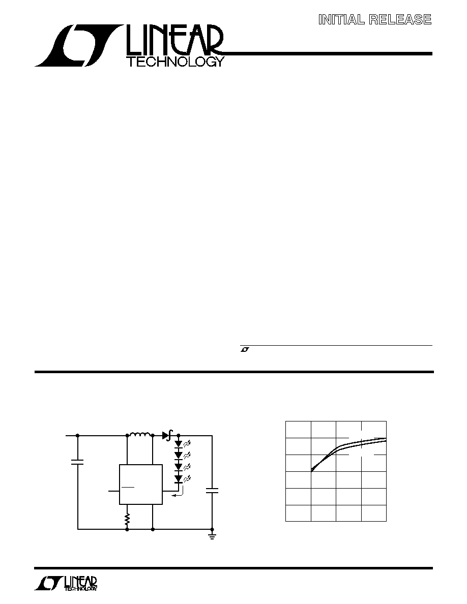
LT1932
Constant-Current DC/DC
LED Driver in ThinSOT
July 2001
The LT
®
1932 is a fixed frequency step-up DC/DC converter
designed to operate as a constant-current source. Be-
cause it directly regulates output current, the LT1932 is
ideal for driving light emitting diodes (LEDs) whose light
intensity is proportional to the current passing through
them, not the voltage across their terminals.
With an input voltage range of 1V to 10V, the device works
from a variety of input sources. The LT1932 accurately
regulates LED current even when the input voltage is
higher than the LED voltage, greatly simplifying battery-
powered designs. A single external resistor sets LED
current between 5mA and 40mA, which can then be easily
adjusted using either a DC voltage or a pulse width
modulated (PWM) signal. When the LT1932 is placed in
shutdown, the LEDs are disconnected from the output,
ensuring a quiescent current of under 1
µ
A for the entire
circuit. The device's 1.2MHz switching frequency permits
the use of tiny, low profile chip inductors and capacitors to
minimize footprint and cost in space-conscious portable
applications.
s
Up to 80% Efficiency
s
Inherently Matched LED Current
s
Drives Five White LEDs from 2V
s
Drives Six White LEDs from 2.7V
s
Drives Eight White LEDs from 3V
s
Precise, Adjustable Control of LED Current
s
Disconnects LEDs In Shutdown
s
1.2MHz Fixed Frequency Switching
s
Uses Tiny Ceramic Capacitors
s
Uses Tiny 1mm-Tall Inductors
s
Regulates Current Even When V
IN
> V
OUT
s
Operates with V
IN
as Low as 1V
s
Low Profile (1mm) ThinSOT
TM
Package
s
Cellular Telephones
s
Handheld Computers
s
Digital Cameras
s
Portable MP3 Players
s
Pagers
Information furnished by Linear Technology Corporation is believed to be accurate and reliable.
However, no responsibility is assumed for its use. Linear Technology Corporation makes no represen-
tation that the interconnection of its circuits as described herein will not infringe on existing patent rights.
FEATURES
DESCRIPTIO
U
APPLICATIO S
U
TYPICAL APPLICATIO
U
Li-Ion Driver for Four White LEDs
Efficiency
Final Electrical Specifications
, LTC and LT are registered trademarks of Linear Technology Corporation.
V
IN
SW
D1
15mA
1932 TA01
L1
6.8
µ
H
V
IN
2.7V TO 4.2V
LT1932
SHDN
C1: TAIYO YUDEN JMK212BJ475
C2: TAIYO YUDEN EMK212BJ105
D1:ZETEX ZHCS400
L1: SUMIDA CLQ4D106R8 OR PANASONIC ELJEA6R8
6
1
4
R
SET
1.50k
PWM
DIMMING
CONTROL
C1
4.7
µ
F
C2
1
µ
F
2
3
5
LED
R
SET
GND
LED CURRENT (mA)
0
55
EFFICIENCY (%)
60
65
70
75
80
85
5
10
15
20
1932 TA02
V
IN
= 4.2V
V
IN
= 2.7V
ThinSOT is a trademark of Linear Technology Corporation.
2
LT1932
PARAMETER
CONDITIONS
MIN
TYP
MAX
UNITS
Minimum Input Voltage
1
V
Quiescent Current
V
RSET
= 0.2V
1.2
1.6
mA
V
SHDN
= 0V
0.1
1.0
µ
A
R
SET
Pin Voltage
R
SET
= 1.50k
100
mV
LED Pin Voltage
R
SET
= 1.50k, V
IN
< V
OUT
(Figure 1)
120
180
mV
LED Pin Current
R
SET
= 562
, V
IN
= 1.5V
34
38
42
mA
R
SET
= 750
, V
IN
= 1.2V
26
30
34
mA
R
SET
= 1.50k, V
IN
= 1.2V
12.5
15
17.5
mA
R
SET
= 4.53k, V
IN
= 1.2V
5
mA
LED Pin Current Temperature Coefficient
I
LED
= 15mA
0.02
mA/
°
C
Switching Frequency
V
IN
= 1V
0.8
1.2
1.6
MHz
Maximum Switch Duty Cycle
q
90
95
%
Switch Current Limit
400
550
780
mA
Switch V
CESAT
I
SW
= 300mA
150
200
mV
SHDN Pin Current
V
SHDN
= 0V
0
0.1
µ
A
V
SHDN
= 2V
15
30
µ
A
Start-Up Threshold (SHDN Pin)
0.85
V
Shutdown Threshold (SHDN Pin)
0.25
V
Switch Leakage Current
Switch Off, V
SW
= 5V
0.01
5
µ
A
(Note 1)
V
IN
Voltage ............................................................. 10V
SHDN Voltage ......................................................... 10V
SW Voltage ............................................................. 36V
LED Voltage ............................................................. 36V
R
SET
Voltage ............................................................. 1V
Junction Temperature .......................................... 125
°
C
Operating Temperature Range (Note 2) .. 40
°
C to 85
°
C
Storage Temperature Range ................. 65
°
C to 150
°
C
Lead Temperature (Soldering, 10 sec).................. 300
°
C
ORDER PART
NUMBER
LT1932ES6
T
JMAX
= 125
°
C,
JA
= 250
°
C/ W
The
q
denotes specifications that apply over the full operating temperature
range, otherwise specifications are at T
A
= 25
°
C. V
IN
= 1.2V, V
SHDN
= 1.2V, unless otherwise noted.
ABSOLUTE AXI U RATI GS
W
W
W
U
PACKAGE/ORDER I FOR ATIO
U
U
W
ELECTRICAL CHARACTERISTICS
S6 PART MARKING
LTST
SW 1
GND 2
LED 3
6 V
IN
5 SHDN
4 R
SET
TOP VIEW
S6 PACKAGE
6-LEAD PLASTIC SOT-23
Note 1: Absolute Maximum Ratings are those values beyond which the life of
a device may be impaired.
Note 2: The LT1932E is guaranteed to meet specifications from 0
°
C to 70
°
C.
Specifications over the 40
°
C to 85
°
C operating temperature range are
assured by design, characterization and correlation with statistical process
controls.
Consult LTC Marketing for parts specified with wider operating temperature
ranges.
3
LT1932
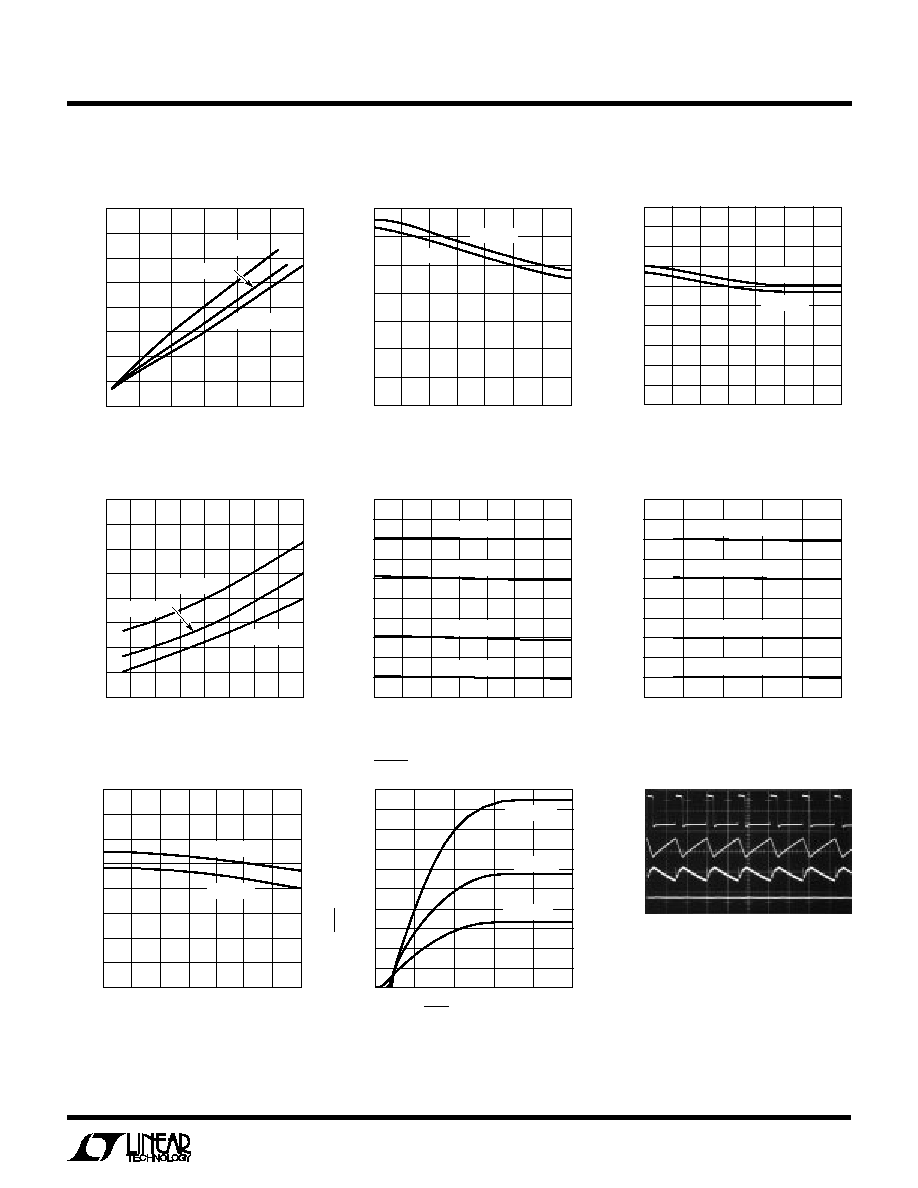
TYPICAL PERFOR A CE CHARACTERISTICS
U
W
Switch Saturation Voltage (V
CESAT
)
SWITCH CURRENT (mA)
0
SWITCH SATURATION VOLTAGE (mV)
150
200
250
300
500
1932 G01
100
50
0
100
200
400
300
350
400
600
T
J
= 125
°
C
T
J
= 50
°
C
T
J
= 25
°
C
TEMPERATURE (
°
C)
50
400
500
700
25
75
1932 G02
300
200
25
0
50
100
125
100
0
600
PEAK CURRENT (mA)
V
IN
= 1.2V
V
IN
= 10V
TEMPERATURE (
°
C)
50
0
SWITCHING FREQUENCY (MHz)
0.2
0.6
0.8
1.0
2.0
1.4
0
50
75
1932 G03
0.4
1.6
1.8
1.2
25
25
100
125
V
IN
= 1.2V
V
IN
= 10V
Switch Current Limit
Switching Frequency
LED Pin Voltage
LED Current
LED CURRENT (mA)
0
LED PIN VOLTAGE (mV)
150
200
250
15
25
1932 G04
100
50
0
5
10
20
300
350
400
40
30
35
T
J
= 125
°
C
T
J
= 25
°
C
T
J
= 50
°
C
TEMPERATURE (
°
C)
50
LED CURRENT (mA)
35
25
1932 G05
20
10
25
0
50
5
0
40
45
50
30
25
15
75
100
125
R
SET
= 750
R
SET
= 562
R
SET
= 1.50k
R
SET
= 4.53k
Quiescent Current
SHDN Pin Current
LED Current
INPUT VOLTAGE (V)
0
LED CURRENT (mA)
35
6
1932 G06
20
10
2
4
5
0
40
45
50
30
25
15
8
10
R
SET
= 750
R
SET
= 562
R
SET
= 1.50k
R
SET
= 4.53k
TEMPERATURE (
°
C)
50
QUIESCENT CURRENT (mA)
1.75
25
1932 G07
1.00
0.50
25
0
50
0.25
0
2.00
1.50
1.25
0.75
75
100
125
V
IN
= 1.2V
V
IN
= 10V
SHDN PIN VOLTAGE (V)
0
SHDN PIN CURRENT
30
40
50
8
1932 G08
20
10
25
35
45
15
5
0
2
4
6
10
T
J
= 125
°
C
T
J
= 25
°
C
T
J
= 50
°
C
Switching Waveforms
V
SW
10V/DIV
I
L1
200mA/DIV
V
OUT
20mV/DIV
AC COUPLED
I
LED
10mA/DIV
V
IN
= 3V
0.5
µ
s/DIV
1093 G09
4 WHITE LEDs
I
LED
= 15mA
CIRCUIT ON FIRST PAGE
OF THIS DATA SHEET
4
LT1932
BLOCK DIAGRA
W
+
1
3
×
5
1.2MHz
OSCILLATOR
DRIVER
S
Q
R
+
A2
+
A1
0.04
+
+
Q1
Q2
LED
SW
D1
6
V
IN
L1
5
SHDN
C1
C2
V
OUT
V
IN
DRIVER
LED CURRENT
REFERENCE
I
LED
4
R
SET
1932 F01
R
SET
I
SET
2
GND
Figure 1. LT1932 Block Diagram
OPERATIO
U
The LT1932 uses a constant frequency, current mode
control scheme to regulate the output current, I
LED
.
Operation can be best understood by referring to the
block diagram in Figure 1. At the start of each oscillator
cycle, the SR latch is set, turning on power switch Q1. The
signal at the noninverting input of the PWM comparator
A2 is proportional to the switch current, summed to-
gether with a portion of the oscillator ramp. When this
signal reaches the level set by the output of error amplifier
A1, comparator A2 resets the latch and turns off the
power switch. In this manner, A1 sets the correct peak
current level to keep the LED current in regulation. If A1's
output increases, more current is delivered to the output;
if it decreases, less current is delivered. A1 senses the
LED current in switch Q2 and compares it to the current
reference, which is programmed using resistor R
SET
. The
R
SET
pin is regulated to 100mV and the output current,
I
LED
, is regulated to 225 · I
SET
. Pulling the R
SET
pin higher
than 100mV will pull down the output of A1, turning off
power switch Q1 and LED switch Q2.
U
U
U
PI FU CTIO S
SW (Pin 1): Switch Pin. This is the collector of the internal
NPN power switch. Minimize the metal trace area con-
nected to this pin to minimize EMI.
GND (Pin 2): Ground Pin. Tie this pin directly to local
ground plane.
LED (Pin 3): LED Pin. This is the collector of the internal
NPN LED switch. Connect the cathode of the bottom LED
to this pin.
R
SET
(Pin 4): A resistor between this pin and ground
programs the LED current (that flows into the LED pin).
This pin is also used to provide LED dimming.
SHDN (Pin 5): Shutdown Pin. Tie this pin higher than
0.85V to turn on the LT1932; tie below 0.25V to turn it off.
V
IN
(Pin 6): Input Supply Pin. Bypass this pin with a
capacitor to ground as close to the device as possible.
5
LT1932
APPLICATIO S I FOR ATIO
W
U
U
U
Inductor Selection
Several inductors that work well with the LT1932 are listed
in Table 1. Many different sizes and shapes are available.
Consult each manufacturer for more detailed information
and for their entire selection of related parts. As core
losses at 1.2MHz are much lower for ferrite cores that for
the cheaper powdered-iron ones, ferrite core inductors
should be used to obtain the best efficiency. Choose an
inductor that can handle at least 0.5A and ensure that the
inductor has a low DCR (copper wire resistance) to mini-
mize I
2
R power losses. A 4.7
µ
H or 6.8
µ
H inductor will be
a good choice for most LT1932 designs.
Table 1. Recommended Inductors
MAX
MAX
L
DCR
HEIGHT
PART
(
µ
H)
(m
)
(mm)
VENDOR
ELJEA4R7
4.7
180
2.2
Panasonic
ELJEA6R8
6.8
250
2.2
(714) 373-7334
www.panasonic.com
LQH3C4R7M24
4.7
260
2.2
Murata
LQH3C100M24
10
300
2.2
(814) 237-1431
www.murata.com
LB2016B4R7
4.7
250
2.0
Taiyo Yuden
LB2016B100
6.8
350
2.0
(408) 573-4150
www.t-yuden.com
CMD4D06-4R7
4.7
216
0.8
Sumida
CMD4D06-6R8
6.8
296
0.8
(847) 956-0666
CLQ4D10-4R7
4.7
162
1.2
www.sumida.com
CLQ4D10-6R8
6.8
195
1.2
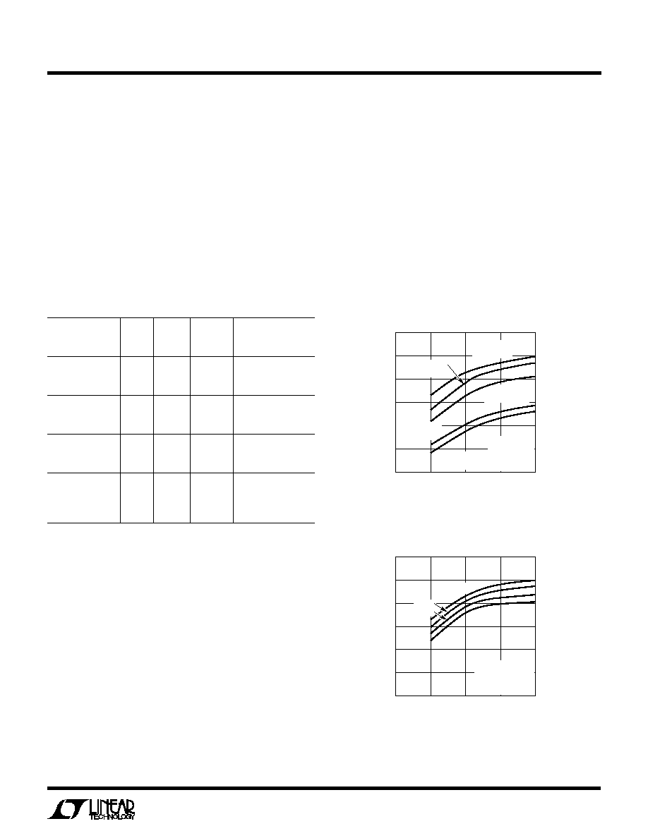
Inductor Efficiency Considerations
Many applications have thickness requirements that re-
strict component heights to 1mm or 2mm. There are 2mm
tall inductors currently available that provide a low DCR
and low core losses that help provide good overall effi-
ciency. Inductors with a height of 1mm (and less) are
becoming more common, and a few companies have
introduced chip inductors that are not only thin, but have
a very small footprint as well. While these smaller induc-
tors will be a necessity in some designs, their smaller size
gives higher DCR and core losses, resulting in lower
efficiencies. Figure 2 shows efficiency for the Typical
Application circuit on the front page of this data sheet, with
several different inductors. The larger devices improve
efficiency by up to 12% over the smaller, thinner ones.
Keep this in mind when choosing an inductor.
The value of inductance also plays an important role in the
overall system efficiency. While a 1
µ
H inductor will have
a lower DCR and a higher current rating than the 6.8
µ
H
version of the same part, lower inductance will result in
higher peak currents in the switch, inductor and diode.
Efficiency will suffer if inductance is too small. Figure 3
shows the efficiency of the Typical Application on the front
page of this data sheet, with several different values of the
same type of inductor (Panasonic ELJEA). The smaller
values give an efficiency 3% to 5% lower than the 6.8
µ
H
value.
Figure 2. Efficiency for Several Different Inductor Types
Figure 3. Efficiency for Several Different Inductor Values
LED CURRENT (mA)
0
55
EFFICIENCY (%)
60
65
70
75
80
85
5
10
15
20
1932 F02
V
IN
= 3.6V
4 WHITE LEDs
ALL ARE 10
µ
H
INDUCTORS
TAIYO YUDEN
LB2016B6R8
TAIYO YUDEN
LB2012B6R8
SUMIDA
CMD4D06-6R8
PANASONIC
ELJEA6R8
SUMIDA
CLQ4D10-6R8
LED CURRENT (mA)
0
55
EFFICIENCY (%)
60
65
70
75
2.2
µ
H
80
85
5
10
15
20
1932 F03
V
IN
= 3.6V
4 WHITE LEDs
PANASONIC ELJEA
INDUCTORS
6.8
µ
H
22
µ
H
4.7
µ
H