1
LT1769
Constant-Current/
Constant-Voltage 2A Battery
Charger with Input Current Limiting
s
Simple Solution to Charge NiCd, NiMH and Lithium
Rechargeable Batteries--Charging Current
Programmed by Resistors or DAC
s
Adapter Current Limit Allows Maximum Possible
Charging Current During System Use*
s
Precision 0.5% Accuracy for Voltage Mode Charging
s
High Efficiency Current Mode PWM with 3A Internal
Switch
s
5% Charge Current Accuracy
s
Adjustable Undervoltage Lockout
s
Automatic Shutdown When AC Adapter is Removed
s
Low Reverse Battery Drain Current: 3
Á
A
s
Current Sensing Can Be at Either Terminal of the Battery
s
Charging Current Soft Start
s
Shutdown Control
s
Available in 28-Lead Narrow SSOP Package
The LT
«
1769 current mode PWM battery charger is a
simple, efficient solution to fast charge modern recharge-
able batteries including lithium-ion (Li-Ion), nickel-metal-
hydride (NiMH) and nickel-cadmium (NiCd) that require
constant-current and/or constant-voltage charging. The
internal switch is capable of delivering 2A** DC current
(3A peak current). Charge current can be programmed by
resistors or a DAC to within 5%. With 0.5% reference voltage
accuracy, the LT1769 meets the critical constant-voltage
charging requirement for Li-Ion cells.
A third control loop is provided to regulate the current
drawn from the input AC adapter. This allows simulta-
neous operation of the equipment and battery charging
without overloading the adapter. Charge current is reduced
to keep the adapter current below specified levels.
The LT1769 can charge batteries ranging from 1V to 20V.
Ground sensing of current is not required and the battery's
negative terminal can be tied directly to ground. A saturat-
ing switch running at 200kHz gives high charging effi-
ciency and small inductor size. A blocking diode is not
required between the chip and the battery because the
chip goes into sleep mode and drains only 3
Á
A when the
wall adapter is unplugged.
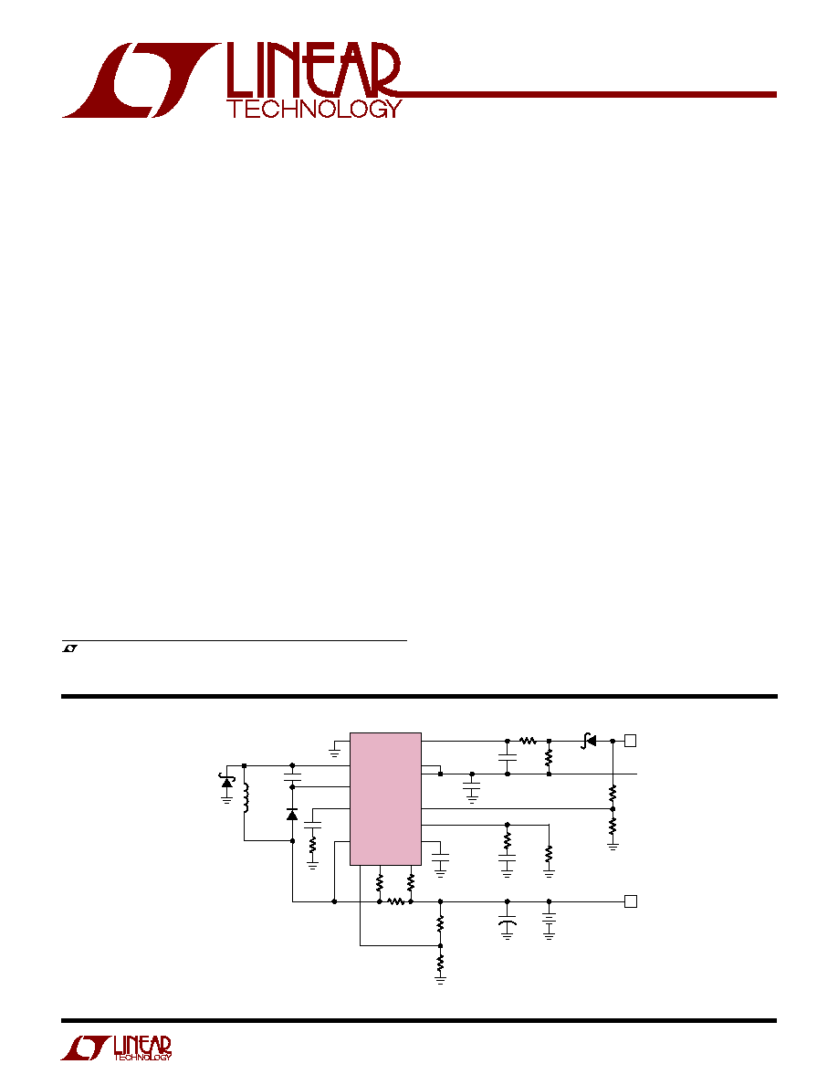
Figure 1. 2A Lithium-Ion Battery Charger
s
Chargers for NiCd, NiMH, Lead-Acid, Lithium
Rechargeable Batteries
s
Switching Regulators with Precision Current Limit
, LTC and LT are registered trademarks of Linear Technology Corporation.
*US patent number 5,723,970
**See LT1510 for 1.5A charger; see LT1511 for 3A charger
FEATURES
DESCRIPTIO
U
APPLICATIO S
U
TYPICAL APPLICATIO
U
SW
BOOST
COMP1
CLN
UV
OVP SENSE
BAT
C1
1
Á
F
R
S4
ADAPTER
CURRENT SENSE
R7
500
R5
UNDERVOLTAGE
LOCKOUT
R6
5k
V
IN
(ADAPTER INPUT)
11V TO 28V
V
BAT
C
PROG
1
Á
F
C
IN
*
15
Á
F
300
R
PROG
4.93k
1%
0.33
Á
F
C2
0.47
Á
F
R
S3
200
1%
R
S2
200
1%
L1**
22
Á
H
D2
1N4148
2nF
10k
R
S1
0.05
BATTERY CURRENT
SENSE
R3
390k
0.25%
BATTERY
VOLTAGE SENSE
R4
162k
0.25%
C
OUT
22
Á
F
TANT
8.4V
Li-Ion
LT1769
NOTE: COMPLETE LITHIUM-ION CHARGER,
NO TERMINATION REQUIRED. R
S4
, R7
AND C1 ARE OPTIONAL FOR I
IN
LIMITING
*TOKIN OR UNITED CHEMI-CON/MARCON
CERAMIC SURFACE MOUNT
**22
Á
H SUMIDA CDRH125
SEE APPLICATIONS INFORMATION FOR
INPUT CURRENT LIMIT AND UNDERVOLTAGE LOCKOUT
GENERAL SEMICONDUCTOR. FOR T
J
LESS THEN 100
░
C
MBRS130LT3 CAN BE USED
V
CC
TO MAIN
SYSTEM LOAD
SPIN
D1
SS24
GND
CLP
D3
SS24
1511 Ě F01
PROG
V
C
+

2
LT1769
ABSOLUTE
M
AXI
M
U
M
RATINGS
W
W
W
U
PACKAGE/ORDER I
N
FOR
M
ATIO
N
W
U
U
ORDER PART
NUMBER
Consult factory for Military grade parts.
*ALL V
CC
PINS SHOULD
BE CONNECTED
TOGETHER CLOSE TO
THE PINS
** ALL GND PINS ARE
FUSED TO INTERNAL DIE
ATTACH PADDLE FOR
HEAT SINKING. CONNECT
THESE PINS TO
EXPANDED PC LANDS
FOR PROPER HEAT
SINKING. 35
░
C/W
THERMAL RESISTANCE
ASSUMES AN INTERNAL
GROUND PLANE
DOUBLING AS A HEAT
SPREADER
LT1769CGN
LT1769IGN
T
JMAX
= 125
░
C,
JA
= 35
░
C/ W**
1
2
3
4
5
6
7
8
9
10
11
12
13
14
TOP VIEW
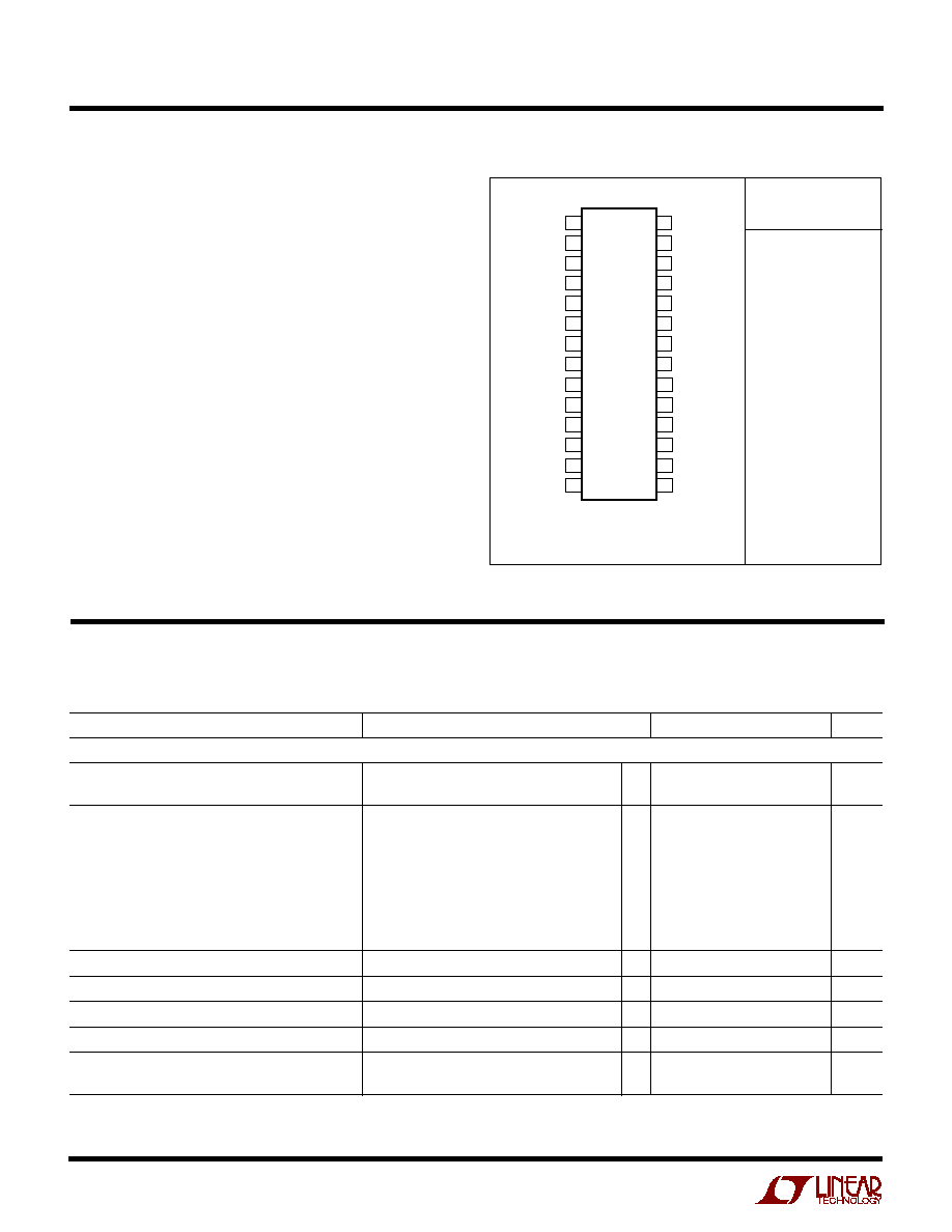
GN PACKAGE
28-LEAD PLASTIC SSOP
28
27
26
25
24
23
22
21
20
19
18
17
16
15
GND**
GND**
GND**
SW
BOOST
UV
GND**
GND**
OVP
CLP
CLN
COMP1
SENSE
GND**
GND**
GND**
GND**
V
CC1
*
V
CC2
*
V
CC3
*
GND**
PROG
V
C
UV
OUT
COMP2
BAT
SPIN
GND**
ELECTRICAL CHARACTERISTICS
(Note 1)
Supply Voltage
(V
CC
, CLP and CLN Pin Voltage) ......................... 30V
BOOST Pin Voltage with Respect to V
CC
................. 25V
I
BAT
(Average) ........................................................... 2A
Operating Junction Temperature Range
Commercial ........................................... 0
░
C to 125
░
C
Industrial ......................................... ş 40
░
C to 125
░
C
Operating Ambient Temperature
Commercial ............................................ 0
░
C to 70
░
C
Industrial ........................................... ş 40
░
C to 85
░
C
Storage Temperature Range ................. ş 65
░
C to 150
░
C
Lead Temperature (Soldering, 10 sec).................. 300
░
C
The
q
denotes specifications which apply over the full operating
temperature range, otherwise specifications are at T
A
= 25
░
C. V
CC
= 16V, V
BAT
= 8V, R
S2
= R
S3
= 200
(see Block Diagram),
V
CLN
= V
CC
. No load on any outputs unless otherwise noted.
PARAMETER
CONDITIONS
MIN
TYP
MAX
UNITS
Overall
Supply Current
V
PROG
= 2.7V, V
CC
20V
q
4.5
6.8
mA
V
PROG
= 2.7V, 20V < V
CC
25V
q
4.6
7.0
mA
Sense Amplifier CA1 Gain and Input Offset Voltage
8V
V
CC
25V , 0V
V
BAT
20V
(With R
S2
= 200
, R
S3
= 200
)
R
PROG
= 4.93k
q
93
100
107
mV
(Measured across R
S1
)(Note 2)
R
PROG
= 49.3k
q
8
10
12
mV
T
A
< 0
░
C
7
12
mV
V
CC
= 28V, V
BAT
= 20V
R
PROG
= 4.93k
q
90
110
mV
R
PROG
= 49.3k
q
6
14
mV
T
A
< 0
░
C
7
13
mV
V
CC
Undervoltage Lockout (Switch OFF) Threshold
Measured at UV Pin
q
6
7
8
V
UV Pin Input Current
0.2V
V
UV
8V
q
0.1
5
Á
A
UV Output Voltage at UV
OUT
Pin
In Undervoltage State, I
UVOUT
= 70
Á
A
q
0.1
0.5
V
UV Output Leakage Current at UV
OUT
Pin
8V
V
UV
, V
UVOUT
= 5V
q
0.1
3
Á
A
Reverse Current from Battery (When V
CC
Is
V
BAT
20V, V
UV
0.4V
3
15
Á
A
Not Connected, V
SW
Is Floating)

3
LT1769
ELECTRICAL CHARACTERISTICS
The
q
denotes specifications which apply over the full operating
temperature range, otherwise specifications are at T
A
= 25
░
C. V
CC
= 16V, V
BAT
= 8V, R
S2
= R
S3
= 200
(see Block Diagram),
V
CLN
= V
CC
. No load on any outputs unless otherwise noted.
PARAMETER
CONDITIONS
MIN
TYP
MAX
UNITS
Overall
Boost Pin Current
V
CC
= 20V, V
BOOST
= 0V
0.1
10
Á
A
V
CC
= 28V, V
BOOST
= 0V
0.25
20
Á
A
2V
V
BOOST
ş V
CC
< 8V (Switch ON)
6
9
mA
8V
V
BOOST
ş V
CC
25V (Switch ON)
8
12
mA
Switch
Switch ON Resistance
8V
V
CC
V
MAX
, I
SW
= 2A,
V
BOOST
ş V
SW
2V
q
0.15
0.25
I
BOOST
/
I
SW
During Switch ON
V
BOOST
= 24V, I
SW
2A
25
35
mA/A
Switch OFF Leakage Current
V
SW
= 0V, V
CC
20V
q
2
100
Á
A
20V < V
CC
28V
q
4
200
Á
A
Minimum I
PROG
for Switch ON
q
2
4
20
Á
A
Minimum I
PROG
for Switch OFF
q
1
2.4
mA
Maximum V
BAT
for Switch ON
q
V
CC
ş 2
V
Current Sense Amplifier CA1 Inputs (Sense, BAT)
Input Bias Current
q
ş 50
ş 125
Á
A
Input Common Mode Low
q
ş 0.25
V
Input Common Mode High
q
V
CC
ş 2
V
SPIN Input Current
ş 100
ş 200
Á
A
Reference
Reference Voltage (Note 3)
R
PROG
= 4.93k, Measured at OVP with
VA Supplying I
PROG
and Switch OFF
2.448
2.465
2.477
V
Reference Voltage
All Conditions of V
CC
, T
A
0
░
C
q
2.441
2.489
V
T
A
< 0
░
C (Note 4)
q
2.43
2.489
V
Oscillator
Switching Frequency
180
200
220
kHz
Switching Frequency
All Conditions of V
CC
, T
A
0
░
C
q
170
200
230
kHz
T
A
< 0
░
C
q
160
230
kHz
Maximum Duty Cycle
90
93
%
q
85
%
Current Amplifier CA2
Transconductance
V
C
= 1V, I
VC
=
▒
1
Á
A
150
250
550
Á
mho
Maximum V
C
for Switch OFF
q
0.6
V
I
VC
Current (Out of Pin)
V
C
0.6V
100
Á
A
V
C
< 0.45V
3
mA

4
LT1769
ELECTRICAL CHARACTERISTICS
TYPICAL PERFOR
M
A
N
CE CHARACTERISTICS
U
W
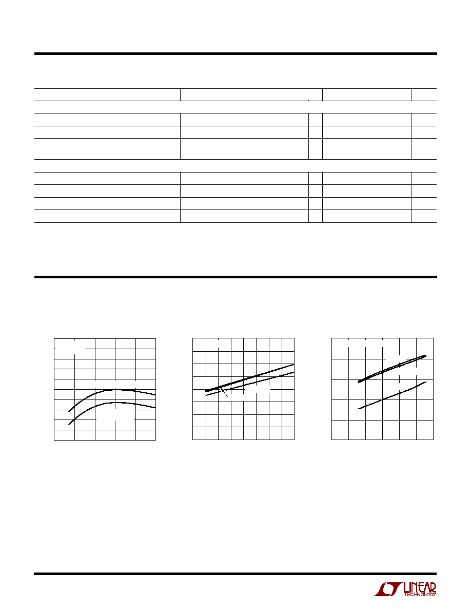
Efficiency of Figure 1 Circuit
I
BAT
(A)
0.2
EFFICIENCY (%)
100
98
96
94
92
90
88
86
84
82
80
1.0
1.8
2.2
1769 G01
0.6
1.4
V
IN
= 16.5
V
BAT
= 8.4V
CHARGER EFFICIENCY
INCLUDES LOSS
IN DIODE D3
V
CC
(V)
0
I
CC
(mA)
7.0
6.5
6.0
5.5
5.0
4.5
5
10
15
20
1769 G03
25
30
T
J
= 125
░
C
T
J
= 25
░
C
T
J
= 0
░
C
MAXIMUM DUTY CYCLE
I
CC
vs Duty Cycle
DUTY CYCLE (%)
0
10
30
50
70
I
CC
(mA)
80
1769 G02
20
40
60
8
7
6
5
4
3
2
1
0
T
J
= 125
░
C
T
J
= 0
░
C
T
J
= 25
░
C
V
CC
= 16V
I
CC
vs V
CC
The
q
denotes specifications which apply over the full operating
temperature range, otherwise specifications are at T
A
= 25
░
C. V
CC
= 16V, V
BAT
= 8V. No load on any outputs unless otherwise noted.
PARAMETER
CONDITIONS
MIN
TYP
MAX
UNITS
Voltage Amplifier VA
Transconductance (Note 3)
Output Current from 50
Á
A to 500
Á
A
0.25
0.6
1.3
mho
Output Source Current
V
OVP
= V
REF
+ 10mV, V
PROG
= V
REF
+ 10mV
1.1
mA
OVP Input Bias Current
VA Output Current at 0.5mA
q
▒
3
▒
10
nA
VA Output Current at 0.5mA, T
A
> 90
░
C
q
ş15
25
nA
Current Limit Amplifier CL1, 8V
Input Common Mode
Turn-On Threshold
0.5mA Output Current
93
100
107
mV
Transconductance
Output Current from 50
Á
A to 500
Á
A
0.5
1
2
mho
CLP Input Current
0.5mA Output Current, V
UV
0.4V
0.3
1
Á
A
CLN Input Current
0.5mA Output Current V
UV
0.4V
0.8
2
mA
Note 1: Absolute Maximum Ratings are those values beyond which the life
of a device may be impaired.
Note 2: Tested with Test Circuit 1.
Note 3: Tested with Test Circuit 2.
Note 4: A linear interpolation can be used for reference voltage
specification between 0
░
C and ş 40
░
C.

5
LT1769
TYPICAL PERFOR
M
A
N
CE CHARACTERISTICS
U
W
V
CC
(V)
0
V
REF
(V)
0.003
0.002
0.001
0
ş0.001
ş0.002
ş0.003
5
10
15
20
1769 G04
25
30
ALL TEMPERATURES
V
REF
Line Regulation
I
VA
vs
V
OVP
(Voltage Amplifier)
I
VA
(mA)
0
V
OVP
(mV)
4
3
2
1
0
0.8
1769 G05
0.2
0.1
0.3
0.5
0.7
0.9
0.4
0.6
1.0
T
J
= 125
░
C
T
J
= 25
░
C
V
C
Pin Characteristics
V
C
(V)
0
0.2
0.6
1.0
1.4
1.8
I
VC
(mA)
ş1.20
ş1.08
ş0.96
ş0.84
ş0.72
ş0.60
ş0.48
ş0.36
ş0.24
ş0.12
0
0.12
1.6
1769 G07
0.4
0.8
1.2
2.0
JUNCTION TEMPERATURE (
░
C)
0
DUTY CYCLE (%)
120
1769 G06
40
80
98
97
96
95
94
93
92
91
90
20
60
100
140
Maximum Duty Cycle
Reference Voltage
vs Temperature
JUNCTION TEMPERATURE
0
REFERENCE VOLTAGE (V)
2.470
2.468
2.466
2.464
2.462
2.460
2.458
25
50
75
100
1769 G09
125
150
V
PROG
(V)
0
1
2
3
5
4
I
PROG
(mA)
6
0
ş 6
1769 G08
T
J
= 125
░
C
T
J
= 25
░
C
PROG Pin Characteristics

6
LT1769
GND (Pins 1 to 3, 7, 8, 14, 15, 22, 26 to 28): Ground Pins.
Must be connected to expanded PC lands for proper heat
sinking. See Applications Information section for details.
SW (Pin 4): Switch Output. The Schottky catch diode must
be placed with very short lead length in close proximity to
SW pin and GND.
BOOST (Pin 5): This pin is used to bootstrap and drive the
switch power NPN transistor to a low on-voltage for low
power dissipation. In Figure 1, V
BOOST
= V
CC
+ V
BAT
when
switch is on. For lowest IC power dissipation, connect
boost diode D1 to a 3V to 6V at 30mA voltage source (see
Figure 10).
UV (Pin 6): Undervoltage Lockout Input. The rising thresh-
old is at 6.7V with a hysteresis of 0.5V. Switching stops in
undervoltage lockout. When the input supply (normally
the wall adapter output) to the IC is removed, the UV pin
must be pulled down to below 0.7V (a 5k resistor from
adapter output to GND is required) otherwise the reverse
battery current drained by the IC will be approximately
200
Á
A instead of 3
Á
A. Do not leave the UV pin floating.
When connected to V
IN
with no resistor divider, the built-
in 6.7V undervoltage lockout will be effective.
OVP (Pin 9): This is the input to amplifier VA with a
threshold of 2.465V. Typical bias current is about 3nA out
of this pin. For charging lithium-ion batteries, VA monitors
the battery voltage and reduces charging when battery
voltage reaches the preset value. If it is not used, the OVP
pin should be grounded.
CLP (Pin 10): This is the positive input to the input current
limit amplifier CL1. The threshold is set at 100mV. When
used to limit supply current, a filter is needed to filter out
the 200kHz switching noise.
CLN (Pin 11): This is the negative input to the input current
limit amplifier CL1.
COMP1 (Pin 12): This is the compensation node for the
input current limit amplifier CL1. At input adapter current
limit, this node rises to 1V. By forcing COMP1 low with an
external transistor, amplifier CL1 will be defeated (no
adapter current limit). COMP1 can source 200
Á
A. If this
function is not used, the resistor and capacitor on COMP1
pin, shown on the Figure 1 circuit, are not needed.
SENSE (Pin 13): Current Amplifier CA1 Input. Sensing can
be at either terminal of the battery.
SPIN (Pin 16): This pin is for the current amplifier CA1
bias. It must be connected to R
S1
as shown in the 2A
Lithium Battery Charger (Figure 1).
BAT (Pin 17): Current Amplifier CA1 Input.
COMP2 (Pin 18): This is also a compensation node for
amplifier CL1. Voltage on this pin rises to 2.8V at input
adapter current limit and/or at constant-voltage charging.
UV
OUT
(Pin 19): This is an open-collector output for
undervoltage lockout status. It stays low in undervoltage
state. With an external pull-up resistor, it goes high at valid
V
CC
. Note that the base drive of the open-collector NPN
comes from CLN pin. UV
OUT
stays low only when CLN is
higher than 2V. Pull-up current should be kept under
100
Á
A.
V
C
(Pin 20): This is the inner loop control signal for the
current mode PWM. Switching starts at 0.7V. In normal
operation, a higher V
C
corresponds to higher charge
current. A capacitor of at least 0.33
Á
F to GND filters out
noise and controls the rate of soft start. To stop switching,
pull this pin low. Typical output current is 30
Á
A.
PROG (Pin 21): This pin is for programming the charge
current and for system loop compensation. During normal
operation, V
PROG
stays close to 2.465V. If it is shorted to
GND switching will stop. When a microprocessor con-
trolled DAC is used to program charge current, it must be
capable of sinking current at a compliance up to 2.465V.
V
CC1
,
V
CC2
,
V
CC3
(Pins 23 to 25): Input Supply. For good
bypass, a low ESR capacitor of 15
Á
F or higher is required,
with the lead length kept to a minimum. V
CC
should be
between 8V and 28V and at least 3V higher than V
BAT
.
Undervoltage lockout starts and switching stops when
V
CC
goes below 7V typical. Note that there is an internal
parasitic diode from SW pin to V
CC
pin. Do not force V
CC
below SW by more than 0.7V with battery present. All three
V
CC
pins should be shorted together close to the pins.
PI
N
FU
N
CTIO
N
S
U
U
U

7
LT1769
BLOCK DIAGRA
M
W
ş
+
ş
+
ş
+
ş
+
ş
+
V
SW
0.7V
1.5V
V
BAT
V
REF
V
C
GND
UV
SLOPE COMPENSATION
R2
R3
C1
PWM
B1
CA2
ş
+
ş
+
CA1
VA
+
+
ş
+
7V
+
V
REF
2.465V
SHUTDOWN
200kHz
OSCILLATOR
S
R
R
R
R1
1k
R
PROG
V
CC
UV
OUT
V
CC
BOOST
SW
SENSE
SPIN
BAT
I
PROG
R
S3
R
S2
R
S1
I
BAT
0VP
BAT
1769 BD
PROG
I
PROG
I
BAT
=
(I
PROG
)(R
S2
)
R
S1
C
PROG
75k
Q
SW
V
CC
g
m
= 0.64
ş
+
CL1
CLP
100mV
CLN
COMP1
COMP2
+
=
(R
S3
= R
S2
)
2.465V
R
PROG
R
S2
R
S1
( () )

8
LT1769
TEST CIRCUITS
Test Circuit 1
ş
+
V
REF
0.65V
V
BAT
V
C
CA2
ş
+
ş
+
CA1
+
300
20k
1k
1k
R
S1
100
BAT
SENSE
SPIN
1769 TC01
PROG
R
PROG
0.047
Á
F
LT1769
1
Á
F
60k
LT1006
+
R
S2
200
R
S3
200
Test Circuit 2
V
REF
2.465V
ş
+
+
10k
10k
OVP
1769 TC02
I
PROG
R
PROG
LT1769
PROG
LT1013
0.47
Á
F
ş
+
VA
OPERATIO
N
U
The LT1769 is a current mode PWM step-down (buck)
switcher. The battery DC charge current is programmed
by a resistor R
PROG
(or a DAC output current) at the PROG
pin (see Block Diagram). Amplifier CA1 converts the
charge current through R
S1
to a much lower current I
PROG
fed into the PROG pin. Amplifier CA2 compares the output
of CA1 with the programmed current and drives the PWM
control loop to force them to be equal. High DC accuracy
is achieved with averaging capacitor C
PROG
. Note that
I
PROG
has both AC and DC components. I
PROG
goes
through R1 and generates a ramp signal that is fed to the
PWM control comparator C1 through buffer B1 and level
shift resistors R2 and R3, forming the current mode inner
loop. The BOOST pin drives the switch NPN Q
SW
into
saturation and reduces power loss. For batteries like
lithium-ion that require both constant-current and con-
stant-voltage charging, the 0.5%, 2.465V reference and
the amplifier VA reduce the charge current when battery
voltage reaches the preset level. For NiMH and NiCd, VA
can be used for overvoltage protection. When the input
voltage is removed, the V
CC
pin drops to 0.7V below the
battery voltage, forcing the charger into a low battery drain
(3
Á
A typical) sleep mode. To shut down the charger,
simply pull the V
C
pin low with a transistor.

9
LT1769
APPLICATIO
N
S I
N
FOR
M
ATIO
N
W
U
U
U
Input and Output Capacitors
In the 2A Lithium-Ion Battery Charger (Figure 1), the input
capacitor (C
IN
) is assumed to absorb all input switching
ripple current in the converter, so it must have adequate
ripple current rating. Worst-case RMS ripple current will
be equal to one half of the output charge current. Actual
capacitance value is not critical. Solid tantalum capacitors
such as the AVX TPS and Sprague 593D series have high
ripple current rating in a relatively small surface mount
package, but
caution must be used when tantalum capaci-
tors are used for input bypass. High input surge currents
are possible when the adapter is hot-plugged to the
charger and solid tantalum capacitors have a known
failure mechanism when subjected to very high turn-on
surge currents. Selecting a high voltage rating on the
capacitor will minimize problems. Consult with the manu-
facturer before use. Alternatives include new high capacity
ceramic (5
Á
F to 20
Á
F) from Tokin or United Chemi-Con/
Marcon, et al. Sanyo OS-CON can also be used.
The output capacitor (C
OUT
) is also assumed to absorb
output switching ripple current. The general formula for
capacitor ripple current is:
I
RMS
=
(L1)(f)
V
BAT
V
CC
( )
0.29 (V
BAT
) 1 ş
For example, V
CC
= 16V, V
BAT
= 8.4V, L1 = 20
Á
H,
and f = 200kHz, I
RMS
= 0.3A.
EMI considerations usually make it desirable to minimize
ripple current in the battery leads. Beads or inductors can
be added to increase battery impedance at the 200kHz
switching frequency. Switching ripple current splits be-
tween the battery and the output capacitor depending on
the ESR of the output capacitor and the battery imped-
ance. If the ESR of C
OUT
is 0.2
and the battery impedance
is raised to 4
with a bead or inductor, only 5% of the
ripple current will flow into the battery.
Soft-Start and Undervoltage Lockout
The LT1769 is soft-started by the 0.33
Á
F capacitor on the
V
C
pin. On start-up, the V
C
pin voltage will quickly rise to
0.5V, then ramp at a rate set by the internal 45
Á
A pull-up
current and the external capacitor. Charge current starts
ramping up when V
C
pin voltage reaches 0.7V and full
current is achieved with V
C
at 1.1V. With a 0.33
Á
F capaci-
tor, the time to reach full charge current is about 10ms and
it is assumed that input voltage to the charger will reach
full value in less than 10ms. The capacitor can be
increased up to 1
Á
F if longer input start-up times are
needed.
In any switching regulator, conventional time-based soft-
starting can be defeated if the input voltage rises much
slower than the time out period. This happens because the
switching regulators in the battery charger and the com-
puter power supply are typically supplying a fixed amount
of power to the load. If the input voltage comes up slowly
compared to the soft-start time, the regulators will try to
deliver full power to the load when the input voltage is still
well below its final value. If the adapter is current limited,
it cannot deliver full power at reduced output voltages and
the possibility exists for a quasi "latch" state where the
adapter output stays in a current limited state at reduced
output voltage. For instance, if maximum charger plus
computer load power is 25W, a 15V adapter might be
current limited at 2A. If adapter voltage is less than
(25W/2A = 12.5V) when full power is drawn, the adapter
voltage will be pulled down by the constant 25W load until
it reaches a lower stable state where the switching regu-
lators can no longer supply full load. This situation can be
prevented by utilizing
undervoltage lockout, set higher
than the minimum adapter voltage where full power can be
achieved.
A fixed undervoltage lockout of 7V is built into the LT1769.
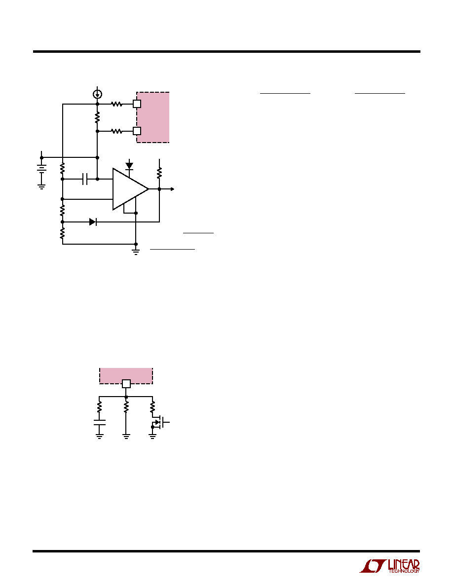
This 7V threshold can be increased by adding a resistive
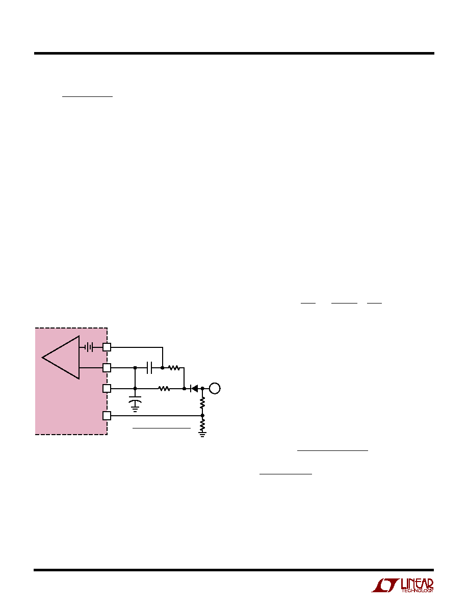
divider to the UV pin as shown in Figure 2. Internal lockout
is performed by clamping the V
C
pin low. The V
C
pin is
released from its clamped state when the UV pin rises
above 7V and is pulled low when the UV pin drops below
6.5V (0.5V hysteresis). At the same time UV
OUT
goes high
with an external pull-up resistor. This signal can be used
to alert the system that charging is about to start. The
charger will start delivering current about 4ms after V
C
is
released, as set by the 0.33
Á
F capacitor. A resistor divider
is used to set the desired V
CC
lockout voltage as shown in
Figure 2. A typical value for R6 is 5k and R5 is found from:

10
LT1769
APPLICATIO
N
S I
N
FOR
M
ATIO
N
W
U
U
U
R5 =
R6(V
ş V
)
V
UV
UV
IN
V
UV
= Rising lockout threshold on the UV pin
V
IN
= Charger input voltage that will sustain full load power
Example: With R6 = 5k, V
UV
= 6.7V and setting V
IN
at 12V;
R5 = 5k (12V ş 6.7V)/6.7V = 4k
The resistor divider should be connected directly to the
adapter output as shown, not to the V
CC
pin, to prevent
battery drain with no adapter voltage. If the UV pin is not
used, connect it to the adapter output (not V
CC
) and
connect a resistor no greater than 5k to ground. Floating
this pin will cause reverse battery current to increase from
3
Á
A to 200
Á
A.
If connecting the unused UV pin to the adapter output is
not possible, it can be grounded. Although it would seem
that grounding the pin creates a permanent lockout state,
the UV circuitry is arranged for phase reversal with low
voltages on the UV pin to allow the grounding technique to
work.
ally, batteries will automatically be charged at the maximum
possible rate of which the adapter is capable.
This is accomplished by sensing total adapter output
current and adjusting the charge current downward if a
preset adapter current limit is exceeded. True analog
control is used, with closed-loop feedback ensuring that
adapter load current remains below the limit. Amplifier
CL1 in Figure 2 senses the voltage across R
S4
, connected
between the CLP and CLN pins. When this voltage exceeds
100mV, the amplifier will override the programmed charge
current to limit adapter current to 100mV/R
S4
. A lowpass
filter formed by 500
and 1
Á
F is required to eliminate
switching noise. If the input current limit is not used, both
CLP and CLN pins should be connected to V
CC
.
Charge Current Programming
The basic formula for charge current is (see Block
Diagram):
I
BAT
= I
PROG
=
2.465V
R
PROG
R
S2
R
S1
( )( )
R
S2
R
S1
( )
where R
PROG
is the total resistance from PROG pin to ground.
For the sense amplifier CA1 biasing purpose, R
S3
should
have the same value as R
S2
and SPIN should be connected
directly to the sense resistor (R
S1
) as shown in the Block
Diagram.
For example, 2A charge current is needed. For low power
dissipation on R
S1
and enough signal to drive the amplifier
CA1, let R
S1
= 100mV/2A = 0.05
. This limits R
S1
power
to 0.2W. Let R
PROG
= 5k, then:
R
S2
= R
S3
=
=
= 200
(I
BAT
)(R
PROG
)(R
S1
)
2.465V
(2A)(5k)(0.05)
2.465V
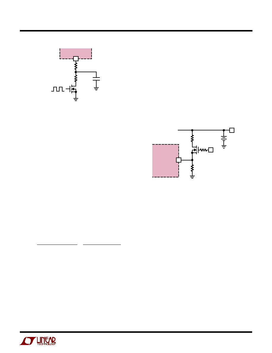
Charge current can also be programmed by pulse width
modulating I
PROG
with a switch Q1 to R
PROG
at a frequency
higher than a few kHz (Figure 3). Charge current will be
proportional to the duty cycle of the switch with full current
at 100% duty cycle.
100mV
500
CLP
CLN
V
CC
UV
1769 F02
R5
LT1769
R6
1
Á
F
+
R
S4
*
V
IN
AC ADAPTER
OUTPUT
*R
S4
=
100mV
ADAPTER CURRENT LIMIT
+
ş
+
CL1
Figure 2. Adapter Input Current Limiting
Adapter Current Limiting
An important feature of the LT1769 is the ability to
automatically adjust charge current to a level which avoids
overloading the wall adapter. This allows the product to
operate at the same time the batteries are being charged
without complex load management algorithms. Addition-

11
LT1769
APPLICATIO
N
S I
N
FOR
M
ATIO
N
W
U
U
U
When power is on, there is about 200
Á
A of current flowing
out of the BAT and SENSE pins. If the battery is removed
during charging, and total load including R3 and R4 is less
than 200
Á
A, V
BAT
could float up to V
CC
even though the
loop has turned switching off. To keep V
BAT
regulated to
the battery voltage in this condition, R3 and R4 can be
chosen to draw 0.5mA and Q3 can be added to disconnect
them when power is off (Figure 4). R5 isolates the OVP pin
from any high frequency noise on V
IN
. An alternative method
is to use a Zener diode with a breakdown voltage two or three
volts higher than battery voltage to clamp the V
BAT
voltage.
Lithium-Ion Charging
The 2A Lithium-Ion Battery Charger (Figure 1) charges at
a constant 2A until battery voltage reaches a limit set by R3
and R4. The charger will then automatically go into a
constant-voltage mode with current decreasing to near
zero over time as the battery reaches full charge. This is the
normal regimen for lithium-ion charging, with the charger
holding the battery at "float" voltage indefinitely. In this
case no external sensing of full charge is needed.
Battery Voltage Sense Resistors Selection
To minimize battery drain when the charger is off, current
through the R3/R4 divider is set at 15
Á
A. The input current
to the OVP pin is 3nA and the error can be neglected.
With divider current set at 15
Á
A, V
BAT
= 8.4V, R4 =
2.465/15
Á
A = 162k and,
R3
R4 V
2.465
2.465
162k 8.4 2.465
2.465
390k
BAT
=
( )
-
(
)
=
-
(
)
=
Li-Ion batteries typically require float voltage accuracy of
1% to 2%. Accuracy of the LT1769 OVP voltage is
▒
0.5%
at 25
░
C and
▒
1% over full temperature. This leads to the
possibility that very accurate (0.1%) resistors might be
needed for R3 and R4. Actually, the temperature of the
LT1769 will rarely exceed 50
░
C in float mode because
charging currents have tapered off to a low level, so 0.25%
resistors will normally provide the required level of overall
accuracy.
Figure 4. Disconnecting Voltage Divider
PWM
R
PROG
4.7k
300
PROG
C
PROG
1
Á
F
Q1
VN2222
5V
0V
LT1769
1769 F03
I
BAT
= (DC)(2A)
Figure 3. PWM Current Programming
R3
12k
0.25%
R4
4.99k
0.25%
OVP
V
IN
+
8.4V
V
BAT
Q3
VN2222
LT1769
1769 F04
R5
220k
Some battery manufacturers recommend terminating the
constant-voltage float mode after charge current has
dropped below a specified level (typically around 10% of
the full current)
and a further time out period of 30 to 90
minutes has elapsed. This may extend battery life, so
check with the manufacturer for details. The circuit in
Figure 5 will detect when charge current has dropped
below 270mA. This logic signal is used to initiate a timeout
period, after which the LT1769 can be shut down by
pulling the V
C
pin low with an open collector or drain.
Some external means must be used to detect the need for
additional charging or the charger may be turned on
periodically to complete a short float-voltage cycle.
Current trip level is determined by the battery voltage, R1
through R3 and the sense resistor (R
S1
). D2 generates
hysteresis in the trip level to avoid multiple comparator
transitions.

12
LT1769
APPLICATIO
N
S I
N
FOR
M
ATIO
N
W
U
U
U
Figure 5. Current Comparator for Initiating Float Time Out
NEGATIVE EDGE
TO TIMER
1769 F04
3.3V OR 5V
ADAPTER
OUTPUT
3
8
7
1
4
2
D1
1N4148
C1
0.1
Á
F
BAT
SENSE
R1*
1.6k
R
S1
0.05
R4
470k
R3
430k
R2
560k
LT1011
D2
1N4148
* TRIP CURRENT =
=
270mA
R1(V
BAT
)
(R2 + R3)(R
S1
)
(1.6k)(8.4V)
(560k + 430k)(0.05
)
+
ş
V
BAT
BAT
R
S3
200
R
S2
200
LT1769
I
BAT
R1
2.465 2000
I
R2
2.465 2000
I
I
LOW
HI
LOW
=
( )( )
=
( )( )
-
All battery chargers with fast charge rates require some
means to detect full charge in the battery and terminate the
high charge current. NiCd batteries are typically charged at
high current until a temperature rise or battery voltage
decrease is detected as an indication of near full charge.
The charging current is then reduced to a much lower
value and maintained as a constant trickle charge. An
intermediate "top off" current may also be used for a fixed
time period to reduce total charge time.
NiMH batteries are similar in chemistry to NiCd but have
two differences related to charging. First, the inflection
characteristic in battery voltage as full charge is approached
is not nearly as pronounced. This makes it more difficult
to use ş dV/dt as an indicator of full charge, and an
increase in battery temperature is more often used with a
temperature sensor in the battery pack. Secondly, con-
stant trickle charge may not be recommended. Instead, a
moderate level of current is used on a pulse basis (
1%
to 5% duty cycle) with the time-averaged value substitut-
ing for a constant low trickle. Please contact the Linear
Technology Applications department about charge termi-
nation circuits.
If overvoltage protection is needed, R3 and R4 can be cal-
culated according to the procedure described in Lithium-
Ion Charging section. The OVP pin should be grounded if
not used.
When a microprocessor DAC output is used to control
charge current, it must be capable of sinking current at a
compliance up to 2.5V if connected directly to the PROG pin.
Thermal Calculations
If the LT1769 is used for charging currents above 1A, a
thermal calculation should be done to ensure that junction
temperature will not exceed 125
░
C. Power dissipation in
the IC is caused by bias and driver current, switch resis-
tance and switch transition losses. The GN package, with
a thermal resistance of 35
░
C/W, can provide a full 2A
charging current in many situations. A graph is shown in
the Typical Performance Characteristics section.
For 1A full current, the current sense resistor (R
S1
) should
be increased to 0.1
so that enough signal (10mV) will be
across R
S1
at 0.1A trickle charge to keep charging current
accurate.
For a 2-level charger, R1 and R2 are found from:
Nickel-Cadmium and Nickel-Metal-Hydride Charging
The 2A Lithium-Ion Battery Charger shown in Figure 1 can
be modified to charge NiCd or NiMH batteries. For ex-
ample, if a 2-level charge is needed; 1A when Q1 is on and
100mA when Q1 is off.
Figure 6. 2-Level Charging
R2
5.49k
R1
49.3k
300
PROG
1
Á
F
Q1
LT1769
1769 F05

13
LT1769
APPLICATIO
N
S I
N
FOR
M
ATIO
N
W
U
U
U
Figure 7. Lower V
BOOST
For example, V
X
= 3.3V then:
Then P
DRIVER
=
( )(
)( )
+
( )
I
V
V
V
V
BAT
BAT
X
X
IN
1
30
55
Total Power in the IC is: 0.35 + 0.43 + 0.5 = 1.3W
Temperature rise will be (1.3W)(35
░
C/W) = 46
░
C. This
assumes that the LT1769 is properly heat sunk by con-
necting the eleven fused ground pins to expanded traces
and that the PC board has a backside or internal plane for
heat spreading.
The P
DRIVER
term can be reduced by connecting the boost
diode D2 (see Figure 7) to a lower system voltage (lower
than V
BAT
) instead of V
BAT
.
SW
BOOST
SPIN
1769 F07
LT1769
V
X
I
VX
C2
D2
10
Á
F
L1
+
P
A
V
V
V
V
W
DRIVER
=
( )( )( )
+
( )
=
2
12 6
3 3
1
3 3
30
55 19
0 09
.
.
.
.
The average I
VX
required is:
P
V
W
V
mA
DRIVER
X
=
=
0 09
3 3
28
.
.
The previous example shows the dramatic drop in driver
power dissipation when the boost diode (D2) is connected
to an external 3.3V source instead of the 12.6V battery.
P
DRIVER
drops from 0.43W to 0.09W resulting in an
approximately 12
░
C drop in junction temperature.
Fused-lead packages conduct most of their heat out the
leads. This makes it very important to provide as much PC
board copper around the leads as is practical. Total
thermal resistance of the package-board combination is
dominated by the characteristics of the board in the
immediate area of the package. This means both lateral
thermal resistance across the board and vertical thermal
resistance through the board to other copper layers. Each
layer acts as a thermal heat spreader that increases the
heat sinking effectiveness of extended areas of the board.
Total board area becomes an important factor when the
area of the board drops below about 20 square inches. The
graph in Figure 8 shows thermal resistance vs board area
for 2-layer and 4-layer boards with continuous copper
planes. Note that 4-layer boards have significantly lower
thermal resistance, but both types show a rapid increase
for reduced board areas. Figure 9 shows actual measured
lead temperatures for chargers operating at full current.
P
3.5mA V
1.5mA V
V
V
7.5mA
0.012 I
P
I
V
55 V
P
I
R
V
V
t
V
I
f
BIAS
IN
BAT
BAT
2
IN
BAT
DRIVER
BAT
BAT
2
IN
SW
BAT
2
SW
BAT
IN
OL
IN
BAT
=
(
)( )
+
(
)
+
(
)
+
(
)( )
[
]
=
( )(
)
+
( )
=
( ) ( )(
)
+
( )( )( )( )
1
30
V
BAT
P
3.5mA 19
1.5mA 12.6
12.6
19
7.5mA
0.012 2000mA
0.35W
P
2 12.6
55 19
0.43W
P
2
0.16 12.6
19
10
19 2 200kHz
0.42 0.08
0.5W
BIAS
2
DRIVER
2
SW
2
9
=
(
)( )
+
( )
+
( )
+
( )(
)
[
]
=
=
( )( )
+
( )
=
=
( ) ( )( )
+
( )( )(
)
=
+
=
-
1
12 6
30
.
R
SW
= Switch ON resistance
0.16
t
OL
= Effective switch overlap time
10ns
f = 200kHz
Example: V
IN
= 19V, V
BAT
= 12.6V, I
BAT
= 2A:

14
LT1769
APPLICATIO
N
S I
N
FOR
M
ATIO
N
W
U
U
U
Figure 11. Replacing the Input Diode
CHARGE CURRENT (A)
0
LEAD TEMPERATURE ON PINS 1, 2, 3 (
░
C)
40
50
2
1769 F09
30
20
0.5
1
1.5
70
60
NOTE: PEAK DIE TEMPERATURE
WILL BE ABOUT 15
░
C HIGHER AT
2A CHARGE CURRENT
V
IN
= 19V
V
BAT
= 12.3V
V
BOOST
= 5V
2-LAYER BOARD
ROOM TEMP = 24
░
C
5 IN
2
BOARD
25 IN
2
BOARD
BOARD AREA (IN
2
)
0
45
40
35
30
25
20
15
10
15
25
1769 F08
5
10
20
30
35
THERMAL RESISTANCE (
░
C/
W)
MEASURED FROM AIR AMBIENT
TO DIE USING COPPER LANDS
AS SHOWN ON DATA SHEET
2-LAYER BOARD
4-LAYER BOARD
Figure 8. LT1769 Thermal Resistance
Figure 10. High Duty Cycle
V
IN
SW
BOOST
SPIN
SENSE
BAT
V
CC
V
X
3V TO 6V
C
X
10
Á
F
V
BAT
1769 F11
C2
0.47
Á
F
D2
D1
R
X
50k
Q2
Q1
LT1769
HIGH DUTY CYCLE CONNECTION
Q1 = Si4435DY
Q2 = TP0610L
+
+
SW
BOOST
SPIN
SENSE
BAT
V
BAT
C3
0.47
Á
F
D2
LT1769
SW
BOOST
SPIN
SENSE
BAT
V
X
3V TO 6V
C
X
10
Á
F
V
BAT
1769 F10
C3
0.47
Á
F
D2
LT1769
STANDARD CONNECTION
HIGH DUTY CYCLE CONNECTION
+
+
Battery voltage and input voltage will affect device power
dissipation, so the data sheet power calculations must be
used to extrapolate these readings to other situations.
Vias should be used to connect board layers together.
Planes under the charger area can be cut away from the
rest of the board and connected with vias to form both a
low thermal resistance system and to act as a ground
plane for reduced EMI.
Glue-on, chip-mounted heat sinks are effective only in
moderate power applications where the PC board copper
cannot be used, or where the board size is small. They
offer very little improvement in a properly laid out multi-
layer board of reasonable size.
Higher Duty Cycle for the LT1769 Battery Charger
Maximum duty cycle for the LT1769 is typically 90%, but
this may be too low for some applications. For example, if
an 18V
▒
3% adapter is used to charge ten NiMH cells, the
charger must put out approximaly 15V. A total of 1.6V is
lost in the input diode, switch resistance, inductor resis-
tance and parasitics, so the required duty cycle is
15/16.4 = 91.4%. The duty cycle can be extended to 93%
by restricting boost voltage to 5V instead of using V
BAT
as
is normally done. This lower boost voltage also reduces
power dissipation in the LT1769, so it is a win-win deci-
sion. Connect an external source of 3V to 6V at V
X
node in
Figure 10 with a 10
Á
F C
X
bypass capacitor.
Figure 9. LT1769 Lead Temperature

15
LT1769
APPLICATIO
N
S I
N
FOR
M
ATIO
N
W
U
U
U
Lower Dropout Voltage
For even lower dropout and/or reducing heat on the board,
the input diode D3 can be replaced with a FET (see Figure
11). Connect a P-channel FET in place of the input diode
with its gate connected to the battery causing the FET to
turn off when the input voltage goes low. The problem is
that the gate must be pumped low so that the FET is fully
turned on even when the input is only a volt or two above
the battery voltage. Also there is a turn-off speed issue.
The FET should turn off instantly when the input is dead
shorted to avoid large current surges from the battery
back through the charger into the FET. Gate capacitance
slows turn-off, so a small P-channel (Q2) is added to
discharge the gate capacitance quickly in the event of an
input short. The Q2 body diode creates the necessary
pumping action to keep the gate of Q1 low during normal
operation. Note that Q1 and Q2 have a V
GS
spec limit of
20V. This restricts V
IN
to a maximum of 20V. For low
dropout operation with V
IN
> 20V consult factory.
Optional Diode Connections
The typical application in Figure 1 shows a single diode
(D3) to isolate the V
CC
pin from the adaptor input and to
block reverse input voltage (both steady state and tran-
sient). This simple connection may be unacceptable in
situations where the system load must be powered from
the battery when the adapter input power is removed. As
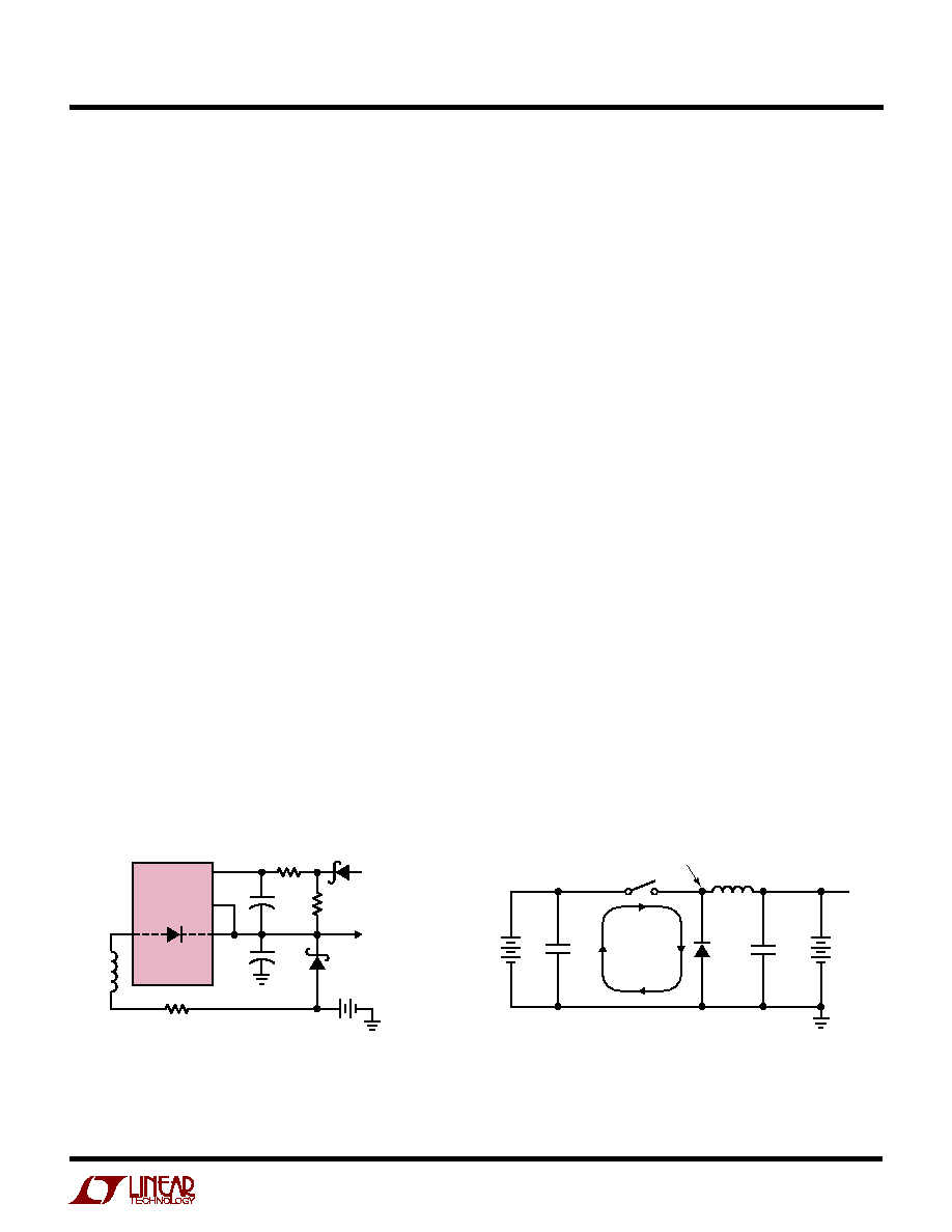
shown in Figure 12, a parasitic diode exists from the SW
pin to the V
CC
pin in the LT1769. When the input power is
removed, this diode will become forward biased and will
provide a current path from the battery to the system load.
Because of diode power limitations, it is not recom-
mended to power the system load through the internal
parasitic diode. To safely power the system load from the
battery, an additional Schottky diode (D4) is needed. For
minimum losses, D4 could be replaced by a low R
DS(ON)
MOSFET which is turned on when the adapter power is
removed.
Layout Considerations
Switch rise and fall times are under 10ns for maximum
efficiency. To minimize radiation, the catch diode, SW pin
and input bypass capacitor leads should be kept as short
as possible. A ground plane should be used under the
switching circuitry to prevent interplane coupling and to
act as a thermal spreading path. All ground pins should be
connected to expanded traces for low thermal resistance.
The fast-switching high current ground path, including the
switch, catch diode and input capacitor, should be kept
very short. Catch diode and input capacitor should be
close to the chip and terminated to the same point. This
path contains nanosecond rise and fall times with several
amps of current. The other paths contain only DC and/or
200kHz tri-wave and are less critical. Figure 13 indicates
the high speed, high current switching path. Figure 14
shows critical path layout. Contact Linear Technology for
the LT1769 circuit PCB layout or Gerber file.
SW
L1
CLP
CLN
ADAPTER
IN
TO
SYSTEM
LOAD
R
S1
C
IN
R
S4
R7
500
C1
1
Á
F
D3
LT1769
INTERNAL
PARASITIC
DIODE
V
CC
1769 F12a
D4
+
+
+
Figure 12. Modified Diode Connection
Figure 13. High Speed Switching Path
1769 F13
V
BAT
L1
V
IN
HIGH
FREQUENCY
CIRCULATING
PATH
BAT
SWITCH NODE
C
IN
C
OUT
D1
Information furnished by Linear Technology Corporation is believed to be accurate and reliable.
However, no responsibility is assumed for its use. Linear Technology Corporation makes no represen-
tation that the interconnection of its circuits as described herein will not infringe on existing patent rights.

16
LT1769
1769f LT/TP 0999 4K Ě PRINTED IN USA
ę
LINEAR TECHNOLOGY CORPORATION 1999
APPLICATIO
N
S I
N
FOR
M
ATIO
N
W
U
U
U
C
IN
C
OUT
R
S1
D1
L1
GND
GND
1769 F14
TO
GND
TO
GND
NOTE: CONNECT ALL GND PINS TO EXPANDED PC LANDS FOR PROPER HEAT SINKING
GND
GND
GND
SW
BOOST
UV
GND
GND
OVP
CLP
CLN
COMP1
SENSE
GND
GND
GND
GND
V
CC1
V
CC2
V
CC3
GND
PROG
V
C
UV
OUT
COMP2
BAT
SPIN
GND
Figure 14. Critical Electrical and Thermal Path Layout
Linear Technology Corporation
1630 McCarthy Blvd., Milpitas, CA 95035-7417
(408) 432-1900
q
FAX: (408) 434-0507
q
www.linear-tech.com
PART NUMBER
DESCRIPTION
COMMENTS
LTC
«
1325
Microprocessor-Controlled Battery Management System
Can Charge, Discharge and Gas Gauge NiCd and Lead-Acid
Batteries with Software Charging Profiles
LT1372/LT1377
500kHz/1MHz Step-Up Switching Regulators
High Frequency, Small Inductor, High Efficiency Switchers, 1.5A Switch
LT1376
500kHz Step-Down Switching Regulator
High Frequency, Small Inductor, High Efficiency Switcher, 1.5A Switch
LT1505
High Current, High Efficiency Battery Charger
94% Efficiency, Synchronous Current Mode PWM
LT1510
Constant-Voltage/Constant-Current Battery Charger
Up to 1.5A Charge Current for Lithium-Ion, NiCd and NiMH Batteries
LT1511
Constant-Voltage/Constant-Current Battery Charger
Up to 3A Charge Current for Lithium-Ion, NiCd and NiMH Batteries
LT1512/LT1513
SEPIC Battery Chargers
V
IN
Can Be Higher or Lower Than Battery Voltage
LTC1729
Li-Ion Battery Charger Termination Controller
Preconditioning If Cell < 2.7V, 3hr Time-Out, C/10 Detection, Temp Sensor
Pin, Charger and Battery Detection
LTC1759
SMBus Smart Battery Charger
94% Efficiency with Input Current Limiting, Up to 8A I
CHG
RELATED PARTS
Dimensions in inches (millimeters) unless otherwise noted.
PACKAGE DESCRIPTIO
N
U
GN Package
28-Lead Plastic SSOP (Narrow 0.150)
(LTC DWG # 05-08-1641)
GN28 (SSOP) 1098
* DIMENSION DOES NOT INCLUDE MOLD FLASH. MOLD FLASH
SHALL NOT EXCEED 0.006" (0.152mm) PER SIDE
** DIMENSION DOES NOT INCLUDE INTERLEAD FLASH. INTERLEAD
FLASH SHALL NOT EXCEED 0.010" (0.254mm) PER SIDE
0.016 ş 0.050
(0.406 ş 1.270)
0.015
▒
0.004
(0.38
▒
0.10)
Î
45
░
0
░
ş 8
░
TYP
0.0075 ş 0.0098
(0.191 ş 0.249)
0.053 ş 0.069
(1.351 ş 1.748)
0.008 ş 0.012
(0.203 ş 0.305)
0.004 ş 0.009
(0.102 ş 0.249)
0.0250
(0.635)
BSC
0.386 ş 0.393*
(9.804 ş 9.982)
1
2
3
4
5
6
7
8
9 10 11 12
0.229 ş 0.244
(5.817 ş 6.198)
0.150 ş 0.157**
(3.810 ş 3.988)
20
21
22
23
24
25
26
27
28
19 18 17
13 14
1615
0.033
(0.838)
REF
