
1
LT1585A/LT1585A-3.3
5A Low Dropout
Fast Response
Positive Regulators
Adjustable and Fixed
The LT
«
1585A/LT1585A-3.3 are low dropout 3-terminal
regulators with 5A output current capability. Design has
been optimized for low voltage applications where tran-
sient response and minimum input voltage are critical.
Similar to the LT1084 family, these regulators feature
lower dropout voltage and faster transient response.
These improvements make them ideal for low voltage
microprocessor applications requiring a regulated 2.5V to
3.6V output with an input supply below 7V.
Current limit is trimmed to ensure specified output current
and controlled short-circuit current. On-chip thermal lim-
iting provides protection against any combination of over-
load that would create excessive junction temperatures.
The LT1585A/LT1585A-3.3 are available in the industry
standard 3-pin TO-220 power package.
DESCRIPTIO
N
U
APPLICATIO
N
S
U
s
Fast Transient Response
s
Guaranteed Dropout Voltage at Multiple Currents
s
Load Regulation: 0.05% Typ
s
Trimmed Current Limit
s
On-Chip Thermal Limiting
s
Standard 3-Pin Power Package
FEATURES
s
Pentium
«
Processor Supplies
s
PowerPC
TM
Supplies
s
Other 2.5V to 3.6V Microprocessor Supplies
s
Low Voltage Logic Supplies
s
Battery-Powered Circuitry
s
Post Regulator for Switching Supply
LT1585ACT
Adjustable
LT1585ACT-3.3
3.3V Fixed
, LTC and LT are registered trademarks of Linear Technology Corporation.
Pentium is a registered trademark of Intel Corporation. PowerPC is a trademark of IBM Corporation.
TYPICAL APPLICATIO
N
U
NOTE: MICROPROCESSOR APPLICATIONS WITH LOAD TRANSIENTS OF 3.8A REQUIRE
OUTPUT DECOUPLING CAPACITANCE >1300
Á
F ON FIXED VOLTAGE PARTS TO ACHIEVE
< 50mV OF DEVIATION FROM NOMINAL OUTPUT. CONSULT FACTORY FOR DETAILS
Dropout Voltage vs Output Current
3.3V, 5A Regulator
LT1585A-3.3
V
IN
4.75V
1585A TA01
C1
10
Á
F
* REQUIRED FOR STABILITY
3.3V
5A
+
C2*
10
Á
F
+
OUTPUT CURRENT (A)
0
INPUT/OUTPUT DIFFERENTIAL (V)
1.5
1.4
1.3
1.2
1.1
1.0
0.9
0.8
0.7
0.6
0.5
LT1585A TA02
I
FULL LOAD
2
LT1585A/LT1585A-3.3
ABSOLUTE
M
AXI
M
U
M
RATINGS
W
W
W
U
V
IN
............................................................................. 7V
Operating Junction Temperature Range
Control Section.................................... 0
░
C to 125
░
C
Power Transistor ................................. 0
░
C to 150
░
C
Storage Temperature Range ................. ş 65
░
C to 150
░
C
Lead Temperature (Soldering, 10 sec) .................. 300
░
C
100% Thermal Limit Functional Test
PRECO
N
DITIO
N
I G
U
U
U
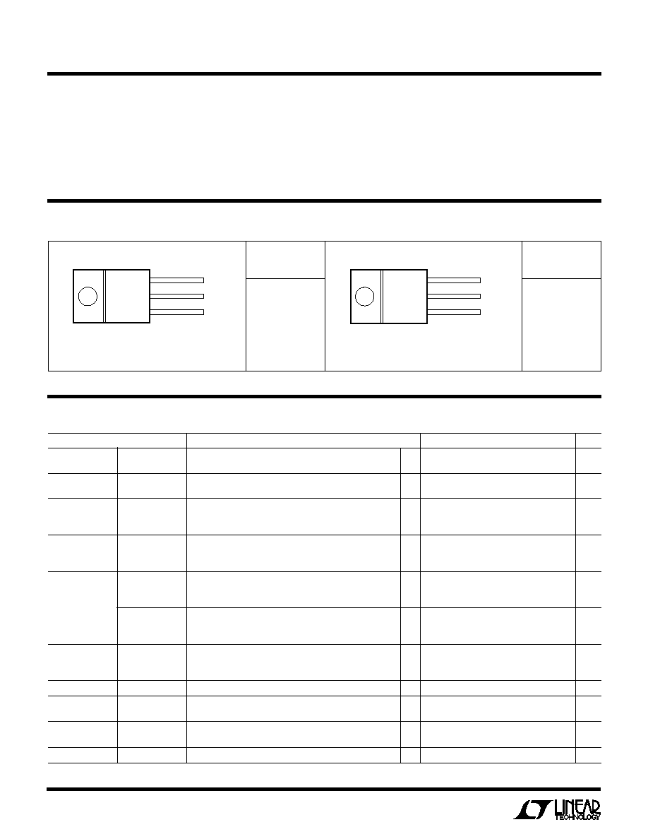
PACKAGE/ORDER I
N
FOR
M
ATIO
N
W
U
U
Consult factory for Industrial and Military grade parts.
ORDER PART
NUMBER
LT1585ACT
ORDER PART
NUMBER
LT1585ACT-3.3
JA
= 50
░
C/W
T PACKAGE
3-LEAD PLASTIC TO-220
FRONT VIEW
3
2
1
V
IN
V
OUT
GND
JA
= 50
░
C/W
T PACKAGE
3-LEAD PLASTIC TO-220
FRONT VIEW
3
2
1
V
IN
V
OUT
ADJ
PARAMETER
CONDITIONS
MIN
TYP
MAX
UNITS
Reference Voltage LT1585A
(V
IN
ş V
OUT
) = 3V, T
J
= 25
░
C, I
OUT
= 10mA
1.238 (ş1%)
1.250
1.262 (+1%)
V
1.5V
(V
IN
ş V
OUT
)
5.75V, 10mA
I
OUT
5A
q
1.225 (ş2%)
1.250
1.275 (+2%)
V
Output Voltage
LT1585A-3.3
V
IN
= 5V, T
J
= 25
░
C, I
OUT
= 0mA
3.267 (ş1%)
3.300
3.333 (+1%)
V
4.75V
V
IN
7V, 0mA
I
OUT
5A
q
3.235 (ş 2%)
3.300
3.365 (+ 2%)
V
Line Regulation
LT1585A
2.75V
V
IN
7V, I
OUT
= 10mA
(Notes 1, 2)
LT1585A-3.3
4.75V
V
IN
7V, I
OUT
= 0mA
q
0.005
0.2
%
Load Regulation
LT1585A
(V
N
ş V
OUT
) = 3V, T
J
= 25
░
C, 10mA
I
OUT
I
FULL LOAD
(Notes 1, 2, 3)
LT1585A-3.3
V
IN
= 5V, T
J
= 25
░
C, 0mA
I
OUT
I
FULL LOAD
0.05
0.3
%
q
0.05
0.5
%
Dropout Voltage
LT1585A
V
REF
= 1%, I
OUT
= 3A
LT1585A-3.3
V
OUT
= 1%, I
OUT
= 3A
q
1.150
1.300
V
LT1585A
V
REF
= 1%, I
OUT
= 5A
LT1585A-3.3
V
OUT
= 1%, I
OUT
= 5A
q
1.200
1.400
V
Current Limit
LT1585A
(V
IN
ş V
OUT
)
= 5.5V
(Note 3)
LT1585A-3.3
(V
IN
ş V
OUT
)
= 5.5V
q
5.0
6.0
A
Adjust Pin Current LT1585A
q
55
120
Á
A
Adjust Pin Current LT1585A
1.5V
(V
IN
ş V
OUT
)
5.75V, 10mA
I
OUT
I
FULL LOAD
q
0.2
5
Á
A
Change (Note 3)
Minimum
LT1585A
1.5V
(V
IN
ş V
OUT
)
5.75V
q
2
10
mA
Load Current
Quiescent Current
LT1585A-3.3
V
IN
= 5V
q
8
13
mA
ELECTRICAL CHARACTERISTICS

3
LT1585A/LT1585A-3.3
PARAMETER
CONDITIONS
MIN
TYP
MAX
UNITS
Ripple Rejection
LT1585A
f = 120Hz, C
OUT
= 25
Á
F Tant., (V
IN
ş V
OUT
) = 3V,
I
OUT
= 5A
LT1585A-3.3
f = 120Hz, C
OUT
= 25
Á
F Tant., V
IN
= 6.3V,
I
OUT
= 5A
q
60
72
dB
Thermal
LT1585A
T
A
= 25
░
C, 30ms Pulse
Regulation
LT1585A-3.3
T
A
= 25
░
C, 30ms Pulse
0.004
0.02
%/W
Temperature Stability
q
0.5
%
Long-Term Stability
T
A
= 125
░
C, 1000 Hrs.
0.03
1.0
%
RMS Output Noise
T
A
= 25
░
C, 10Hz
f
10kHz
0.003
%
(% of V
OUT
)
Thermal Resistance
LT1585A
T Package: Control Circuitry/Power Transistor
0.7/3.0
░
C/W
Junction to Case
ELECTRICAL CHARACTERISTICS
The
q
denotes specifications which apply over the specified operating
temperature range.
Note 1: See thermal regulation specifications for changes in output voltage
due to heating effects. Load and line regulation are measured at a constant
junction temperature by low duty cycle pulse testing.
Note 2: Line and load regulation are guaranteed up to the maximum power
dissipation 28.8W for the LT1585A in T package. Power dissipation is
determined by input/output differential and the output current. Guaranteed
maximum output power will not be available over the full input/output
voltage range.
Note 3: I
FULL LOAD
is defined as the maximum value of output load current
as a function of input-to-output voltage. I
FULL LOAD
is equal to 5A for the
LT1585A/LT1585A-3.3. The LT1585A has constant current limit with
changes in input-to-output voltage.
TYPICAL PERFOR
M
A
N
CE CHARACTERISTICS
U
W
TEMPERATURE (
░
C)
ş0.20
OUTPUT VOLTAGE DEVIATION (%)
ş0.10
0
0.10
ş0.15
ş0.05
0.05
ş25
25
75
125
LT1585A Ě TPC03
175
ş50
ş75
0
50
100
150
I = 5A
LT1585A Load Regulation
vs Temperature
OUTPUT CURRENT (A)
0
DROPOUT VOLTAGE (V)
1.1
1.3
1.5
4
LT1585A Ě TPC01
0.9
0.7
1.0
1.2
1.4
0.8
0.6
0.5
1
2
3
5
T = ş5
░
C
T = 125
░
C
T = 25
░
C
GUARANTEED
TEST POINTS
LT1585A Dropout Voltage
vs Output Current
TEMPERATURE (
░
C)
ş75
SHORT-CIRCUIT CURRENT (A)
5.0
5.5
125
LT1585A Ě TPC02
4.5
4.0
ş25
25 50
175
6.0
75
ş50
0
150
100
LT1585A Short-Circuit Current
vs Temperature

4
LT1585A/LT1585A-3.3
TYPICAL PERFOR
M
A
N
CE CHARACTERISTICS
U
W
LT1585A-3.3 Quiescent Current
vs Temperature
TEMPERATURE (
░
C)
ş75
QUIESCENT CURRENT (mA)
9
11
13
125
LT1585A Ě TPC09
7
5
8
10
12
6
4
3
ş25
25
75
ş50
150
0
50
100
175
LT1585A-3.3 Ripple Rejection
vs Frequency
FREQUENCY (Hz)
20
RIPPLE REJECTION (dB)
40
50
70
90
10
1k
10k
100k
LT1585A Ě TPC10
0
100
60
30
10
80
LT1585A-3.3: (V
IN
ş V
OUT
)
3V
0.5V
V
RIPPLE
2V
I
OUT
= I
FULL LOAD
LT1585A Maximum Power
Dissipation*
CASE TEMPERATURE (░C)
50
POWER (W)
20
25
30
80
100
LT1585A Ě TPC11
15
10
60 70
90
110 120 130 140 150
5
0
TEMPERATURE (
░
C)
ş75
REFERENCE VOLTAGE (V)
1.255
1.265
1.275
125
LT1585A Ě TPC04
1.245
1.235
1.250
1.260
1.270
1.240
1.230
1.225
ş25
25
75
ş50
150
0
50
100
175
LT1585A Reference Voltage
vs Temperature
LT1585A-3.3 Output Voltage
vs Temperature
TEMPERATURE (
░
C)
ş75
OUTPUT VOLTAGE (V)
3.33
3.34
3.35
125
LT1585A Ě TPC06
3.32
3.31
3.30
3.29
3.28
3.27
3.26
3.25
ş25
25
75
ş50
150
0
50
100
175
V
OUT
= 3.3V
Output Voltage vs Temperature
Using Adjustable LT1585A
TEMPERATURE (
░
C)
ş75
OUTPUT VOLTAGE (V)
3.60
3.65
3.70
125
LT1585A Ě TPC05
3.55
3.50
3.45
3.40
3.35
3.30
3.25
3.20
ş25
25
75
ş50
150
0
50
100
175
V
OUT
= 3.6V
V
OUT
= 3.45V
V
OUT
= 3.38V
V
OUT
= 3.3V
V
OUT
SET WITH 1% RESISTORS
LT1585A Adjust Pin Current
vs Temperature
TEMPERATURE (
░
C)
ş75
ADJUST PIN CURRENT (
Á
A)
60
80
100
125
LT1585A Ě TPC08
40
20
50
70
90
30
10
0
ş25
25
75
ş50
150
0
50
100
175
LT1585A Minimum Load Current
vs Temperature
TEMPERATURE (
░
C)
ş75
MINIMUM LOAD CURRENT (mA)
3
4
5
125
LT1585A Ě TPC07
2
1
0
ş25
25
75
ş50
150
0
50
100
175
*AS LIMITED BY MAXIMUM JUNCTION TEMPERATURE
5
LT1585A/LT1585A-3.3
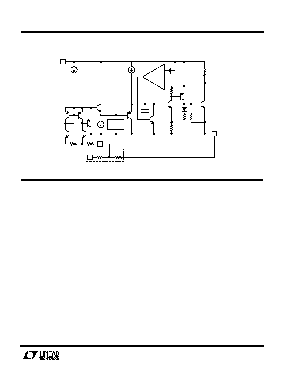
SI PLIFIED SCHE ATIC
W
W
THERMAL
LIMIT
GND
FOR FIXED VOLTAGE DEVICE
V
IN
V
OUT
LT1585A Ě BD
ADJ
ş
+
APPLICATIO
N
S I
N
FOR
M
ATIO
N
W
U
U
U
General
The LT1585A/LT1585A-3.3 3-terminal regulators are
easy to use and have all the protection features expected
in high performance linear regulators. The devices are
short-circuit protected, safe-area protected and provide
thermal shutdown to turn off the regulators should the
junction temperature exceed about 150
░
C. The regulators
include an adjustable and a fixed 3.3V version.
These ICs are pin compatible with the LT1083/LT1084/
LT1085 family of linear regulators but offer lower dropout
voltage and faster transient response. The trade-off for this
improved performance is a 7V maximum supply voltage.
Similar to the LT1083/LT1084/LT1085 family, the
LT1585A/LT1585A-3.3 regulators require an output ca-
pacitor for stability. However, the improved frequency
compensation permits the use of capacitors with much
lower ESR while still maintaining stability. This is critical in
addressing the needs of modern, low voltage, high speed
microprocessors.
Current generation microprocessors cycle load current
from almost zero to amps in tens of nanoseconds. Output
voltage tolerances are tighter and include transient re-
sponse as part of the specification. The LT1585A/
LT1585A-3.3 are specifically designed to meet the fast
current load-step requirements of these microprocessors
and save total cost by needing less output capacitance in
order to maintain regulation.
Stability
The circuit design in the LT1585A/LT1585A-3.3 requires
the use of an output capacitor as part of the frequency
compensation. For all operating conditions, the addition
of a 22
Á
F solid tantalum or a 100
Á
F aluminum electrolytic
on the output ensures stability. Normally, the LT1585A/
LT1585A-3.3 can use smaller value capacitors. Many
different types of capacitors are available and have widely
varying characteristics. These capacitors differ in capaci-
6
LT1585A/LT1585A-3.3
APPLICATIO
N
S I
N
FOR
M
ATIO
N
W
U
U
U
tor tolerance (sometimes ranging up to
▒
100%), equiva-
lent series resistance, equivalent series inductance and
capacitance temperature coefficient. The LT1585A/
LT1585A-3.3 frequency compensation optimizes fre-
quency response with low ESR capacitors. In general, use
capacitors with an ESR of less than 1
.
On the adjustable LT1585A, bypassing the adjust terminal
improves ripple rejection and transient response. Bypass-
ing the adjust pin increases the required output capacitor
value. The value of 22
Á
F tantalum or 100
Á
F aluminum
covers all cases of bypassing the adjust terminal. With no
adjust pin bypassing, smaller values of capacitors provide
equally good results.
Normally, capacitor values on the order of several hun-
dred microfarads are used on the output of the regulators
to ensure good transient response with heavy load current
changes. Output capacitance can increase without limit
and larger values of output capacitance further improve
the stability and transient response of the LT1585A/
LT1585A-3.3.
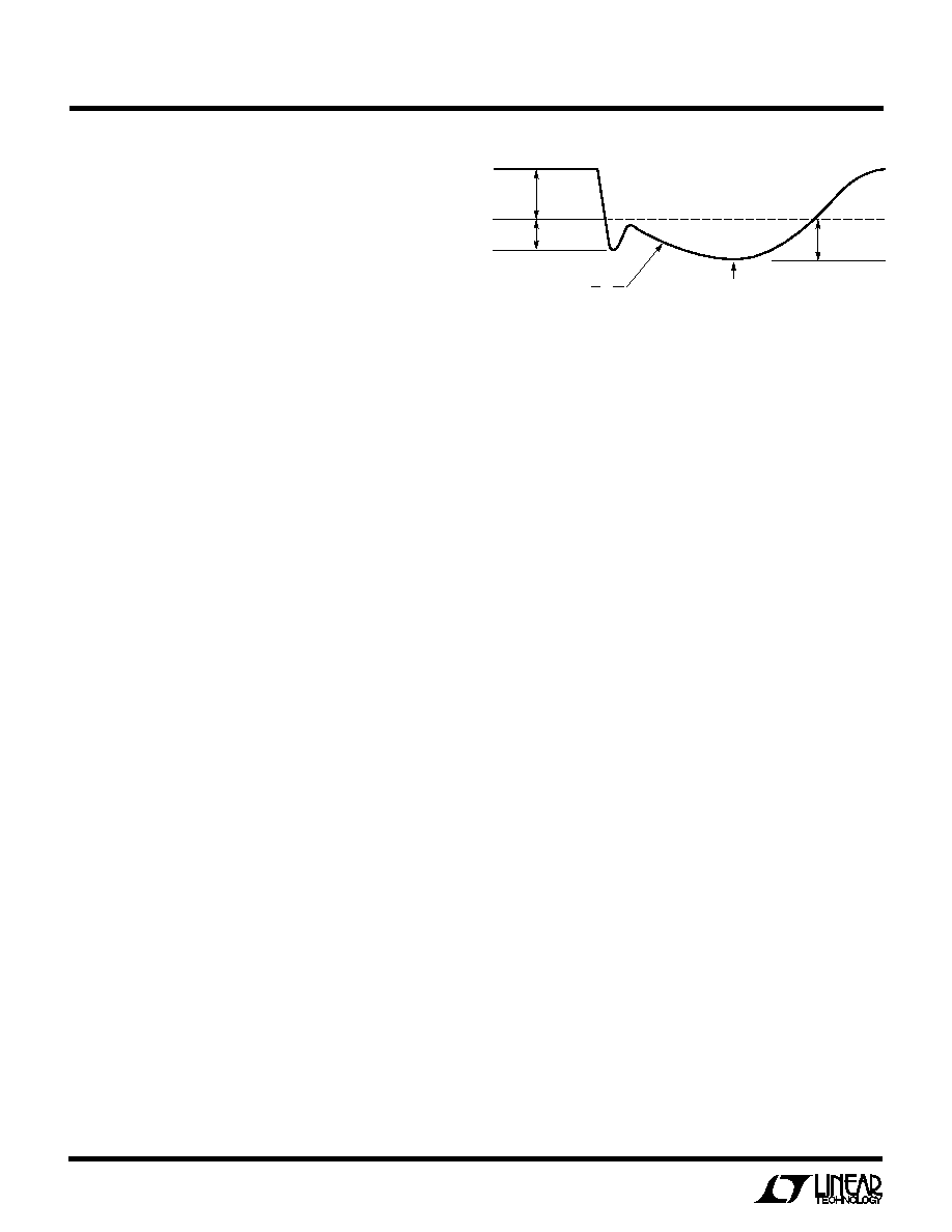
Large load current changes are exactly the situation
presented by modern microprocessors. The load current
step contains higher order frequency components that
the output decoupling network must handle until the
regulator throttles to the load current level. Capacitors are
not ideal elements and contain parasitic resistance and
inductance. These parasitic elements dominate the change
in output voltage at the beginning of a transient load step
change. The ESR of the output capacitors produces an
instantaneous step in output voltage (
V =
I Ě ESR). The
ESL of the output capacitors produces a droop propor-
tional to the rate of change of output current (V = L Ě
I/
t). The output capacitance produces a change in
output voltage proportional to the time until the regulator
can respond (
V =
t Ě
I/C). These transient effects are
illustrated in Figure 1.
The use of capacitors with low ESR, low ESL and good
high frequency characteristics is critical in meeting the
output voltage tolerances of these high speed micropro-
ESR
EFFECTS
LT1585A Ě F01
ESL
EFFECTS
CAPACITANCE
EFFECTS
POINT AT WHICH REGULATOR
TAKES CONTROL
SLOPE,
=
V
t
I
C
Figure 1
cessors. These requirements dictate a combination of
high quality, surface mount tantalum capacitors and
ceramic capacitors. The location of the decoupling net-
work is critical to transient response performance. Place
the decoupling network as close as possible to the pro-
cessor pins because trace runs from the decoupling
capacitors to the processor pins are inductive. The ideal
location for the decoupling network is actually inside the
microprocessor socket cavity. In addition, use large power
and ground plane areas to minimize distribution drops.
A possible stability problem that occurs in monolithic
linear regulators is current limit oscillations. The LT1585A/
LT1585A-3.3 essentially have a flat current limit over the
range of input supply voltage. The lower current limit
rating and 7V maximum supply voltage rating for these
devices permit this characteristic. Current limit oscilla-
tions are typically nonexistent, unless the input and out-
put decoupling capacitors for the regulators are mounted
several inches from the terminals.
Protection Diodes
In normal operation, the LT1585A/LT1585A-3.3 do not
require any protection diodes. Older 3-terminal regulators
require protection diodes between the output pin and the
input pin or between the adjust pin and the output pin to
prevent die overstress.
On the adjustable LT1585A, internal resistors limit inter-
nal current paths on the adjust pin. Therefore, even with
bypass capacitors on the adjust pin, no protection diode
is needed to ensure device safety under short-circuit
conditions.

7
LT1585A/LT1585A-3.3
APPLICATIO
N
S I
N
FOR
M
ATIO
N
W
U
U
U
A protection diode between the input and output pins is
usually not needed. An internal diode between the input
and output pins on the LT1585A/LT1585A-3.3 can handle
microsecond surge currents of 50A to 100A. Even with
large value output capacitors it is difficult to obtain those
values of surge currents in normal operation. Only with
large values of output capacitance, such as 1000
Á
F to
5000
Á
F, and with the input pin instantaneously shorted to
ground can damage occur. A crowbar circuit at the input
of the LT1585A/LT1585A-3.3 can generate those levels of
current, and a diode from output to input is then recom-
mended. This is shown in Figure 2. Usually, normal power
supply cycling or system "hot plugging and unplugging"
will not generate current large enough to do any damage.
The adjust pin can be driven on a transient basis
▒
7V with
respect to the output, without any device degradation. As
with any IC regulator, exceeding the maximum input-to-
output voltage differential causes the internal transistors
to break down and none of the protection circuitry is then
functional.
Ripple Rejection
The typical curve for ripple rejection reflects values for the
LT1585A-3.3 fixed output voltage part. In applications
that require improved ripple rejection, use the adjustable
device. A bypass capacitor from the adjust pin to ground
reduces the output ripple by the ratio of V
OUT
/1.25V. The
impedance of the adjust pin capacitor at the ripple fre-
quency should be less than the value of R1 (typically in the
range of 100
to 120
) in the feedback divider network
in Figure 2. Therefore, the value of the required adjust pin
capacitor is a function of the input ripple frequency. For
example, if R1 equals 100
and the ripple frequency
equals 120Hz, the adjust pin capacitor should be 22
Á
F. At
10kHz, only 0.22
Á
F is needed.
Output Voltage
The LT1585A adjustable regulator develops a 1.25V ref-
erence voltage between the output pin and the adjust pin
(see Figure 3). Placing a resistor R1 between these two
terminals causes a constant current to flow through R1
and down through R2 to set the overall output voltage.
Normally, this current is the specified minimum load
current of 10mA. The current out of the adjust pin adds to
the current from R1 and is typically 55
Á
A. Its output
voltage contribution is small and only needs consider-
ation when very precise output voltage setting is required.
LT1585A-3.3
D1
1N4002
(OPTIONAL)
GND
V
IN
V
OUT
IN
OUT
C1
10
Á
F
+
C2
10
Á
F
+
LT1585A
D1
1N4002
(OPTIONAL)
ADJ
V
IN
V
OUT
IN
OUT
LT1585A Ě F02
C1
10
Á
F
+
C2
10
Á
F
R1
R2
+
C
ADJ
+
Figure 2
LT1585A
ADJ
V
IN
V
OUT
IN
R1
V
REF
R2
V
OUT
= V
REF
(1 + R2/R1) + I
ADJ
(R2)
OUT
I
ADJ
55
Á
A
LT1585A Ě F03
C1
10
Á
F
+
C2
10
Á
F
+
Figure 3. Basic Adjustable Regulator
8
LT1585A/LT1585A-3.3
APPLICATIO
N
S I
N
FOR
M
ATIO
N
W
U
U
U
load regulation is obtained when the top of resistor divider
R1 connects directly to the regulator output and not to the
load. Figure 5 illustrates this point. If R1 connects to the
load, the effective resistance between the regulator and
the load is:
R
P
(1 + R2/R1), R
P
= Parasitic Line Resistance
The connection shown in Figure 5 does not multiply R
P
by
the divider ratio. As an example, R
P
is about four milliohms
per foot with 16-gauge wire. This translates to 4mV per
foot at 1A load current. At higher load currents, this drop
represents a significant percentage of the overall regula-
tion. It is important to keep the positive lead between the
regulator and the load as short as possible and to use large
wire or PC board traces.
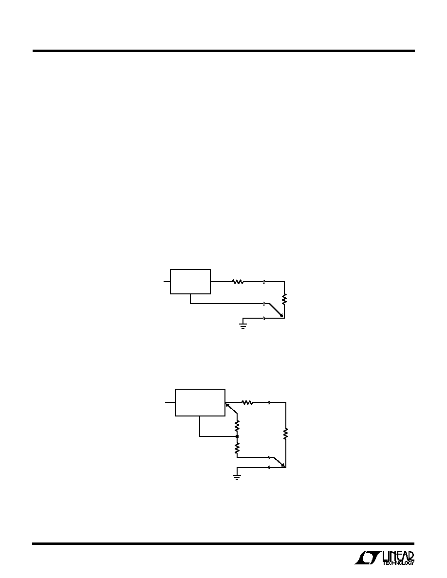
Load Regulation
It is not possible to provide true remote load sensing
because the LT1585A/LT1585A-3.3 are 3-terminal de-
vices. Load regulation is limited by the resistance of the
wire connecting the regulators to the load. Load regula-
tion per the data sheet specification is measured at the
bottom of the package.
For fixed voltage devices, negative side sensing is a true
Kelvin connection with the ground pin of the device
returned to the negative side of the load. This is illustrated
in Figure 4.
For adjustable voltage devices, negative side sensing is a
true Kelvin connection with the bottom of the output
divider returned to the negative side of the load. The best
LT1585A-3.3
R
P
PARASITIC
LINE RESISTANCE
GND
V
IN
R
L
IN
OUT
LT1585A Ě F04
Figure 4. Connection for Best Load Regulation
LT1585A
OUT
IN
V
IN
ADJ
R
P
PARASITIC
LINE RESISTANCE
R1*
*CONNECT R1 TO CASE
CONNECT R2 TO LOAD
LT1585A Ě F05
R
L
R2*
Figure 5. Connection for Best Load Regulation

9
LT1585A/LT1585A-3.3
Thermal Considerations
The LT1585A/LT1585A-3.3 family protects the device
under overload conditions with internal power and ther-
mal limiting circuitry. However, for normal continuous
load conditions, do not exceed maximum junction tem-
perature ratings. It is important to consider all sources of
thermal resistance from junction-to-ambient. These
sources include the junction-to-case resistance, the case-
to-heat sink interface resistance and the heat sink resis-
tance. Thermal resistance specifications have been devel-
oped to more accurately reflect device temperature and
ensure safe operating temperatures. The Electrical Char-
acteristics section provides a separate thermal resistance
and maximum junction temperature for both the control
circuitry and the power transistor. Older regulators, with
a single junction-to-case thermal resistance specifica-
tion, use an average of the two values provided here and
allow excessive junction temperatures under certain con-
ditions of ambient temperature and heat sink resistance.
Calculate the maximum junction temperature for both
sections to ensure that both thermal limits are met.
Junction-to-case thermal resistance is specified from the
IC junction to the bottom of the case directly below the die.
This is the lowest resistance path for heat flow. Proper
mounting ensures the best thermal flow from this area of
the package to the heat sink. Linear Technology strongly
recommends thermal compound at the case-to-heat sink
interface. Use a thermally conductive spacer if the case of
the device must be electrically isolated and include its
contribution to the total thermal resistance. Please con-
sult "Mounting Considerations for Power Semiconduc-
tors"
1990 Linear Applications Handbook, Volume I,
Pages RR3-1 to RR3-20. The output connects to the case
of both the LT1585A and the LT1585A-3.3.
For example, using an LT1585ACT-3.3 (TO-220, com-
mercial) and assuming:
V
IN
(Max Continuous) = 5.25V (5V + 5%), V
OUT
= 3.3V,
I
OUT
= 5A
T
A
= 70
░
C,
HEAT SINK
= 3
░
C/W
CASE-TO-HEAT SINK
= 1
░
C/W (with Thermal Compound)
Power dissipation under these conditions is equal to:
P
D
= (V
IN
ş V
OUT
)(I
OUT
) = (5.25 ş 3.3)(5) = 9.75W
Junction temperature will be equal to:
T
J
=
T
A
+ P
D
(
HEAT SINK
+
CASE-TO-HEAT SINK
+
JC
)
For the Control Section:
T
J
= 70
░
C + 9.75W (3
░
C/W + 1
░
C/W + 0.7
░
C/W)
= 115.8
░
C
115.8
░
C < 125
░
C = T
JMAX
(Control Section Commer-
cial range)
For the Power Transistor:
T
J
=
70
░
C
+ 9.75W (3
░
C/W + 1
░
C/W + 3
░
C/W)
= 138.3
░
C
138.3
░
C < 150
░
C = T
JMAX
(Power Transistor Com-
mercial Range)
In both cases the junction temperature is below the
maximum rating for the respective sections, ensuring
reliable operation.
APPLICATIO
N
S I
N
FOR
M
ATIO
N
W
U
U
U
10
LT1585A/LT1585A-3.3
TYPICAL APPLICATIO
N
S
N
U
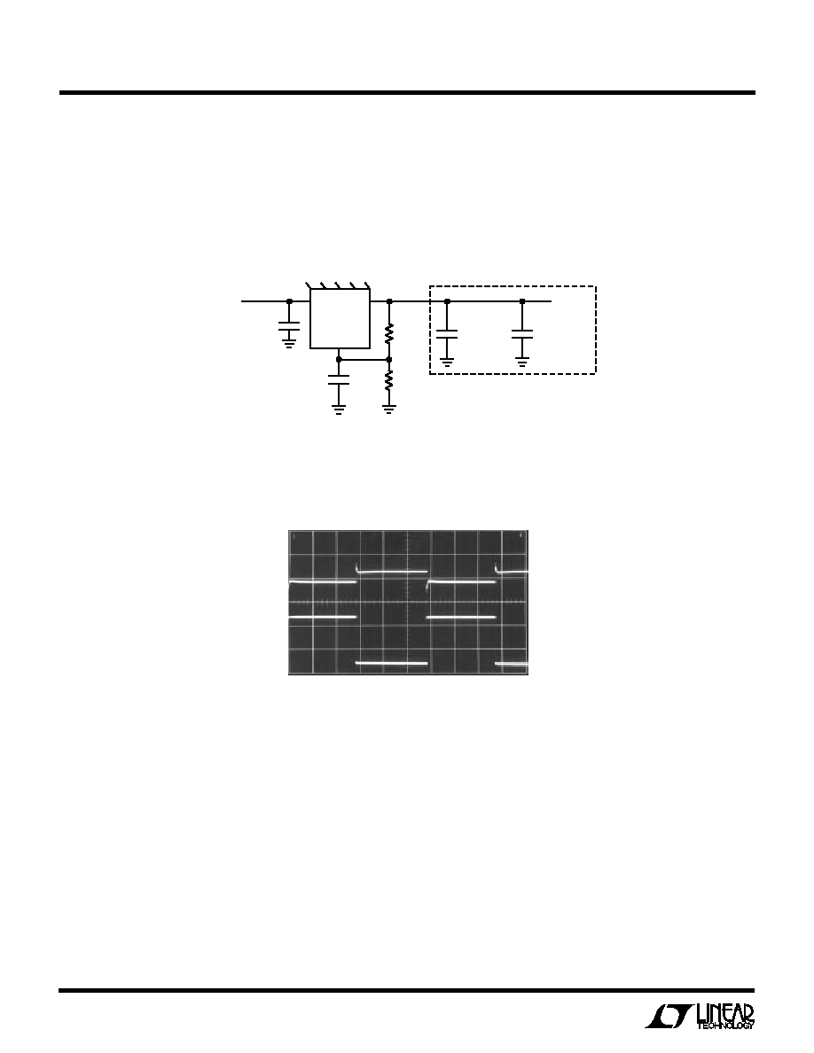
Minimum Parts Count LT1585A Adjustable Circuit
for the Intel 120MHz Pentium Processor
LT1585ACT
ADJ
IN
AVX CORP. (803) 448-9411
THERMALLOY INC. (214) 243-4321
DO NOT SUBSTITUTE COMPONENTS.
C1 TO C3
220
Á
F
10V
AVX TPS
3 EACH
R1
110
0.1%
C4
330nF
16V
AVX X7R 0805
OUT
4.75V TO
5.25V
THERMALLOY
7020B-MT
PLACE IN MICROPROCESSOR
SOCKET CAVITY
+
C5 TO C10
100
Á
F
10V
AVX TPS
4 EACH
+
C11 TO C20
1
Á
F
16V
AVX Y5V 0805
24 EACH
R2
197
0.1%
3.50V
5A
LT1585A TA04
LT1585A Transient Response
for 3.8A Load Current Step*
V
OUT
50mV/DIV
I
OUT
2A/DIV
100
Á
s/DIV
*TRANSIENT RESPONSE MEASURED WITH AN INTEL
POWER VALIDATOR. V
OUT
IS MEASURED AT THE
POWER VALIDATOR
LT1584A Ě TA05
11
LT1585A/LT1585A-3.3
Information furnished by Linear Technology Corporation is believed to be accurate and reliable.
However, no responsibility is assumed for its use. Linear Technology Corporation makes no represen-
tation that the interconnection of its circuits as described herein will not infringe on existing patent rights.
TYPICAL APPLICATIO
N
S
N
U
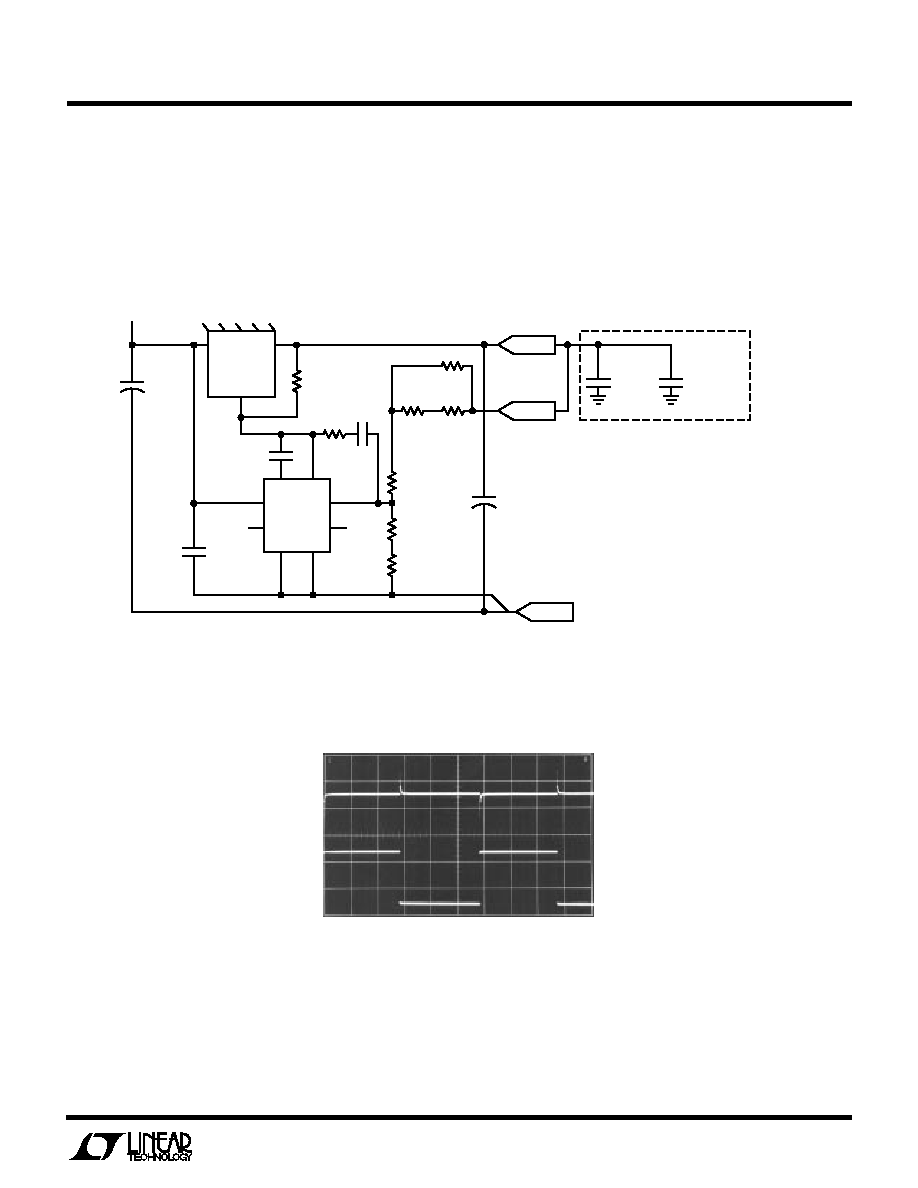
Guaranteed LT1585A Circuit for the Intel 100MHz and Higher Frequency Pentium Processors
(Meets Intel Specifications with Worst-Case Tolerances)
+
+
LT1585A
ADJ
IN
R1
1k
C2 TO C4
220
Á
F
10V
AVX TPS
3 EACH
5V
OUT
3
SEE NOTE 6
SEE NOTE 5
SEE NOTE 7
2
1
2
R2
1k
R4
6
5
4
3
2
1
R3E
117
R3D
83
C6
0.01
Á
F
C1
0.1
Á
F
C5
33pF
NPO
1
5
6
8
7
3
4
R3C
800
R3B
1.35k
R3A
1.15k
LT1431S
COMP COL
SGND FGND
V
+
REF
R
T
R
M
PGND
SGND
LT1584 Ě TA06
PGND
SENSE
V
OUT
PLACE IN MICROPROCESSOR
SOCKET CAVITY
C14 TO C23
1
Á
F
16V
AVX Y5V 0805
24 EACH
+
C8 TO C13
100
Á
F
10V
AVX TPS
4 EACH
NOTES: UNLESS OTHERWISE SPECIFIED
1. ALL RESISTOR VALUES ARE OHMS,
1/8W, 5%
2. ALL CAPACITORS ARE 50V, 20%
3. ALL POLARIZED CAPACITORS ARE AVX
TYPE TPS OR EQUIVALENT
4. INPUT CAPACITANCE MAY BE REDUCED
IF THE 5V SUPPLY IS WELL BYPASSED
5. FOR 100MHz PENTIUM PROCESSOR,
INPUT VOLTAGE MUST BE AT LEAST
4.85V AT THE REGULATOR INPUT
6. FOR PENTIUM VRE PROCESSOR,
R4 NOT INSTALLED
ş FOR 3.3V OUTPUT, INSTALL 0
JUMPER
RESISTOR R4
7. R3A TO R3E ARE B.I. TECHNOLOGY 627V100
+
C7
100
Á
F
10V
THERMALLOY
7021B-MT
LT1585A/LT1431 Transient Response
for 3.8A Load Current Step*
V
OUT
50mV/DIV
I
OUT
2A/DIV
100
Á
s/DIV
LT1584A Ě TA06
*TRANSIENT RESPONSE MEASURED WITH AN INTEL
POWER VALIDATOR. V
OUT
IS MEASURED AT THE
POWER VALIDATOR

12
LT1585A/LT1585A-3.3
LT/GP 1095 10K Ě PRINTED IN USA
ę
LINEAR TECHNOLOGY CORPORATION 1995
Linear Technology Corporation
1630 McCarthy Blvd., Milpitas, CA 95035-7487
(408) 432-1900
q
FAX
: (408) 434-0507
q
TELEX
: 499-3977
PACKAGE DESCRIPTIO
N
U
Dimensions in inches (millimeters) unless otherwise noted.
RELATED PARTS
PART NUMBER
DESCRIPTION
COMMENTS
LTC1430
High Power Step-Down Switching Regulator
5V to 3.3V at 10A
LT1580
7A Very Low Dropout Linear Regulator
0.54V Dropout at 7A, Fixed 2.5V
OUT
and Adjustable
LT1584
7A Low Dropout Fixed and Adjustable Linear Regulators
Fast Transient Response for Microprocessor Applications
LT1587
3A Low Dropout Fixed and Adjustable Linear Regulators
Fast Transient Response for Microprocessor Applications
T Package
3-Lead Plastic TO-220
0.090 ş 0.110
(2.286 ş 2.794)
0.028 ş 0.038
(0.711 ş 0.965)
T3 (TO-220) 0595
0.045 ş 0.055
(1.143 ş 1.397)
0.165 ş 0.180
(4.293 ş 4.699)
0.095 ş 0.115
(2.413 ş 2.921)
0.013 ş 0.023
(0.330 ş 0.584)
0.520 ş 0.570
(13.208 ş 14.478)
0.980 ş 1.070
(24.892 ş 27.178)
0.218 ş 0.252
(5.537 ş 6.401)
0.050
(1.270)
TYP
0.147 ş 0.155
(3.734 ş 3.937)
DIA
0.390 ş 0.415
(9.906 ş 10.541)
0.330 ş 0.370
(8.382 ş 9.398)
0.460 ş 0.500
(11.684 ş 12.700)
0.570 ş 0.620
(14.478 ş 15.748)
0.230 ş 0.270
(5.842 ş 6.858)