Äîêóìåíòàöèÿ è îïèñàíèÿ www.docs.chipfind.ru
LT1469
1
Information furnished by Linear Technology Corporation is believed to be accurate and reliable.
However, no responsibility is assumed for its use. Linear Technology Corporation makes no represen-
tation that the interconnection of its circuits as described herein will not infringe on existing patent rights.
The LT
®
1469 is a dual, precision high speed operational
amplifier with 16-bit accuracy and 900ns settling to 150
µ
V
for 10V signals. This unique blend of precision and AC
performance makes the LT1469 the optimum choice for
high accuracy applications such as DAC current-to-volt-
age conversion and ADC buffers. The initial accuracy and
drift characteristics of the input offset voltage and invert-
ing input bias current are tailored for inverting applica-
tions.
The 90MHz gain bandwidth ensures high open-loop gain
at frequency for reducing distortion. In noninverting appli-
cations such as an ADC buffer, the low distortion and DC
accuracy allow full 16-bit AC and DC performance.
The 22V/
µ
s slew rate of the LT1469 improves large signal
performance compared to other precision op amps in
applications such as active filters and instrumentation
amplifiers.
The LT1469 is manufactured on Linear Technology's
complementary bipolar process and is available in 8-pin
PDIP and SO packages. A single version,the LT1468, is
also available.
s
Precision Instrumentation
s
High Accuracy Data Acquisition Systems
s
16-Bit DAC Current-to-Voltage Converter
s
ADC Buffer
s
Low Distortion Active Filters
s
Photodiode Amplifiers
, LTC and LT are registered trademarks of Linear Technology Corporation.
s
90MHz Gain Bandwidth, f = 100kHz
s
Maximum Input Offset Voltage: 125
µ
V
s
Settling Time: 900ns (A
V
= 1, 150
µ
V, 10V Step)
s
22V/
µ
s Slew Rate
s
Low Distortion: 96.5dB for 100kHz, 10V
P-P
s
Maximum Input Offset Voltage Drift: 3
µ
V/
°
C
s
Maximum Inverting Input Bias Current: 10nA
s
Minimum DC Gain: 300V/mV
s
Minimum Output Swing into 2k:
±
12.8V
s
Unity-Gain Stable
s
Input Noise Voltage: 5nV/
Hz
s
Input Noise Current: 0.6pA/
Hz
s
Total Input Noise Optimized for 1k
< R
S
< 20k
s
Specified at
±
5V and
±
15V Supplies
APPLICATIO S
U
FEATURES
DESCRIPTIO
U
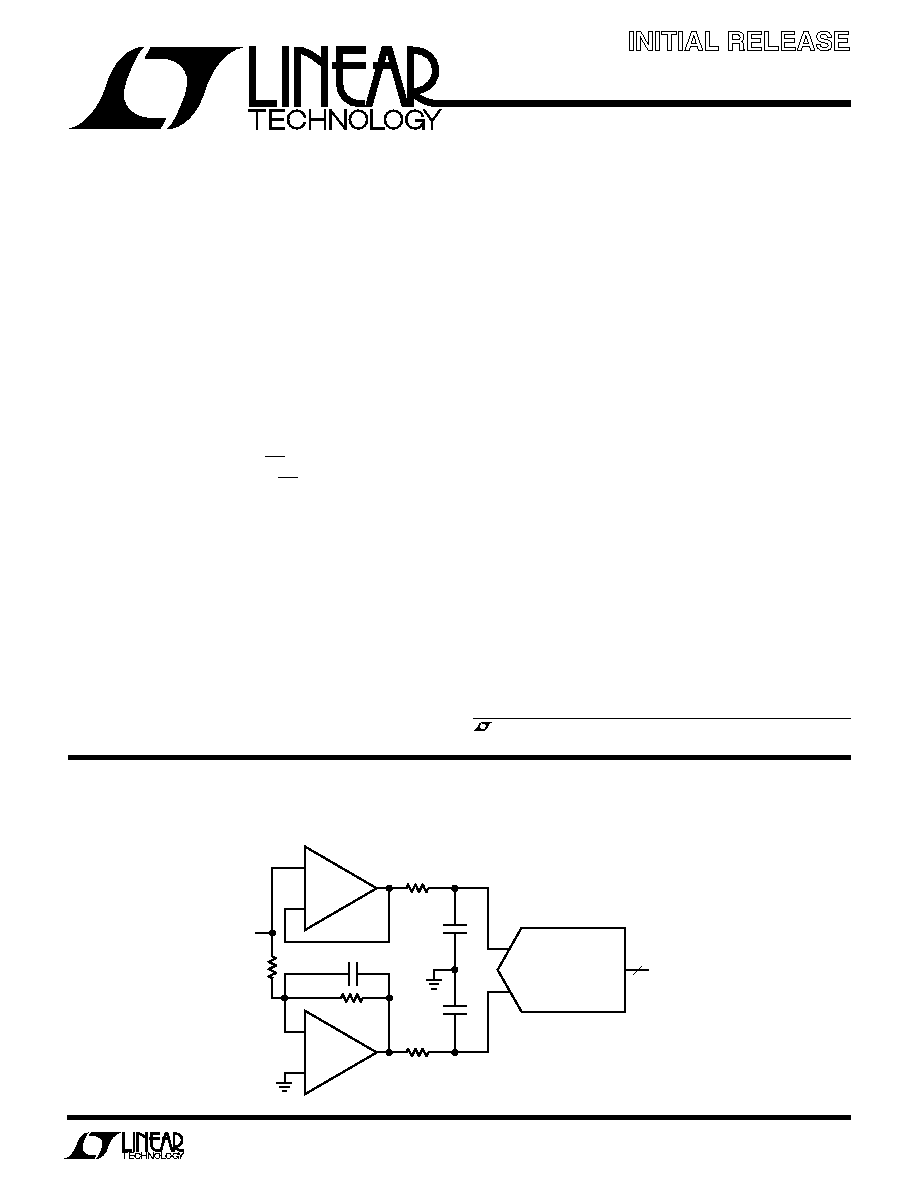
TYPICAL APPLICATIO
U
Dual 90MHz, 22V/
µ
s
16-Bit Accurate Operational Amplifier
February 2000
Final Electrical Specifications
+
+
2k
V
IN
2k
10pF
200
200
300pF
300pF
+IN
LTC1604
1/2 LT1469
1/2 LT1469
16 BITS
333ksps
1469 TA01
IN
16-Bit Accurate Single Ended to Differential ADC Buffer
LT1469
2
Total Supply Voltage (V
+
to V
) .............................. 36V
Input Current (Note 2) ........................................
±
10mA
Output Short-Circuit Duration (Note 3) ............ Indefinite
Operating Temperature Range (Note 4) .. 40
°
C to 85
°
C
Specified Temperature Range (Note 5) ... 40
°
C to 85
°
C
Maximum Junction Temperature .......................... 150
°
C
Storage Temperature Range ................. 65
°
C to 150
°
C
Lead Temperature (Soldering, 10 sec).................. 300
°
C
ORDER PART
NUMBER
S8 PART MARKING
T
JMAX
= 150
°
C,
JA
= 130
°
C/W (N8)
T
JMAX
= 150
°
C,
JA
= 190
°
C/W (S8)
Consult factory for Military grade parts.
1469
1469I
LT1469CS8
LT1469IS8
LT1469CN8
LT1469IN8
ABSOLUTE AXI U
RATI GS
W
W
W
U
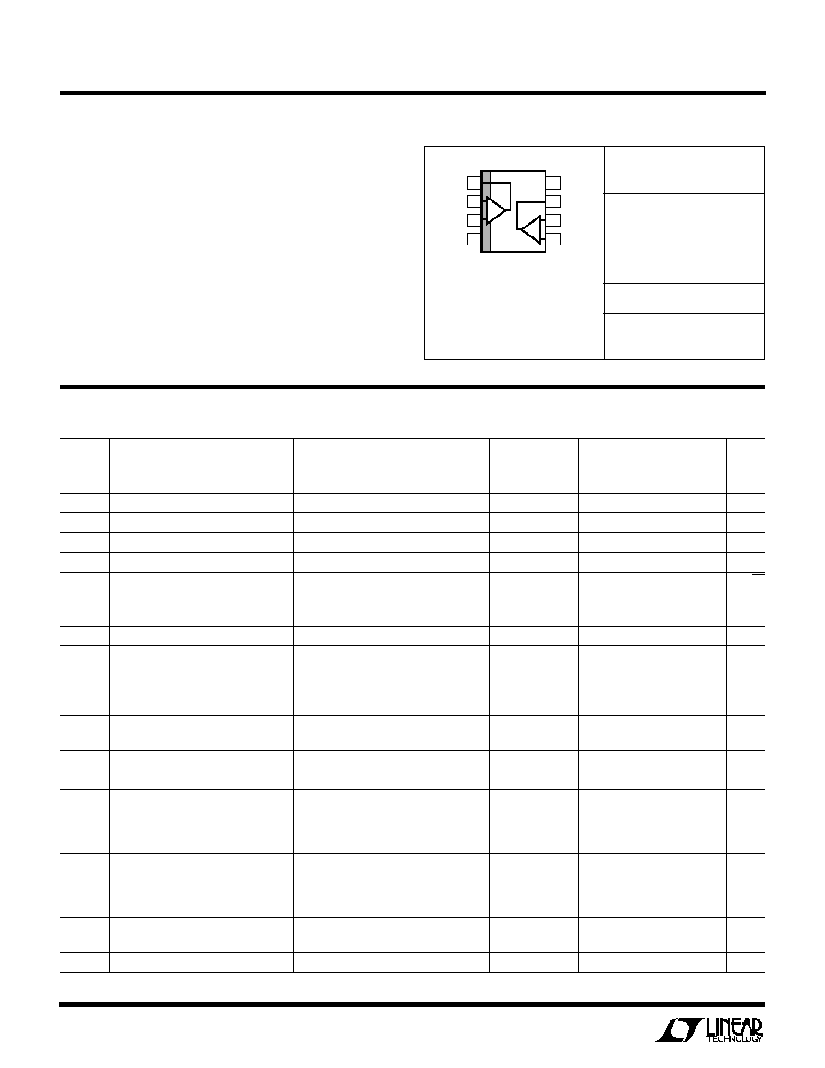
PACKAGE/ORDER I FOR ATIO
U
U
W
(Note 1)
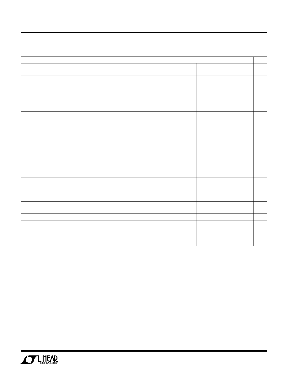
ELECTRICAL CHARACTERISTICS
T
A
= 25
°
C, V
CM
= 0V unless otherwise noted.
SYMBOL
PARAMETER
CONDITIONS
V
SUPPLY
MIN
TYP
MAX
UNITS
V
OS
Input Offset Voltage
±
15V
30
125
µ
V
±
5V
50
200
µ
V
I
OS
Input Offset Current
±
5V to
±
15V
13
±
50
nA
I
B
Inverting Input Bias Current
±
5V to
±
15V
3
±
10
nA
I
B
+
Noninverting Input Bias Current
±
5V to
±
15V
10
±
40
nA
e
n
Input Noise Voltage Density
f = 10kHz
±
5V to
±
15V
5
nV/
Hz
i
n
Input Noise Current Density
f = 10kHz
±
5V to
±
15V
0.6
pA/
Hz
R
IN
Input Resistance
V
CM
=
±
12.5V
±
15V
100
240
M
Differential
±
15V
50
150
k
C
IN
Input Capacitance
±
15V
4
pF
V
CM
Input Voltage Range (Positive)
±
15V
12.5
13.5
V
±
5V
2.5
3.5
V
Input Voltage Range (Negative)
±
15V
14.3
12.5
V
±
5V
4.3
2.5
V
CMRR
Common Mode Rejection Ratio
V
CM
=
±
12.5V
±
15V
96
110
dB
V
CM
=
±
2.5V
±
5V
96
112
dB
Minimum Supply Voltage
Guaranteed by PSRR
±
2.5
±
4.5
V
PSRR
Power Supply Rejection Ratio
V
S
=
±
4.5V to
±
15V
100
112
dB
A
VOL
Large-Signal Voltage Gain
V
OUT
=
±
12.5V, R
L
= 10k
±
15V
300
9000
V/mV
V
OUT
=
±
12.5V, R
L
= 2k
±
15V
300
5000
V/mV
V
OUT
=
±
2.5V, R
L
= 10k
±
5V
200
6000
V/mV
V
OUT
=
±
2.5V, R
L
= 2k
±
5V
200
3000
V/mV
V
OUT
Maximum Output Swing
R
L
= 10k, 1mV Overdrive
±
15V
±
13
±
13.6
V
R
L
= 2k, 1mV Overdrive
±
15V
±
12.8
±
13.5
V
R
L
= 10k, 1mV Overdrive
±
5V
±
3
±
3.6
V
R
L
= 2k, 1mV Overdrive
±
5V
±
2.8
±
3.5
V
I
OUT
Maximum Output Current
V
OUT
=
±
12.5V, 1mV Overdrive
±
15V
±
15
±
22
mA
V
OUT
=
±
2.5V, 1mV Overdrive
±
5V
±
15
±
22
mA
I
SC
Output Short-Circuit Current
V
OUT
= 0V, 0.2V Overdrive (Note 3)
±
15V
±
25
±
40
mA
1
2
3
4
8
7
6
5
TOP VIEW
V+
OUT B
IN B
+IN B
OUT A
IN A
+IN A
V
S8 PACKAGE
8-LEAD PLASTIC SO
A
B
LT1469
3
SYMBOL
PARAMETER
CONDITIONS
V
SUPPLY
MIN
TYP
MAX
UNITS
ELECTRICAL CHARACTERISTICS
T
A
= 25
°
C, V
CM
= 0V unless otherwise noted.
SYMBOL
PARAMETER
CONDITIONS
V
SUPPLY
MIN
TYP
MAX
UNITS
V
OS
Input Offset Voltage
±
15V
q
350
µ
V
±
5V
q
350
µ
V
V
OS
/
T
Input Offset Voltage Drift
(Note 8)
±
5V to
±
15V
q
1
3
µ
V/
°
C
I
OS
Input Offset Current
±
5V to
±
15V
q
±
80
nA
I
OS
/
T
Input Offset Current Drift
(Note 8)
±
5V to
±
15V
q
60
pA/
°
C
I
B
Inverting Input Bias Current
±
5V to
±
15V
q
±
20
nA
I
B
/
T
Inverting Input Bias Current Drift
(Note 8)
±
5V to
±
15V
q
40
pA/
°
C
I
B
+
Noninverting Input Bias Current
±
5V to
±
15V
q
±
60
nA
V
CM
Input Voltage Range (Positive)
±
15V
q
12.5
V
±
5V
q
2.5
V
Input Voltage Range (Negative)
±
15V
q
12.5
V
±
5V
q
2.5
V
CMRR
Common Mode Rejection Ratio
V
CM
=
±
12.5V
±
15V
q
94
dB
V
CM
=
±
2.5V
±
5V
q
94
dB
SR
Slew Rate
A
V
= 10, R
L
= 2k (Note 6)
±
15V
15
22
V/
µ
s
±
5V
11
17
V/
µ
s
FPBW
Full-Power Bandwidth
10V Peak, (Note 7)
±
15V
350
kHz
3V Peak, (Note 7)
±
5V
900
kHz
GBW
Gain Bandwidth Product
f = 100kHz, R
L
= 2k
±
15V
60
90
MHz
±
5V
55
88
MHz
t
r
, t
f
Rise Time, Fall Time
A
V
= 1, 10% to 90%, 0.1V
±
15V
11
ns
±
5V
12
ns
OS
Overshoot
A
V
= 1, 0.1V
±
15V
30
%
±
5V
35
%
t
PD
Propagation Delay
A
V
= 1, 50% V
IN
to 50% V
OUT
, 0.1V
±
15V
9
ns
±
5V
10
ns
t
S
Settling Time
10V Step, 0.01%, A
V
= 1
±
15V
760
ns
10V Step, 150
µ
V, A
V
= 1
±
15V
900
ns
5V Step, 0.01%, A
V
= 1
±
5V
770
ns
THD
Total Harmonic Distortion
A
V
= 1, 10V
P-P
, 100kHz
±
15V
96.5
dB
R
OUT
Output Resistance
A
V
= 1, f = 100kHz
±
15V
0.02
Channel Separation
V
OUT
=
±
12.5V, R
L
= 2k
±
15V
100
120
dB
V
OUT
=
±
2.5V, R
L
= 2k
±
5V
100
120
dB
I
S
Supply Current
Per Amplifier
±
15V
4.1
5.2
mA
±
5V
3.8
5
mA
V
OS
Input Offset Voltage Match
±
15V
225
µ
V
±
5V
350
µ
V
I
B
Inverting Input Bias Current Match
±
5V to
±
15V
±
18
nA
I
B
+
Noninverting Input Bias Current Match
±
5V to
±
15V
±
78
nA
CMRR
Common Mode Rejection Match
V
CM
=
±
12.5V (Note 9)
±
15V
93
dB
V
CM
=
±
2.5V (Note 9)
±
5V
93
dB
PSRR
Power Supply Rejection Match
V
S
=
±
4.5V to
±
15V (Note 9)
97
dB
The
q
denotes the specifications which apply over the temperature range 0
°
C
T
A
70
°
C, V
CM
= 0V unless otherwise noted.
LT1469
4
SYMBOL
PARAMETER
CONDITIONS
V
SUPPLY
MIN
TYP
MAX
UNITS
The
q
denotes the specifications which apply over the temperature range
0
°
C
T
A
70
°
C, V
CM
= 0V unless otherwise noted.
ELECTRICAL CHARACTERISTICS
Minimum Supply Voltage
Guaranteed by PSRR
q
±
4.5
V
PSRR
Power Supply Rejection Ratio
V
S
=
±
4.5V to
±
15V
q
95
dB
A
VOL
Large-Signal Voltage Gain
V
OUT
=
±
12.5V, R
L
= 10k
±
15V
q
100
V/mV
V
OUT
=
±
12.5V, R
L
= 2k
±
15V
q
100
V/mV
V
OUT
=
±
2.5V, R
L
= 10k
±
5V
q
100
V/mV
V
OUT
=
±
2.5V, R
L
= 2k
±
5V
q
100
V/mV
V
OUT
Maximum Output Swing
R
L
= 10k, 1mV Overdrive
±
15V
q
±
12.9
V
R
L
= 2k, 1mV Overdrive
±
15V
q
±
12.7
V
R
L
= 10k, 1mV Overdrive
±
5V
q
±
2.9
V
R
L
= 2k, 1mV Overdrive
±
5V
q
±
2.7
V
I
OUT
Maximum Output Current
V
OUT
=
±
12.5V, 1mV Overdrive
±
15V
q
±
12.5
mA
V
OUT
=
±
2.5V, 1mV Overdrive
±
5V
q
±
12.5
mA
I
SC
Output Short-Circuit Current
V
OUT
= 0V, 0.2V Overdrive (Note 3)
±
15V
q
±
17
mA
SR
Slew Rate
A
V
= 10, R
L
= 2k (Note 6)
±
15V
q
13
V/
µ
s
±
5V
q
9
V/
µ
s
GBW
Gain Bandwidth Product
f = 100kHz, R
L
= 2k
±
15V
q
55
MHz
±
5V
q
50
MHz
Channel Separation
V
OUT
=
±
12.5V, R
L
= 2k
±
15V
q
98
dB
V
OUT
=
±
2.5V, R
L
= 2k
±
5V
q
98
dB
I
S
Supply Current
Per Amplifier
±
15V
q
6.5
mA
±
5V
q
6.3
mA
V
OS
Input Offset Voltage Match
±
15V
q
600
µ
V
±
5V
q
600
µ
V
I
B
Inverting Input Bias Current Match
±
5V to
±
15V
q
±
38
nA
I
B
+
Noninverting Input Bias Current Match
±
5V to
±
15V
q
±
118
nA
CMRR
Common Mode Rejection Match
V
CM
=
±
12.5V (Note 9)
±
15V
q
91
dB
V
CM
=
±
2.5V (Note 9)
±
5V
q
91
dB
PSRR
Power Supply Rejection Match
V
S
=
±
4.5V to
±
15V (Note 9)
q
92
dB
SYMBOL
PARAMETER
CONDITIONS
V
SUPPLY
MIN
TYP
MAX
UNITS
V
OS
Input Offset Voltage
±
15V
q
500
µ
V
±
5V
q
500
µ
V
V
OS
/
T
Input Offset Voltage Drift
(Note 8)
±
5V to
±
15V
q
1
4
µ
V/
°
C
I
OS
Input Offset Current
±
5V to
±
15V
q
±
120
nA
I
OS
/
T
Input Offset Current Drift
(Note 8)
±
5V to
±
15V
q
120
pA/
°
C
I
B
Inverting Input Bias Current
±
5V to
±
15V
q
±
40
nA
I
B
/
T
Inverting Input Bias Current Drift
(Note 8)
±
5V to
±
15V
q
80
pA/
°
C
I
B
+
Noninverting Input Bias Current
±
5V to
±
15V
q
±
80
nA
V
CM
Input Voltage Range (Positive)
±
15V
q
12.5
V
±
5V
q
2.5
V
Input Voltage Range (Negative)
±
15V
q
12.5
V
±
5V
q
2.5
V
The
q
denotes the specifications which apply over the temperature range 40
°
C
T
A
85
°
C, V
CM
= 0V unless otherwise noted.
(Note 5)
LT1469
5
The
q
denotes the specifications which apply over the temperature range
40
°
C
T
A
85
°
C, V
CM
= 0V unless otherwise noted. (Note 5)
Note 1: Absolute Maximum Ratings are those values beyond which the life
of a device may be impaired.
Note 2: The inputs are protected by back-to-back diodes and two 100
series resistors. If the differential input voltage exceeds 0.7V, the input
current should be limited to less than 10mA. Input voltages outside the
supplies will be clamped by ESD protection devices and input currents
should also be limited to less than 10mA.
Note 3: A heat sink may be required to keep the junction temperature
below absolute maximum when the output is shorted indefinitely.
Note 4: The LT1469C and LT1469I are guaranteed functional over the
operating temperature range of 40
°
C to 85
°
C.
Note 5: The LT1469C is guaranteed to meet specified performance from
0
°
C to 70
°
C and is designed, characterized and expected to meet specified
performance from 40
°
C to 85
°
C but is not tested or QA sampled at these
temperatures. The LT1469I is guaranteed to meet specified performance
from 40
°
C to 85
°
C.
Note 6: Slew rate is measured between
±
8V on the output with
±
12V
swing for
±
15V supplies and
±
2V on the output with
±
3V swing for
±
5V
supplies.
Note 7: Full-power bandwidth is calculated from the slew rate.
FPBW = SR/2
V
P
.
Note 8: This parameter is not 100% tested.
Note 9:
CMRR and
PSRR are defined as follows: 1) CMRR and PSRR
are measured in
µ
V/V on each amplifier; 2) the difference between the two
sides is calculated in
µ
V/V; 3) the result is converted to dB.
ELECTRICAL CHARACTERISTICS
CMRR
Common Mode Rejection Ratio
V
CM
=
±
12.5V
±
15V
q
92
dB
V
CM
=
±
2.5V
±
5V
q
92
dB
Minimum Supply Voltage
Guaranteed by PSRR
q
±
4.5
V
PSRR
Power Supply Rejection Ratio
V
S
=
±
4.5V to
±
15V
q
93
dB
A
VOL
Large-Signal Voltage Gain
V
OUT
=
±
12,5V, R
L
= 10k
±
15V
q
75
V/mV
V
OUT
=
±
12.5V, R
L
= 2k
±
15V
q
75
V/mV
V
OUT
=
±
2.5V, R
L
= 10k
±
5V
q
75
V/mV
V
OUT
=
±
2.5V, R
L
= 2k
±
5V
q
75
V/mV
V
OUT
Maximum Output Swing
R
L
= 10k, 1mV Overdrive
±
15V
q
±
12.8
V
R
L
= 2k, 1mV Overdrive
±
15V
q
±
12.6
V
R
L
= 10k, 1mV Overdrive
±
5V
q
±
2.8
V
R
L
= 2k, 1mV Overdrive
±
5V
q
±
2.6
V
I
OUT
Maximum Output Current
V
OUT
=
±
12.5V, 1mV Overdrive
±
15V
q
±
7
mA
V
OUT
=
±
2.5V, 1mV Overdrive
±
5V
q
±
7
mA
I
SC
Output Short-Circuit Current
V
OUT
= 0V, 0.2V Overdrive (Note 3)
±
15V
q
±
12
mA
SR
Slew Rate
A
V
= 10, R
L
= 2k (Note 6)
±
15V
q
9
V/
µ
s
±
5V
q
6
V/
µ
s
GBW
Gain Bandwidth Product
f = 100kHz, R
L
= 2k
±
15V
q
45
MHz
±
5V
q
40
MHz
Channel Separation
V
OUT
=
±
12.5V, R
L
= 2k
±
15V
q
96
dB
V
OUT
=
±
2.5V, R
L
= 2k
±
5V
q
96
dB
I
S
Supply Current
Per Amplifier
±
15V
q
7
mA
±
5V
q
6.8
mA
V
OS
Input Offset Voltage Match
±
15V
q
800
µ
V
±
5V
q
800
µ
V
I
B
Inverting Input Bias Current Match
±
5V to
±
15V
q
±
78
nA
I
B
+
Noninverting Input Bias Current Match
±
5V to
±
15V
q
±
158
nA
CMRR
Common Mode Rejection Match
V
CM
=
±
12.5V (Note 9)
±
15V
q
89
dB
V
CM
=
±
2.5V (Note 9)
±
5V
q
89
dB
PSRR
Power Supply Rejection Match
V
S
=
±
4.5V to
±
15V (Note 9)
q
90
dB
SYMBOL
PARAMETER
CONDITIONS
V
SUPPLY
MIN
TYP
MAX
UNITS