1
LT1371
500kHz High Efficiency
3A Switching Regulator
The LT
«
1371 is a monolithic high frequency current mode
switching regulator. It can be operated in all standard
switching configurations including boost, buck, flyback,
forward, inverting and "Cuk." A 3A high efficiency switch
is included on the die, along with all oscillator, control and
protection circuitry.
The LT1371 typically consumes only 4mA quiescent
current and has higher efficiency than previous parts.
High frequency switching allows for very small inductors
to be used.
New design techniques increase flexibility and maintain
ease of use. Switching is easily synchronized to an exter-
nal logic level source. A logic low on the Shutdown pin
reduces supply current to 12
Á
A. Unique error amplifier
circuitry can regulate positive or negative output voltage
while maintaining simple frequency compensation tech-
niques. Nonlinear error amplifier transconductance re-
duces output overshoot on start-up or overload recovery.
Oscillator frequency shifting protects external compo-
nents during overload conditions.
DESCRIPTIO
N
U
s
Faster Switching with Increased Efficiency
s
Uses Small Inductors: 4.7
Á
H
s
All Surface Mount Components
s
Low Minimum Supply Voltage: 2.7V
s
Quiescent Current: 4mA Typ
s
Current Limited Power Switch: 3A
s
Regulates Positive or Negative Outputs
s
Shutdown Supply Current: 12
Á
A Typ
s
Easy External Synchronization
s
Boost Regulators
s
Laptop Computer Supplies
s
Multiple Output Flyback Supplies
s
Inverting Supplies
APPLICATIO
N
S
U
TYPICAL APPLICATIO
N
U
5V to 12V Boost Converter
OUTPUT CURRENT (A)
0.01
50
EFFICIENCY (%)
60
70
80
90
0.1
1
LT1371 À TA02
100
V
IN
= 5V
12V Output Efficiency
LT1371
V
IN
V
C
5V
GND
FB
LT1371 À TA01
V
SW
S/S
L1*
4.7
Á
H
C1**
22
Á
F
25V
C4**
22
Á
F
25V
Î
2
C2
0.047
Á
F
C3
0.0047
Á
F
R3
2k
R2
6.19k
1%
R1
53.6k
1%
V
OUT
12V
D1
MBRS330T3
ON
OFF
*
**
COILCRAFT DO3316P-472 (4.7
Á
H),
DO3316P-103 (10
Á
H) OR
SUMIDA CD104-100MC (10
Á
H)
AVX TPSD226M025R0200
+
+
L1
4.7
Á
H
10
Á
H
I
OUT
0.7A
0.8A
MAX I
OUT
FEATURES
, LTC and LT are registered trademarks of Linear Technology Corporation.
2
LT1371
A
U
G
W
A
W
U
W
A
R
BSOLUTE
XI
TI
S
Supply Voltage ....................................................... 30V
Switch Voltage
LT1371 ............................................................... 35V
LT1371HV .......................................................... 42V
S/S, SHDN, SYNC Pin Voltage ................................ 30V
Feedback Pin Voltage (Transient, 10ms) ..............
▒
10V
Feedback Pin Current ........................................... 10mA
Negative Feedback Pin Voltage
(Transient, 10ms) .............................................
▒
10V
Operating Ambient Temperature Range ...... 0
░
C to 70
░
C
Operating Junction Temperature Range
Commercial .......................................... 0
░
C to 125
░
C
Industrial ......................................... ¡ 40
░
C to 125
░
C
Short Circuit ......................................... 0
░
C to 150
░
C
Storage Temperature Range ................ ¡ 65
░
C to 150
░
C
Lead Temperature (Soldering, 10 sec) ................. 300
░
C
ELECTRICAL C
C
HARA TERISTICS
V
IN
= 5V, V
C
= 0.6V, V
FB
= V
REF
, V
SW
, S/S, SHDN, SYNC and NFB pins open, unless otherwise noted.
SYMBOL
PARAMETER
CONDITIONS
MIN
TYP
MAX
UNITS
V
REF
Reference Voltage
Measured at Feedback Pin
1.230
1.245
1.260
V
V
C
= 0.8V
q
1.225
1.245
1.265
V
I
FB
Feedback Input Current
V
FB
= V
REF
250
550
nA
q
900
nA
Reference Voltage Line Regulation
2.7V
V
IN
25V, V
C
= 0.8V
q
0.01
0.03
%/V
W
U
U
PACKAGE/ORDER I FOR ATIO
T
JMAX
= 125
░
C,
JA
= 30
░
C/W
R PACKAGE
7-LEAD PLASTIC DD
FRONT VIEW
TAB
IS
GND
V
IN
S/S
V
SW
GND
NFB
FB
V
C
7
6
5
4
3
2
1
ORDER PART
NUMBER
WITH PACKAGE SOLDERED TO 0.5 INCH
2
COPPER
AREA OVER BACKSIDE GROUND PLANE OR INTERNAL
POWER PLANE.
JA
CAN VARY FROM 20
░
C/W TO
> 40
░
C/W DEPENDING ON MOUNTING TECHNIQUE
ORDER PART
NUMBER
T7 PACKAGE
7-LEAD TO-220
V
IN
S/S
V
SW
GND
NFB
FB
V
C
FRONT VIEW
7
6
5
4
3
2
1
TAB
IS
GND
T
JMAX
= 125
░
C,
JA
= 50
░
C/W,
JC
= 4
░
C/W
ORDER PART
NUMBER
T
JMAX
= 125
░
C,
JA
= 50
░
C/W
JA
WILL VARY FROM APPROXIMATELY 40
░
C/W WITH
0.75 INCH
2
OF 1 OZ COPPER TO 50
░
C/W WITH 0.33 INCH
2
OF 1 OZ COPPER ON A DOUBLE-SIDED BOARD
1
2
3
4
5
6
7
8
9
10
TOP VIEW
SW PACKAGE
20-LEAD PLASTIC SO WIDE
20
19
18
17
16
15
14
13
12
11
V
C
FB
NFB
GND
GND
GND
GND
SHDN
SYNC
V
IN
V
SW
NC
V
SW
GND
GND
GND
GND
NC
NC
GND
LT1371CR
LT1371HVCR
LT1371IR
LT1371HVIR
LT1371CT7
LT1371HVCT7
LT1371IT7
LT1371HVIT7
LT1371CSW
LT1371HVCSW
LT1371ISW
LT1371HVISW
Consult factory for Military grade parts.
3
LT1371
SYMBOL
PARAMETER
CONDITIONS
MIN
TYP
MAX
UNITS
V
NFB
Negative Feedback Reference Voltage
Measured at Negative Feedback Pin
¡ 2.540
¡ 2.490
¡ 2.440
V
Feedback Pin Open, V
C
= 0.8V
q
¡ 2.570
¡ 2.490
¡ 2.410
V
I
NFB
Negative Feedback Input Current
V
NFB
= V
NFR
q
¡ 45
¡ 30
¡ 15
Á
A
Negative Feedback Reference Voltage
2.7V
V
IN
25V, V
C
= 0.8V
q
0.01
0.05
%/V
Line Regulation
g
m
Error Amplifier Transconductance
I
C
=
▒
25
Á
A
1100
1500
1900
Á
mho
q
700
2300
Á
mho
Error Amplifier Source Current
V
FB
= V
REF
¡ 150mV, V
C
= 1.5V
q
120
200
350
Á
A
Error Amplifier Sink Current
V
FB
= V
REF
+ 150mV, V
C
= 1.5V
q
1400
2400
Á
A
Error Amplifier Clamp Voltage
High Clamp, V
FB
= 1V
1.70
1.95
2.30
V
Low Clamp, V
FB
= 1.5V
0.25
0.40
0.52
V
A
V
Error Amplifier Voltage Gain
500
V/ V
V
C
Pin Threshold
Duty Cycle = 0%
0.8
1
1.25
V
f
Switching Frequency
2.7V
V
IN
25V
450
500
550
kHz
0
░
C
T
J
125
░
C
q
430
500
580
kHz
¡ 40
░
C
T
J
0
░
C (I Grade)
400
580
kHz
Maximum Switch Duty Cycle
q
85
95
%
Switch Current Limit Blanking Time
130
260
ns
BV
Output Switch Breakdown Voltage
LT1371
q
35
47
V
LT1371HV
0
░
C
T
J
125
░
C
q
42
47
V
¡ 40
░
C
T
J
0
░
C (I Grade)
40
V
V
SAT
Output Switch ON Resistance
I
SW
= 2A
q
0.25
0.45
I
LIM
Switch Current Limit
Duty Cycle = 50%
q
3.0
3.8
5.4
A
Duty Cycle = 80% (Note 1)
q
2.6
3.4
5.0
A
I
IN
Supply Current Increase During Switch ON Time
15
25
mA/A
I
SW
Control Voltage to Switch Current
4
A/V
Transconductance
Minimum Input Voltage
q
2.4
2.7
V
I
Q
Supply Current
2.7V
V
IN
25V
q
4
5.5
mA
Shutdown Supply Current
2.7V
V
IN
25V, V
S/S
0.6V
0
░
C
T
J
125
░
C
q
12
30
Á
A
¡ 40
░
C
T
J
0
░
C (I Grade)
50
Á
A
Shutdown Threshold
2.7V
V
IN
25V
q
0.6
1.3
2
V
Shutdown Delay
q
5
12
25
Á
s
S/S or SHDN Pin Input Current
0V
V
S/S
or V
SHDN
5V
q
¡ 10
15
Á
A
Synchronization Frequency Range
q
600
800
kHz
ELECTRICAL C
C
HARA TERISTICS
V
IN
= 5V, V
C
= 0.6V, V
FB
= V
REF
, V
SW
, S/S, SHDN, SYNC and NFB pins open, unless otherwise noted.
The
q
denotes specifications which apply over the full operating
temperature range.
Note 1: For duty cycles (DC) between 50% and 90%, minimum
guaranteed switch current is given by I
LIM
= 1.33 (2.75 ¡ DC).
4
LT1371
TYPICAL PERFOR
M
A
N
CE CHARACTERISTICS
U
W
Error Amplifier Output Current
vs Feedback Pin Voltage
Shutdown Delay and Threshold
vs Temperature
TEMPERATURE (
░
C)
¡50
0
SHUTDOWN DELAY (
Á
s)
SHUTDOWN THRESHOLD (V)
2
6
8
10
20
14
0
50
75
LT1371 À G04
4
16
18
12
0
0.2
0.6
0.8
1.0
2.0
1.4
0.4
1.6
1.8
1.2
¡25
25
100 125
150
SHUTDOWN THRESHOLD
SHUTDOWN DELAY
S/S or SHDN Pin Input Current
vs Voltage
Error Amplifier Transconductance
vs Temperature
Switching Frequency
vs Feedback Pin Voltage
FEEDBACK PIN VOLTAGE (V)
400
ERROR AMPLIFIER OUTPUT CURRENT (
Á
A)
¡300
¡200
¡100
300
100
¡0.1
0.1
200
0
¡0.3
¡0.2
V
REF
¡55
░
C
125
░
C
25
░
C
LT1371 À G06
Minimum Synchronization
Voltage vs Temperature
TEMPERATURE (
░
C)
¡50
0
MINIMUM SYNCHRONIZATION VOLTAGE (V
P-P
)
0.5
1.0
1.5
2.0
0
50
100
150
LT1371 À G05
2.5
3.0
¡25
25
75
125
f
SYNC
= 700kHz
VOLTAGE (V)
¡1
INPUT CURRENT (
Á
A)
1
3
5
7
LT1371 À G07
¡1
¡3
0
2
4
¡2
¡4
¡5
1
3
5
0
8
2
4
6
9
V
IN
= 5V
FEEDBACK PIN VOLTAGE (V)
0
SWITCHING FREQUENCY (% OF TYPICAL)
70
90
110
0.8
LT1371 À G08
50
30
60
80
100
40
20
10
0.2
0.4
0.6
0.1
0.9
0.3
0.5
0.7
1.0
TEMPERATURE (
░
C)
¡50
0
TRANSCONDUCTANCE (
Á
mho)
200
600
800
1000
2000
1400
0
50
75
LT1371 À G09
400
1600
1800
1200
¡25
25
100 125
150
g
m
=
I (V
C
)
V (FB)
Switch Saturation Voltage
vs Switch Current
TEMPERATURE (
░
C)
¡50
1.8
INPUT VOLTAGE (V)
2.0
2.2
2.4
2.6
0
50
100
150
LT1371 À G03
2.8
3.0
¡25
25
75
125
Minimum Input Voltage
vs Temperature
DUTY CYCLE (%)
0
SWITCH CURRENT LIMIT (A)
2
4
6
1
3
5
20
40
60
80
LT1371 À G02
100
10
0
30
50
70
90
25
░
C AND
125
░
C
¡55
░
C
Switch Current Limit
vs Duty Cycle
SWITCH CURRENT (A)
0
SWITCH SATURATION VOLTAGE (V)
0.6
0.8
1.0
3.2
LT1371 À G01
0.4
0.2
0.5
0.7
0.9
0.3
0.1
0
0.8
1.6
2.4
4.0
2.8
0.4
1.2
2.0
3.6
100
░
C
150
░
C
25
░
C
¡55
░
C
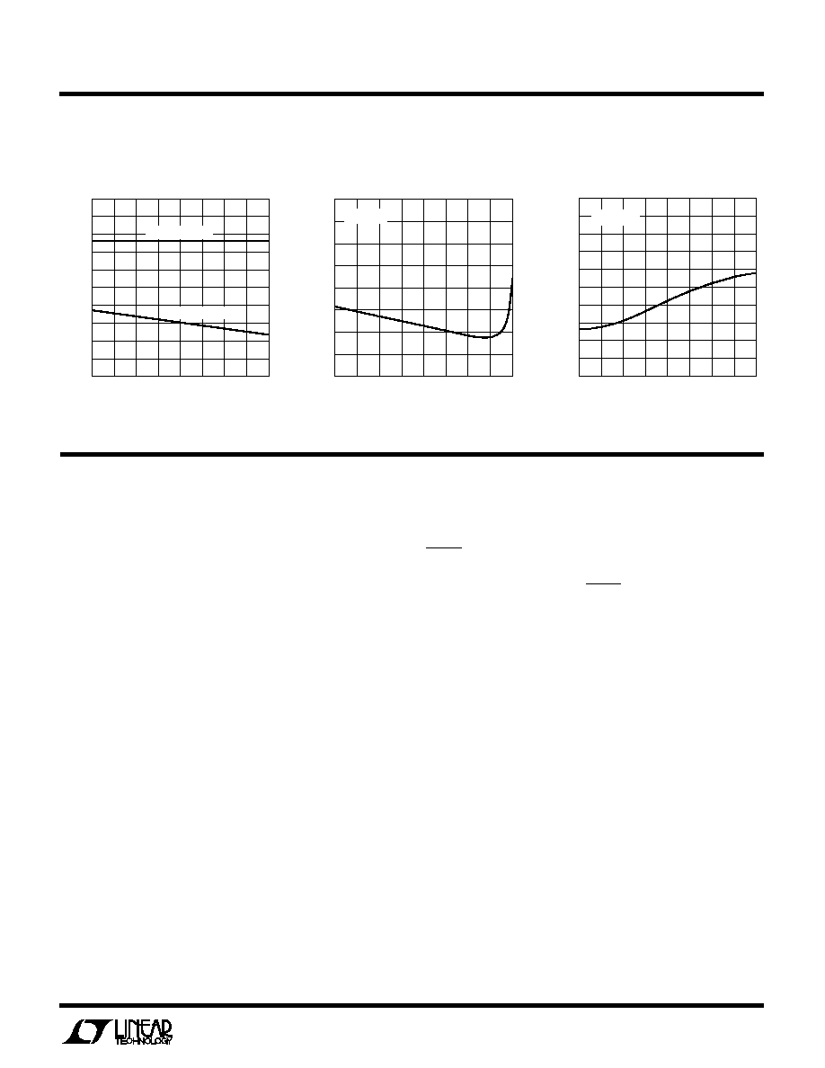
5
LT1371
TYPICAL PERFOR
M
A
N
CE CHARACTERISTICS
U
W
TEMPERATURE (
░
C)
¡50
FEEDBACK INPUT CURRENT (nA)
400
500
600
150
LT1371 À G11
300
200
0
0
50
100
100
800
700
¡25
25
75
125
V
FB
=V
REF
Feedback Input Current
vs Temperature
TEMPERATURE (
░
C)
¡50
¡50
NEGATIVE FEEDBACK INPUT CURRENT (
Á
A)
¡30
0
0
50
75
LT1371 À G12
¡40
¡10
¡20
¡25
25
100 125
150
V
NFB
=V
NFR
Negative Feedback Input Current
vs Temperature
V
C
Pin Threshold and High
Clamp Voltage vs Temperature
TEMPERATURE (
░
C)
¡50
0.4
V
C
PIN VOLTAGE (V)
0.6
1.0
1.2
1.4
2.4
1.8
0
50
75
LT1371 À G10
0.8
2.0
2.2
1.6
¡25
25
100 125
150
V
C
HIGH CLAMP
V
C
THRESHOLD
PI
N
FU
N
CTIO
N
S
U
U
U
V
C
: The Compensation pin is used for frequency compen-
sation, current limiting and soft start. It is the output of the
error amplifier and the input of the current comparator.
Loop frequency compensation can be performed with an
RC network connected from the V
C
pin to ground.
FB: The Feedback pin is used for positive output voltage
sensing and oscillator frequency shifting. It is the invert-
ing input to the error amplifier. The noninverting input of
this amplifier is internally tied to a 1.245V reference. Load
on the FB pin should not exceed 250
Á
A when NFB pin is
used. See Applications Information.
NFB: The Negative Feedback pin is used for negative
output voltage sensing. It is connected to the inverting
input of the negative feedback amplifier through a 100k
source resistor.
S/S (R and T7 Packages Only): Shutdown and Synchroni-
zation Pin. The S/S pin is logic level compatible. Shutdown
is active low and the shutdown threshold is typically 1.3V.
For normal operation, pull the S/S pin high, tie it to V
IN
or
leave it floating. To synchronize switching, drive the S/S
pin between 600kHz and 800kHz.
SHDN: (SW Package Only): The Shutdown pin is active
low and the shutdown threshold is typically 1.3V. For
normal operation, pull the SHDN pin high, tie it to V
IN
or
leave it floating.
SYNC (SW Package Only): To synchronize switching,
drive the SYNC pin between 600kHz and 800kHz. If not
used, the SYNC pin can be tied high, low or left floating.
V
IN
: Bypass Input Supply pin with a low ESR capacitor,
10
Á
F or more. The regulator goes into undervoltage lock-
out when V
IN
drops below 2.5V. Undervoltage lockout
stops switching and pulls the V
C
pin low.
V
SW
: The Switch pin is the collector of the power switch
and has large currents flowing through it. Keep the traces
to the switching components as short as possible to
minimize radiation and voltage spikes.
GND: Tie all Ground pins to a good quality ground plane.