1
LT1036
1036fa
s
Two Regulated Outputs:
12V at 3A
5V at 75mA
s
2% Output Voltage Tolerance
s
60dB Ripple Rejection
s
0.7% Load Regulation
s
TTL and CMOS Compatible Logic Control
s
100% Thermal Burn-In on All Devices
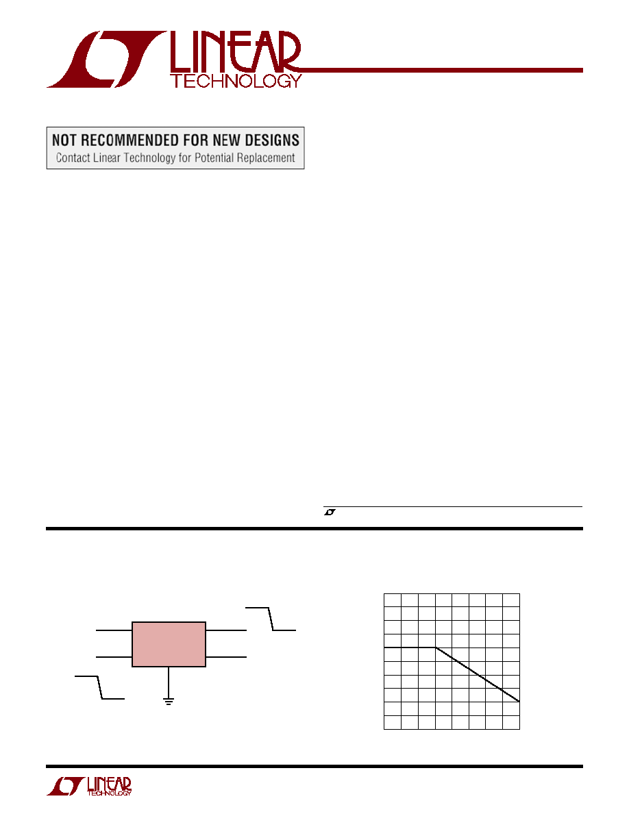
The LT
®
1036 features two positive regulators in the same
package. The 12V main regulator offers excellent
performance while supplying load currents up to 3A, and
the 5V auxiliary regulator provides similar performance
while supplying lighter loads of 75mA. The main regulator
has the additional feature of being under the shutdown
control of a logic signal. When the enable pin is taken to a
low logic level, the main regulator shuts down and its
output voltage goes to near 0V. During this command, the
auxiliary output is unaffected by the main regulator's
condition and continues to provide a 5V output.
The main output has current and power limiting combined
with thermal shutdown to make it virtually blowout proof.
The auxiliary output is not affected by the thermal
shut down mechanism or the state of the main output,
allowing it to be used as a back-up in case of overloads or
shorts on the main supply.
The logic input of the LT1036 (enable pin) has a 1.6V
threshold and can be driven from a high source
impedance. This allows it to be driven by most logic
families, including TTL and CMOS.
For a dual 5V version of the LT1036, please see the LT1035
data sheet.
s
Power Supply Sequencing
s
Remote On/Off Power Control
s
Selective System Power During Emergency
Power Operation
s
Memory Power Supply with Back-Up
Functional Diagram
Logic Controlled Regulator
Guaranteed Load Current,
12V Output
FEATURES
APPLICATIO S
U
DESCRIPTIO
U
, LTC and LT are registered trademarks of Linear Technology Corporation.
TYPICAL APPLICATIO
U
12V
5
2
3
1
4
LOGIC
V
IN
ENABLE
5V
OV
LT1036
GND
OUT
AUX
IN
EN
LT1036M/1036C · FD01
INPUT VOLTAGE (V)
14
0
CURRENT (A)
0.5
1.5
2
2.5
5
3.5
18
22
24
LT1036M/1036C · FD02
1
4
4.5
3
16
20
26
28
30
2
LT1036
1036fa
ORDER PART
NUMBER
LT1036MK
LT1036CK
ORDER PART
NUMBER
LT1036CT
1
4
5
2
V
IN
V
O
V
EN
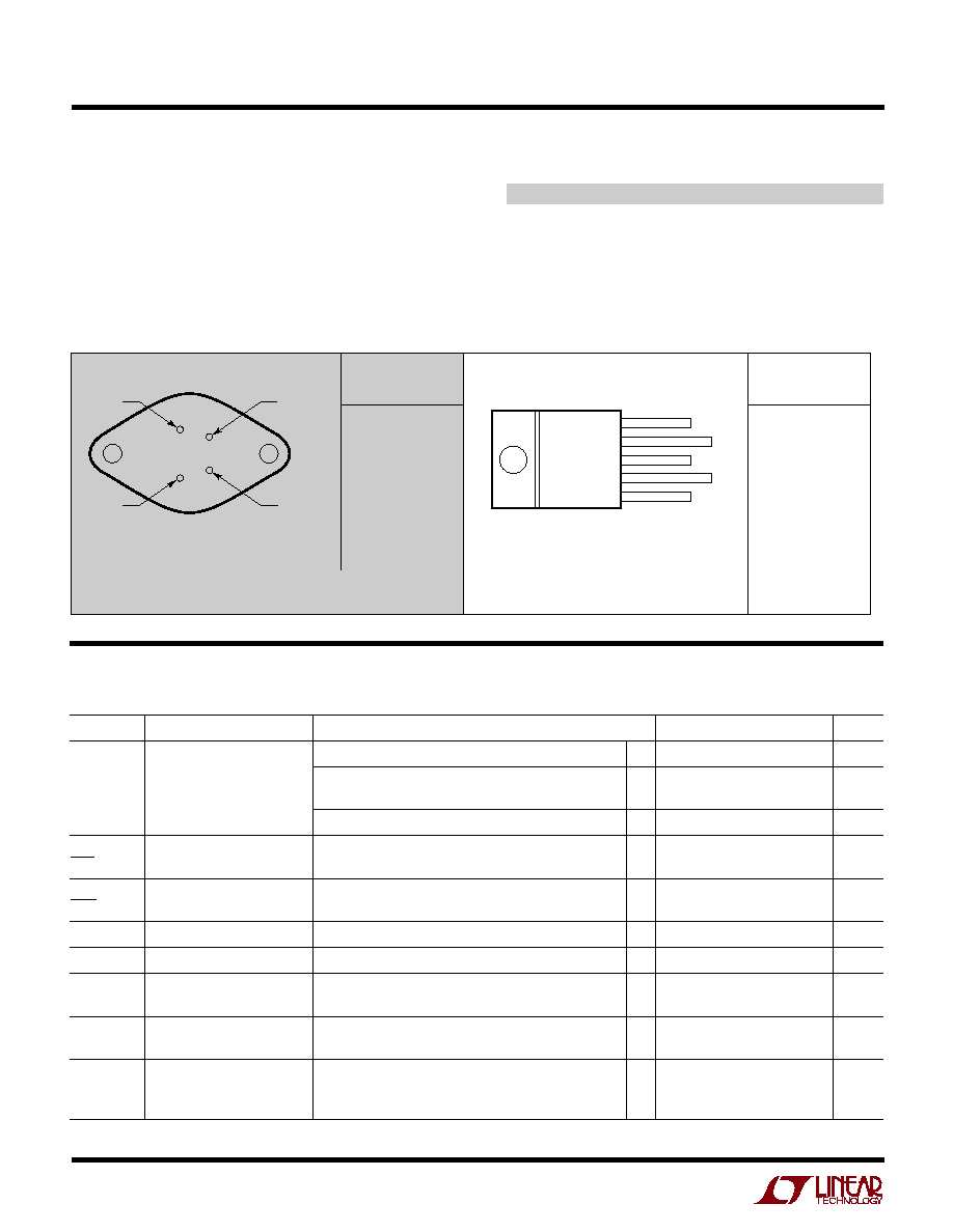
CASE
IS GND
AUX
K PACKAGE
4-LEAD TO-3 METAL CAN
BOTTOM VIEW
T
JMAX
= 125
°
C,
JC
= 3
°
C/W
T PACKAGE
5-LEAD PLASTIC TO-220
FRONT VIEW
V
IN
AUX
GND
V
EN
V
O
5
4
3
2
1
T
JMAX
= 150
°
C,
JC
= 2.5
°
C/W
T
JMAX
= 125
°
C,
JC
= 2.5
°
C/W
Operating Junction Temperature
LT1036M (OBSOLETE) ..................... 55
°
C to 150
°
C
LT1036C ................................................ 0
°
C to 125
°
C
Storage Temperature Range ................. 65
°
C to 150
°
C
Lead Temperature (Soldering, 10 sec).................. 300
°
C
Power Dissipation
Continuous (Note 6) ........................................... 24W
Fault Conditions .............................. Internally Limited
Input Voltage (V
IN
) .................................................. 30V
Enable Voltage (V
EN
) ............................................... 30V
ABSOLUTE AXI U RATI GS
W
W
W
U
ELECTRICAL CHARACTERISTICS
SYMBOL
PARAMETER
CONDITIONS
MIN
TYP
MAX
UNITS
V
O
Output Voltage
T
J
=
25
°
C
11.76
12
12.24
V
High
15V
V
IN
30V,
q
11.52
12.48
V
I
OUT
I
MAX
(Note 7)
Low
7V
V
IN
30V
q
0.1
0.3
V
V
O
Load Regulation
V
IN
=
16V
I
O
(Note 7)
0
I
O
3A (Note 3)
q
10
80
mV
V
O
Line
15V
V
IN
30V
1
4
mV/V
V
IN
Regulation
(Note 3)
Ripple Rejection
50Hz
f
500Hz (Note 9)
50
60
dB
Thermal Regulation
P
D =
20W (Note 5)
0.003
0.012
%/W
I
O
Available Load Current
15V
V
IN
20V
q
3
4
A
(Note 7)
V
IN
= 25V
q
2
2.7
A
I
SC
Short Circuit
V
IN
=
15V
2.3
4
A
Current
V
IN
= 25V
1
2
A
V
IN
Input Voltage to
(Note 6)
Maintain Regulation
I
O
= 1A
q
13.8
14.5
V
(Dropout Voltage)
I
O
= 3A
q
14.4
15
V
PACKAGE/ORDER I FOR ATIO
U
U
W
100% Burn-In in Thermal Limit
PRECO DITIO I G
U
U
U
Consult LTC Marketing for parts specified with wider operating temperature ranges.
The
q
denotes the specifications which apply over the full operating
temperature range. Main regulator (Note 2) V
IN
= 15V unless otherwise noted.
(Note 1)
OBSOLETE PACKAGE
Consider the T Package as an Alternate Source

3
LT1036
1036fa
Note 1: Absolute Maximum Ratings are those values beyond which the life
of a device may be impaired.
Note 2: Unless otherwise indicated, these specifications apply for
V
IN
= 15V, I
O
= 0mA, and T
J
= 25
°
C.
Note 3: Line and load regulation is measured using a low duty cycle pulse,
causing little change in the junction temperature. Effects due to thermal
gradients and device heating must be taken into account separately.
Note 4: When the enable pin is at a low logic level, current flows out of the
enable pin.
SYMBOL
PARAMETER
CONDITIONS
MIN
TYP
MAX
UNITS
V
O
Output Voltage
T
J
=
25
°
C
4.9
5.0
5.1
V
7.2V
V
IN
30V
0mA
I
O
75mA
q
4.8
5.0
5.2
V
V
O
Load
7.2V
V
IN
30V
I
O
Regulation
0mA
I
O
75mA (Note 3)
q
5
15
mV
V
O
Line
7.2V
V
IN
30V
0.2
1
mV/V
V
IN
Regulation
(Note 3)
2
mV/V
Ripple Rejection
50Hz
f
500Hz
74
dB
I
SC
Short Circuit
7.0V
V
IN
30V
140
250
mA
Current (Note 8)
V
IN
Input Voltage to
(Note 6)
Maintain Regulation
I
O
10mA
q
6.2
6.5
V
(Dropout Voltage)
I
O
= 75mA
q
6.8
7.2
V
SYMBOL
PARAMETER
CONDITIONS
MIN
TYP
MAX
UNITS
V
EN
Enable Threshold Voltage
7.0V
V
IN
30V
1.45
1.6
1.7
V
T
J
=
25
°
C
q
1.3
1.6
1.8
V
Enable Pin Current
V
EN
1V (Note 4)
q
0
1.5
12
µ
A
V
EN
2.4V
q
0
6
µ
A
Note 5: Pulse length for this measurement is 20ms.
Note 6: Input voltage is reduced until output drops by 100mV from its
initial value.
Note 7: See "Guaranteed Load Current" graph.
Note 8: Continuous shorts on the auxiliary output are not allowed unless
adequate heat sinking is used to maintain junction temperature below
150
°
C.
Note 9: Guaranteed but not tested.
Logic Control (Note 2)
ELECTRICAL CHARACTERISTICS
SYMBOL
PARAMETER
CONDITIONS
MIN
TYP
MAX
UNITS
I
Q
Quiescent
Output High
4
5.5
mA
Current
Output Low
3
4.5
mA
JC
Thermal Resistance,
TO-220
2
3
°
C/W
Junction to Case
The
q
denotes the specifications which apply over the full operating
temperature range. Main Regulator (Note 2) V
IN
= 15V unless otherwise noted.
Auxiliary Regulator (Note 2)

4
LT1036
1036fa
TYPICAL PERFOR A CE CHARACTERISTICS
U
W
Minimum Input-Output
Differential of Main Output
Line Transient Response,
12V Output
Minimum Input-Output
Differential of Auxiliary Output
OUTPUT CURRENT (mA)
0
INPUT-OUTPUT VOLTAGE (V)
1.8
2.2
2.6
2.4
80
LT1036M/1036C · TPC02
1.4
1.0
1.6
2.0
1.2
0.8
0.6
20
40
60
100
T
J
= 55
°
C
T
J
= 150
°
C
T
J
= 25
°
C
ENABLE VOLTAGE (V)*
0
CURRENT (
µ
A)
0.6
0.2
2.0
LT1036M/1036C · TPC08
1.0
1.4
0.8
0.4
0
1.2
1.6
1.8
1.4
1.3
*NOTE SCALE CHANGE
1.6
1.5
1.8 1.9
2.1
1.7
20
T
J
= 25
°
C
JUNCTION TEMPERATURE (
°
C)
50
THRESHOLD (V)
1.55
1.65
150
LT1036M/1036C · TPC09
1.45
1.35
0
50
100
25
25
75
125
1.75
1.50
1.60
1.40
1.70
Load Transient Response,
12V Output
Enable Threshold
Enable Pin Characteristics
Maximum Available Load
Current, 12V Output
Output Voltage vs Temperature
Quiescent Current
OUTPUT CURRENT (A)
0
INPUT-OUTPUT VOLTAGE (V)
1.6
1.8
2.0
1.5
2.5
LT1036M/1036C · TPC01
1.4
1.2
1.0
0.5
1.0
2.0
2.2
2.4
2.6
3.0
T
J
= 55
°
C
T
J
= 25
°
C
T
J
= 150
°
C
INPUT VOLTAGE (V)
0
0
CURRENT (A)
2
5
8
16
20
LT1036M/1036C · TPC04
1
4
3
4
12
24
28
32
DEVICE OUT OF REGULATION
BELOW 14V
T
J
= 25
°
C
INPUT VOLTAGE (V)
0
SUPPLY CURRENT (mA)
8
7
6
5
4
3
2
1
0
24
LT1036M/1036C · TPC05
6
12
18
30
21
3
9
15
27
T
J
= 25
°
C
12V OUTPUT "ON"
12V OUTPUT "OFF"
TEMPERATURE (
°
C)
50
4.7
MAIN OUTPUT (V)
AUXILIARY OUTPUT (V)
4.8
5.0
5.1
12.2
11.9
0
50
75
LT1036M/1036C · TPC06
4.9
12.0
12.1
11.8
25
25
100 125
150
TIME (
µ
s)
OUTPUT VOLTAGES
CHANGE (V)
LOAD
TRANSIENT (A)
0.2
50
50
50
2
6
8
LT1036M/1036C · TPC07
0
50
0
0
0
4
10
12
14
C
OUT
= 1
µ
F TANTALUM
C
OUT
= 10
µ
F TANTALUM
LOAD TRANSIENT
I
OUT
= 1A
I
OUT
= 0.2A
TIME (
µ
s)
OUTPUT
VOLTAGE CHANGE (mV)
INPUT
TRANSIENT (V)
1
20
0
20
2
6
8
LT1036M/1036C · TPC03
0
0
20
20
0
4
10
12
14
C
OUT
= 1
µ
F TANTALUM
C
OUT
= 10
µ
F TANTALUM
V
IN
= 1V
V
IN
= 18V

5
LT1036
1036fa
TYPICAL PERFOR A CE CHARACTERISTICS
U
W
Short-Circuit Current, 12V Output
Output Voltage Noise
Output Switching Characteristics
INPUT VOLTAGE (V)
0
0
CURRENT (A)
2
5
8
16
20
LT1036M/1036C · TPC10
1
4
3
4
12
24
28
32
T
J
= 25
°
C
General Information
The LT1036 is a dual output regulator. The main 12V
output is capable of delivering up to 3A of load current and
can be shut down with a logic signal. The auxiliary 5V
output supplies a minimum of 75mA and is unaffected by
the logic signal. The outputs are trimmed to
±
2% initial
tolerance and exhibit excellent line and load regulation.
The logic control feature makes the LT1036 ideal for many
system applications where it is desirable to power-up a
portion of the system for a period of time, and then power
the system down during a standby operation. Applications
such as multiple power supply sequencing, elimination of
expensive AC and DC power switches, delayed start ap-
plications, switching 12V DC loads, and many others are
now easily accomplished.
Timing functions, such as delayed power-up or power-
down, can also be performed directly at the enable pin.
Because a logic low on the enable pin shuts down the main
regulator, feedback from output to enable can be used to
generate hysteresis or latching functions.
APPLICATIO S I FOR ATIO
W
U
U
U
The low quiescent current drain of the LT1036 makes it
useful in battery-powered or battery back-up applications.
The enable pin can be used as a "low battery" detector or
to shut down major portions of system power, allowing
memory portions to continue to operate from the auxiliary
output. At low output currents, the auxiliary output will
regulate with input voltage typically as low as 6.2V, giving
maximum battery life.
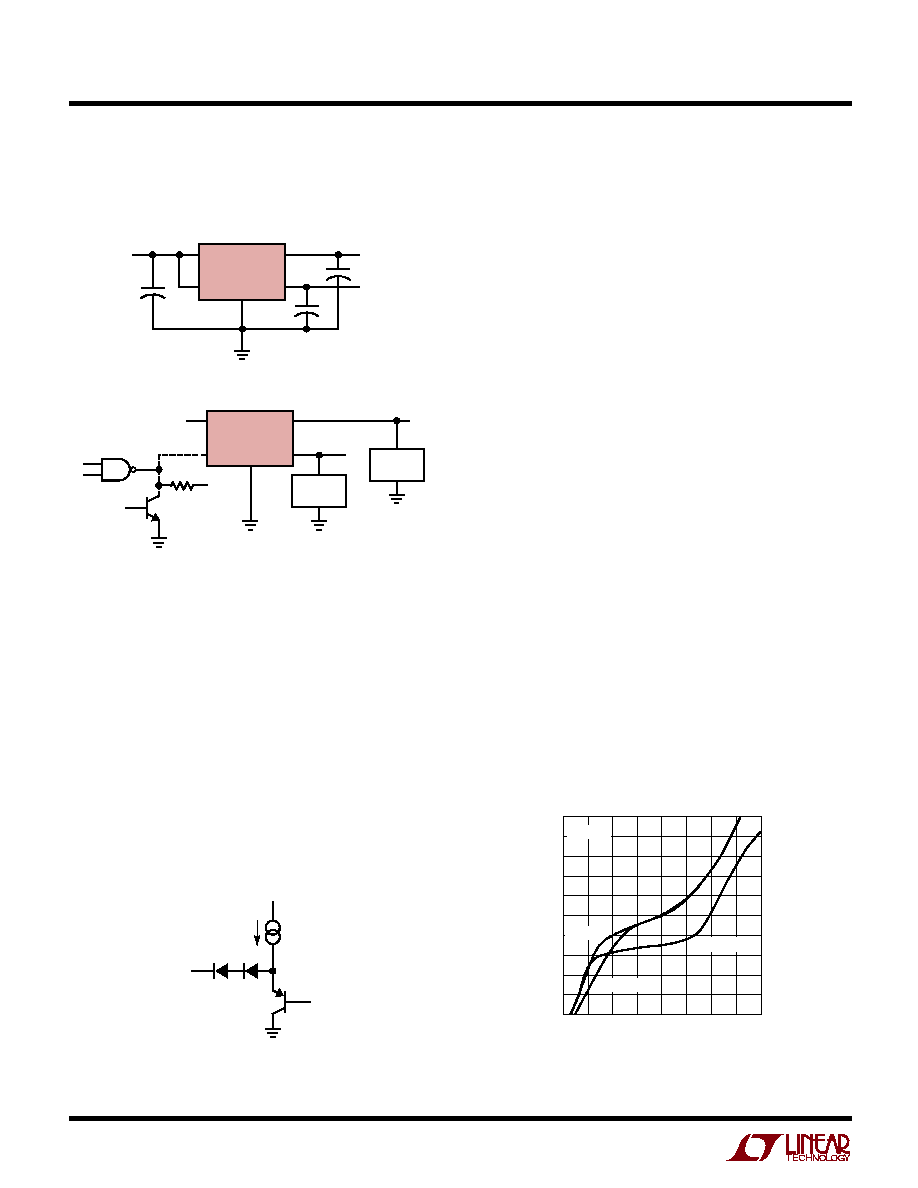
Good design practice with all regulators is to bypass the
input and output terminals. A 2
µ
F solid tantalum at the
input and at both outputs is suggested. For the applica-
tions which follow, the bypass capacitors are still recom-
mended, but for simplicity are not shown on the diagram.
It is also recommended that for maximum noise immunity
the voltage enable pin be tied high if it is unused. It can be
tied directly to V
IN
, as shown in Figure 1, or to the auxiliary
Output. If the enable pin is left open, it will float to a high
logic level of approximately 1.6V and the main output
regulator will be at 12V.
The enable pin is fully protected against input voltages up
to 30V, even if the power input voltage is zero.
TIME (
µ
s)
OUTPUT VOLTAGE (V)
ENABLE
VOLTAGE (V)
15
12
9
6
3
0
5
0
70
LT1036M/1036C · TPC11
10
30
50
90
60
0
20
40
80
C
OUT
0.1F
C
OUT
0.1
µ
F
C
OUT
= 1
µ
F
C
OUT
= 10
µ
F
SEE APPLICATION SECTION
FOR FALL TIME INFORMATION
BANDWIDTH (1 POLE) (Hz)
100
NOISE (
µ
V
RMS
)
120
160
200
10k
LT1036M/1036C · TPC12
80
40
100
140
180
60
20
0
300
1k
3k
30k
MAIN (12V) OUTPUT
AUXILIARY
OUTPUT
6
LT1036
1036fa
Figure 1
Figure 2
Figure 3
The basic shutdown control circuit uses a direct gate drive
or an open collector driver and a pull-up resistor which are
tied to V
AUX
, as shown in Figure 2.
APPLICATIO S I FOR ATIO
W
U
U
U
Driving the Enable Pin
The enable pin equivalent schematic is shown in Figure 3.
Basically, enable pin current is zero above the threshold
and about 1.5
µ
A below the threshold, flowing out of the
pin. Standard logic, such as TTL and CMOS, will interface
directly to the enable pin, even if the logic output swing is
higher than the input voltage (V
IN
) to the regulator.
15V CMOS can be used to drive the enable pin, even if
the regulator is not powered up, without loading the
CMOS output.
Timing functions, such as delayed power-up or
power-down can be implemented with an RC network.
The current flowing out of the enable pin should not
be used as the timing current in delayed power-up
applications as it is temperature sensitive and varies
somewhat from device to device. Instead, a resistor tied to
the auxiliary output, the input, or to a logic signal should
be used. The timing resistor chosen should provide at
least 25
µ
A of current to "swamp out" the effects of the
internal current.
Main Output Current Voltage Characteristics
Following a high to low transition at the enable pin, the
main regulator output will begin to drop after a delay of
approximately 0.4
µ
s. With no capacitive load, the output
will fall to zero in approximately 0.8
µ
s (R
L
= 4
to 100
).
With a capacitive load, fall time is limited by the RC product
of the load and the output capacitance. For light loads
(R
L
>400
), the discharge time is controlled by an
internal current pull-down of 15mA for output voltages
down to 1.5V. Below 1.5V, the pull-down current drops to
4mA. The DC output voltage in the shutdown mode is
approximately 0.12V due to an internal current path in the
regulator. (See Figure 4.)
The user should note that the output in the low state can
only sink about 3mA. If current is forced into the output,
the output voltage will rise to 1V at 5mA and about 1.5V at
10mA. With no output capacitor, the rise time of the main
output is about 12
µ
s. With an output capacitor, rise time
is limited by the short circuit current of the LT1036 and the
load capacitance. A 10
µ
F output capacitor slows the
output rise time to approximately 80
µ
s.
Figure 4
V
IN
V
O
12V
5V
+
+
+
LT1036
GND
OUT
IN
1
4
3
2
5
AUX
EN
1
µ
F
2
µ
F
2
µ
F
LT1036M/1036C · AI01
7.5-20V
12V
5V
V
AUX
LT1036
GND
OUT
IN
AUX
EN
LT1036M/1036C · AI02
0mA75mA
LOAD
0A-3A
LOAD
OUTPUT VOLTAGE (V)
0
0
CURRENT FORCED INTO OUTPUT (mA)
1
3
4
5
10
7
0.4
0.8
1.0
LT1036M/1036C · AI04
2
8
9
6
0.2
0.6
1.2
1.4
1.6
T
J
= 25
°
C
T
J
= 150
°
C
T
J
= 55
°
C
V
IN
= 15V
ENABLE
1V
70
µ
A
LT1036M/1036C · AI03

7
LT1036
1036fa
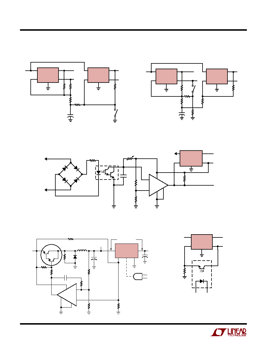
Fast Turn-Off, Delayed Turn-On
APPLICATIO S I FOR ATIO
W
U
U
U
Output Current
The main output current limits at about 4A for input
voltages below 20V. Internal foldback, or "power limit-
ing", circuitry detects the input-output voltage differential
and reduces current limit for input to output voltages
exceeding 8V. With 25V input, for instance, short circuit
current is reduced to
0.9A.
An additional feature of the LT1036 is that the auxiliary
supply does not incorporate, nor is it affected by, thermal
shutdown. Any fault condition of the main regulator will
not affect the auxiliary output voltage.
The following applications circuits will serve to indicate
the versatility of the LT1036.
TYPICAL APPLICATIO S
U
Latch-Off with Output Short
Delayed Power-Up
Thermal Cutoff at High Ambient Temperature
Power Supply Turn-On Sequencing
12V
LT1036M/1036C · TA01
+
LT1036
GND
OUT
IN
AUX
t
ON
= 0.3 R1C1
R1
100k
EN
C1
V
IN
*CAN BE ANY GATE TYPE
*
LT1036M/1036C · TA02
12V
5V
LT1036
GND
OUT
IN
AUX
EN
V
IN
68k
0.33
µ
F
LT1036M/1036C · TA03
12V
5V
t
DELAY
0.4 R1C1
R1
27k
LT1036
GND
OUT
IN
AUX
EN
V
IN
C1
LT1036M/1036C · TA04
LT1036
GND
OUT
IN
AUX
26.1k
t
OFF
= 58
°
C
t
ON
= 46
°
C
154k
R
t
*
EN
5V
V
IN
*YELLOW SPRINGS #44008. 30k
at 25
°
C
LT1036
GND
OUT
IN
AUX
t
1
= 0.4 R1C1
t
2
=
0.15 R2C2
R1
EN
LT1036
GND
OUT
IN
AUX
EN
C1
V
IN
LT1036M/1036C · TA05
R2
C2
8
LT1036
1036fa
TYPICAL APPLICATIO S
U
First-On, Last-Off Sequencing
First-On, First-Off Sequencing
LT1036
"FIRST ON"
GND
OUT
IN
AUX
R4
150k
t
ON
(1) = 50ms
t
ON
(2) = 150ms
50
µ
F
R1
10k
EN
R5
150k
LT1036
GND
OUT
IN
AUX
EN
R2
2.2k
R3
1k
12V
5V
OFF
ON
12V
V
IN
5V
LT1036M/1036C · TA06
+
LT1036
"FIRST ON"
GND
OUT
IN
AUX
t
ON
(1) = 100ms
t
ON
(2) = 200ms
100
µ
F
EN
R6
150k
LT1036
GND
OUT
IN
AUX
EN
R3
1k
R5
1k
R1
1k
R2
4.7k
12V
5V
OFF
ON
12V
V
IN
5V
LT1036M/1036C · TA07
R4
150k
+
Low Dissipation Regulator
Optocoupled Output Control
LT1036M/1036C · TA10
12V
5V
LT1036
GND
OUT
IN
AUX
EN
V
IN
R
COUPLER "ON" = OUTPUT "ON"
SELECT R DEPENDING UPON THE
ON-RESITANCE OF THE OPTOCOUPLER
3.9k
27k
2N6667
1mH*
15.5V
LT1035
6000
µ
F
OUTPUT
CONTROL
LOGIC
*DALE TD-5
THIS CIRCUIT IS DESIGNED TO
REDUCE POWER DISSIPATION
IN THE LT1036 OVER A
90VAC140VAC INPUT RANGE
V
IN
17.5VDC
TO 30VDC
1000pF
1k
8
2
3
4
1
7
1k
1N4003
150k
10.5k
5k
5k
+
AUX
4
2
3
1
5
EN
LT1036
LT1011
COMPARATOR
GND
V
OUT
V
IN
10
µ
F
12V
OUTPUT
3.5V DC UNDER
ALL CONDITIONS
LT1036M/1036C · TA09
+
+
Line Dropout Detector
LT1036M/1036C · TA08
LT1036
GND
3.3k
TO FILTERED
RAW DC
5V AUXILIARY
DROPOUT
SIGNAL
12V
1
4
8
OUT
IN
AUX
EN
7
3
2
+
LT1011
2k
0.1
µ
F
3k
18k
TRIP SET
500k
4N46
1N4148(4)
TO SECONDARY
OF AC POWER
TRANSFORMER
9
LT1036
1036fa
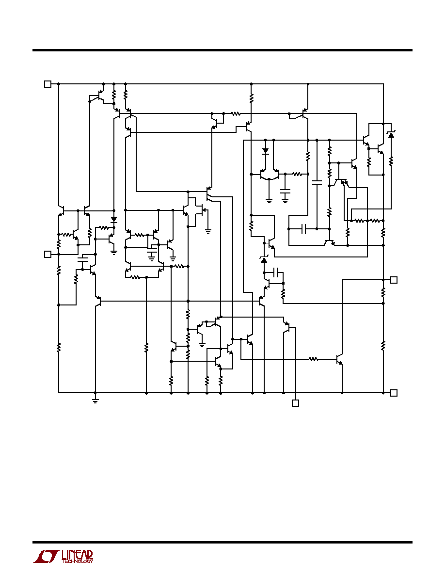
SCHE ATIC DIAGRA
W
W
2k
LT1036M/1036C · SD01
800
V
IN
860
Q38
Q37
Q1
Q2
Q3
Q5
Q12
Q13
Q34
Q35
Q36
5
4
AUX
OUTPUT
2
ENABLE
3
GND
1
MAIN
OUTPUT
4
4k
10k
12k
20.4k
5k
8k
900
1.2k
500
D5
20
20pF
Q9
Q14
Q11
Q10
Q4
Q7
Q6
Q8
100k
10k
2.9k
2.1k
7k
500
Q15
Q16
Q17
Q18
Q33
3k
5k
Q32
Q23
Q24
D1
Q31
6k
Q19
1.3k
D3
6.5V
2k
10k
8k
750
115
0.03
4.8k
2k
3k
430
5k
15pF
30
pF
10pF
Q21
8k
Q22
Q20
Q28
Q27
Q26
Q29
D2
7V
20pF
400
50
Q39
Q30
Q25
10
LT1036
1036fa
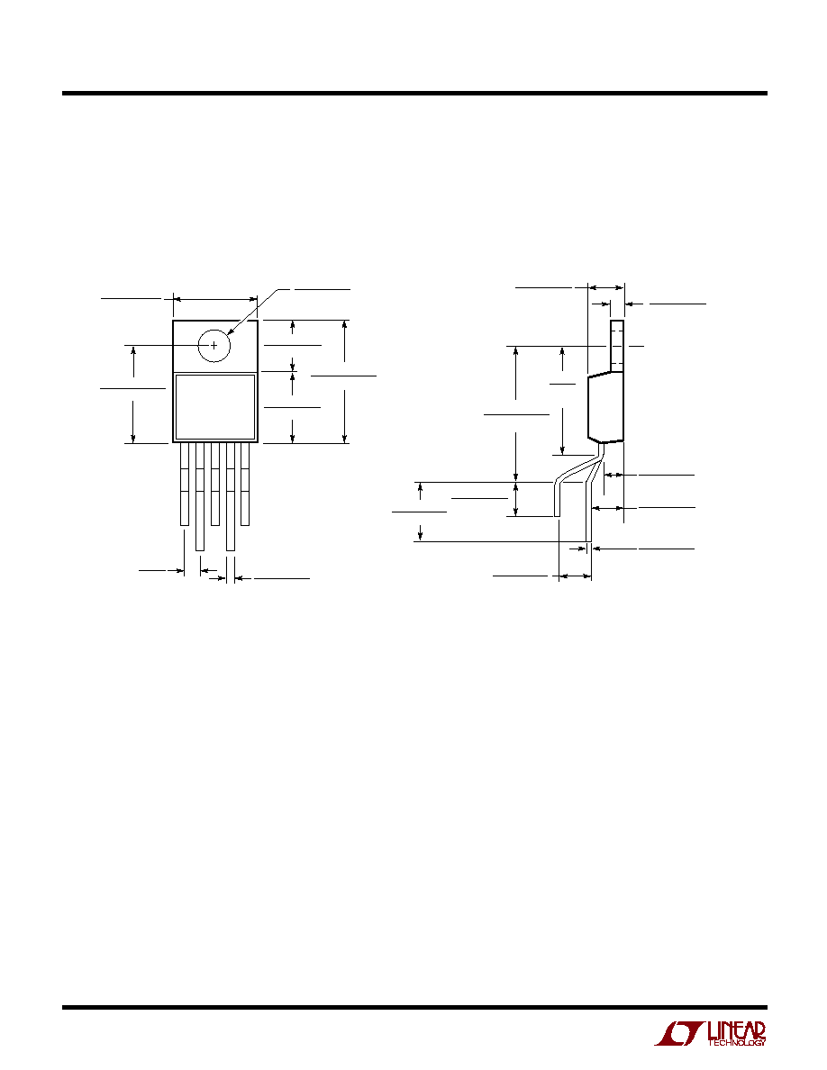
T Package
5-Lead Plastic TO-220 (Standard)
(Reference LTC DWG # 05-08-1421)
T5 (TO-220) 0399
0.028 0.038
(0.711 0.965)
0.067
(1.70)
0.135 0.165
(3.429 4.191)
0.700 0.728
(17.78 18.491)
0.045 0.055
(1.143 1.397)
0.095 0.115
(2.413 2.921)
0.013 0.023
(0.330 0.584)
0.620
(15.75)
TYP
0.155 0.195*
(3.937 4.953)
0.152 0.202
(3.861 5.131)
0.260 0.320
(6.60 8.13)
0.165 0.180
(4.191 4.572)
0.147 0.155
(3.734 3.937)
DIA
0.390 0.415
(9.906 10.541)
0.330 0.370
(8.382 9.398)
0.460 0.500
(11.684 12.700)
0.570 0.620
(14.478 15.748)
0.230 0.270
(5.842 6.858)
BSC
SEATING PLANE
* MEASURED AT THE SEATING PLANE
U
PACKAGE DESCRIPTIO
11
LT1036
1036fa
Information furnished by Linear Technology Corporation is believed to be accurate and reliable.
However, no responsibility is assumed for its use. Linear Technology Corporation makes no represen-
tation that the interconnection of its circuits as described herein will not infringe on existing patent rights.
U
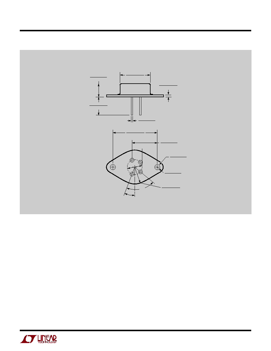
PACKAGE DESCRIPTIO
K4(TO-3) 1098
72
°
18
°
0.490 0.510
(12.45 12.95)
R
0.470 TP
P.C.D.
0.167 0.177
(4.24 4.49)
R
0.151 0.161
(3.84 4.09)
DIA 2 PLC
0.655 0.675
(16.64 19.05)
1.177 1.197
(29.90 30.40)
0.038 0.043
(0.965 1.09)
0.060 0.135
(1.524 3.429)
0.320 0.350
(8.13 8.89)
0.420 0.480
(10.67 12.19)
0.760 0.775
(19.30 19.69)
OBSOLETE PACKAGE
K Package
4-Lead TO-3 Metal Can
(Reference LTC DWG # 05-08-1311)
12
LT1036
1036fa
Linear Technology Corporation
1630 McCarthy Blvd., Milpitas, CA 95035-7417
(408) 432-1900
q
FAX: (408) 434-0507
q
www.linear.com
LW/TP 0902 1K REV A · PRINTED IN USA
©
LINEAR TECHNOLOGY CORPORATION 1985
PART NUMBER
DESCRIPTION
COMMENTS
LT1573
UltraFast Transient Response Low Dropout Regulator
V
IN
=2.8 to 10V, V
OUT
= 1.265V, Dropout Voltage = 350mV-Ext PNP
PNP Driver, Up to 5A
V@I
OUT
, I
Q
= 1.7mA, Shutdown Current = 200
µ
A, S8 Package.
Requires External PNP Transistor.
LT1764/A
3A, Low Noise, Fast Transient Response, LDO
V
IN
= 2.7 to 20V, V
OUT
= 1.21V,
Dropout Voltage = .34V@I
OUT
,
I
Q
= 1mA, Shutdown Current < 1
µ
A, DD, TO220-5 Packages. Low
Noise < 40
µ
V
RMS PK-PK.
"A" Version Stable with Ceramic Capacitors.
LT3150
Fast Transient Response Low Dropout Regulator
V
IN
= 1.4 to 10V, V
OUT
= 1.23V,
Dropout Voltage = 150mV Ext FET
MOSFET Driver, Up to 10A
@I
OUT
, I
Q
= 12mA, GN-16 Package. Intgr LT1613 Boost, Drives Low
Cost N-Channel MOSFETs, Fast Transient Response.
RELATED PARTS