PT60QHx45
1/6
APPLICATIONS
q
Pulse Power
q
Crowbars
q
Ignitron Replacement
FEATURES
q
Double Side Cooling
q
Fast Turn-on
q
Low Turn-on Losses
VOLTAGE RATINGS
KEY PARAMETERS
V
DRM
4500V
I
T(AV)
1000A
I
TSM
22500A
dI/dt
10,000A/
µ
s
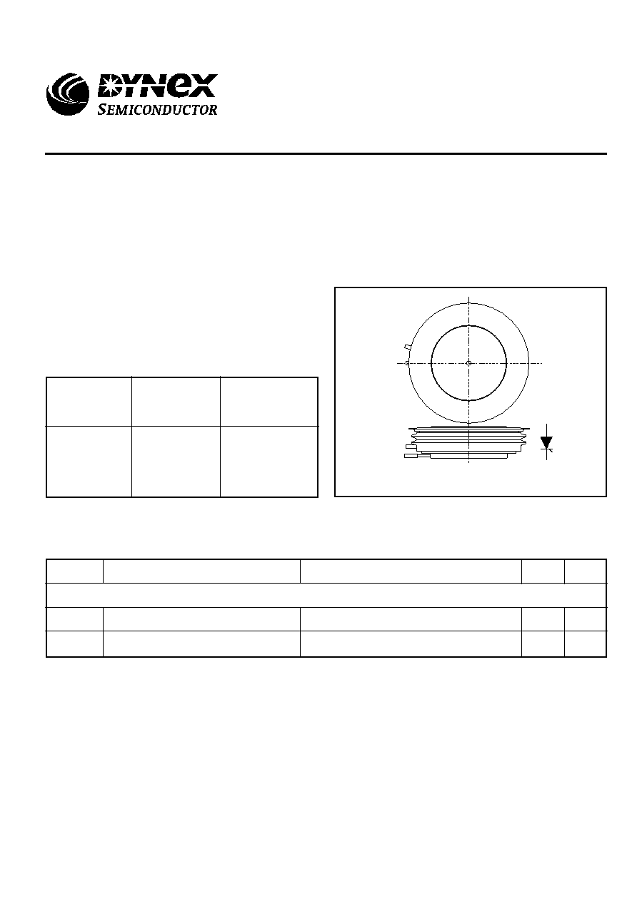
Outline type code: H.
See Package Details for further information.
PT60QHx45
Conditions
T
vj
= 0° to 125°C,
I
DRM
= I
RRM
= 100mA,
V
DRM
, V
RRM
t
p
= 10ms
Lower voltage grades available.
Type Number
Repetitive Peak
Voltages
V
DRM
/V
RRM
V
CURRENT RATINGS
Symbol
Parameter
Conditions
Double Side Cooled
I
T(AV)
Mean on-state current
I
T(RMS)
RMS value
Units
Max.
Half wave resistive load, T
case
= 80
o
C
1000
A
T
case
= 80
o
C
1570
A
4500/16
Fig.1 Package outline
PT60QHx45
Pulse Power Thyristor Switch
Preliminary Information
Replaces February 2000 version, DS5267-1.3
DS5267-1.4 April 2000

PT60QHx45
2/6
Clamping force 19.5kN
with mounting compound
Thermal resistance - case to heatsink
R
th(c-h)
0.003
Double side
-
o
C/W
SURGE RATINGS
Conditions
10ms half sine; T
case
= 125
o
C
V
R
= 50% V
RRM
- 1/4 sine
10ms half sine; T
case
= 125
o
C
V
R
= 0
Max.
Units
Symbol
Parameter
I
TSM
Surge (non-repetitive) on-state current
I
2
t
I
2
t for fusing
I
TSM
Surge (non-repetitive) on-state current
I
2
t
I
2
t for fusing
2.52 x 10
6
A
2
s
22.5
kA
15.8 x 10
6
A
2
s
17.8
kA
THERMAL AND MECHANICAL DATA
dc
Conditions
Min.
Max.
Units
125
o
C
T
vj
Virtual junction temperature
T
stg
Storage temperature range
Reverse (blocking)
-
Thermal resistance - junction to case
R
th(j-c)
Symbol
Parameter
Clamping force
18
22
kN
55
125
o
C
-
On-state (conducting)
-
135
o
C
Double side cooled
-
0.013
o
C/W
DYNAMIC CHARACTERISTICS
Parameter
Symbol
Conditions
Typ.
Max.
Units
I
RRM
/I
DRM
Peak reverse and off-state current
At V
RRM
/V
DRM
, T
case
= 125
o
C
From 67% V
DRM
to 40kA
Gate source 60A
t
r
= 1.5
µ
s to 1A, T
j
= 25
o
C
dV/dt
Maximum linear rate of rise of off-state voltage
To 67% V
DRM
T
j
= 125
o
C. R
gk
1.5
-
100
mA
-
175
V/
µ
s
Non-repetitive
-
10000
A/
µ
s
Rate of rise of on-state current
dI/dt
V
T(TO)
Threshold voltage
At T
vj
= 125
o
C
r
T
On-state slope resistance
At T
vj
= 125
o
C
1.5
-
V
-
0.67
m
GATE TRIGGER CHARACTERISTICS AND RATINGS
V
DRM
= 5V, T
case
= 25
o
C
Conditions
Parameter
Symbol
V
GT
Gate trigger voltage
V
DRM
= 5V, T
case
= 25
o
C
I
GT
Gate trigger current
1.0
V
3
A
Max.
Units
-
-
Typ.

PT60QHx45
3/6
CURVES
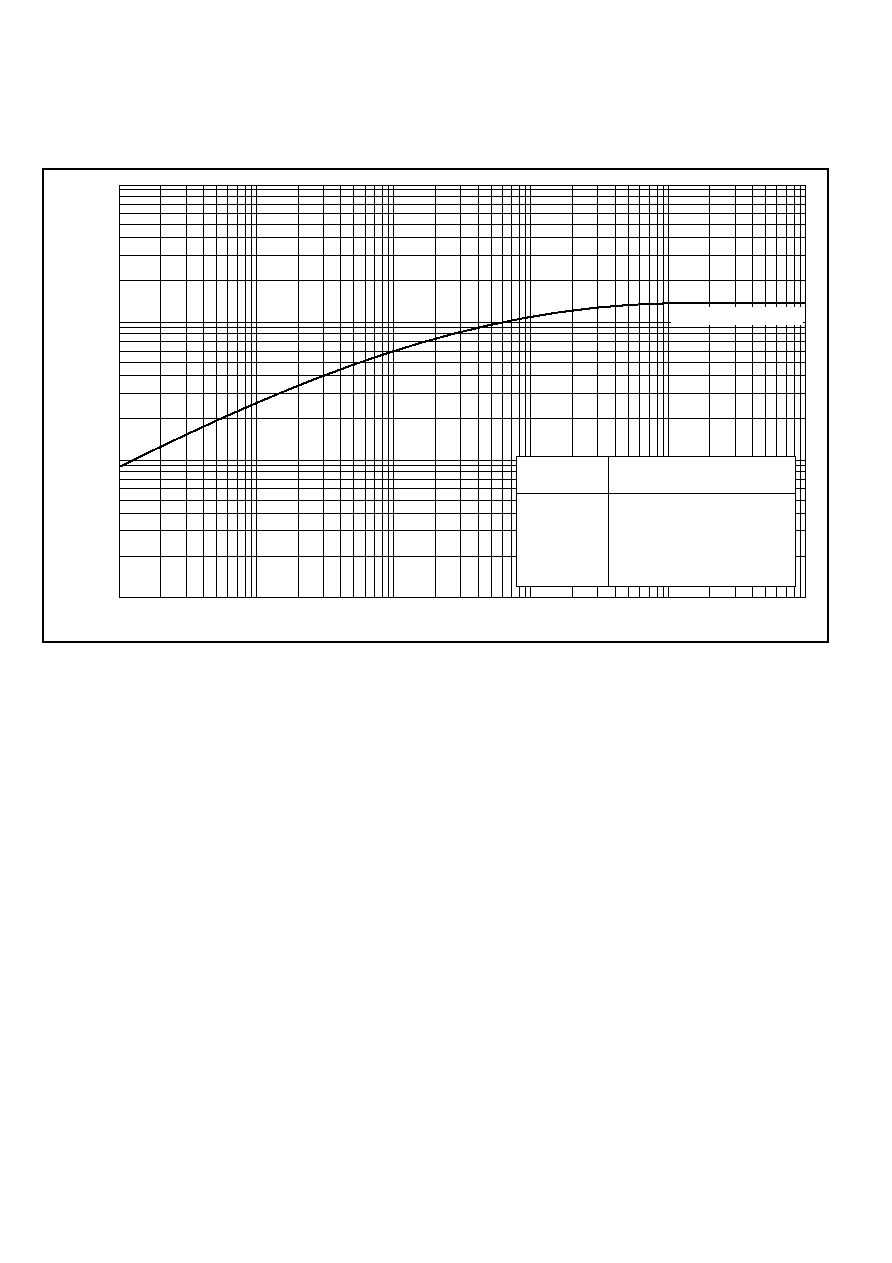
Fig.2 Maximum (limit) on-state characteristics
ORDERING INFORMATION
PT
Pulse Power Thyristor
40Q Device type
P
Package outline type code
x
lead length (see table, right)
45
Voltage x100
Lead length (x)
O
C
D
E
F
G
H
J
K
L
No lead
8"
10"
12"
16"
18"
20"
24"
30"
40"
200mm
250mm
300mm
400mm
450mm
500mm
600mm
750mm
1000mm
1.0
2.0
3.0
4.0
5.0
Instantaneous on-state voltage, V
T
- (V)
0
1000
2000
3000
4000
5000
Measured under pulse conditions
Instantaneous on-state current, I
T
- (A)
1
2
1: T
j
= 25°C Max
2: T
j
= 125°C Max
PT60QHx45
4/6
10
1
0.1
0.01
0.001
Time - (s)
0.1
0.01
0.001
0.0001
Thermal impedance - (°C/W)
Conduction
d.c.
Halfwave
3 phase 120°
6 phase 60°
Effective thermal resistance
Junction to case °C/W
Double side
0.0130
0.0141
0.0170
0.0200
Double side cooled
100
Fig.3 Maximum (limit) transient thermal impedance - junction to case

PT60QHx45
5/6
Package Details
For further package information, please contact your local Customer Service Centre. All dimensions in mm, unless stated otherwise.
DO NOT SCALE.
2 holes Ř3.60
±
0.05 x 2.0
±
0.1 deep (One in each electrode)
26
±
0.5
52
55
9.6
15°
Cathode Aux. Tube
Gate Tube
Cathode
Anode
Ř62.85
Ř100
Ř62.85
Nominal weight: 820g
Clamping force: 20kN
±
10%
Package outine type code: H