PT40QPx45
1/6
APPLICATIONS
q
Pulse Power
q
Crowbars
q
Ignitron Replacement
FEATURES
q
Double Side Cooling
q
Fast Turn-on
q
Low Turn-on Losses
VOLTAGE RATINGS
KEY PARAMETERS
V
DRM
4500V
I
T(AV)
760A
I
TSM
13000A
dI/dt
5000A/
µ
s
Outline type code: P.
See Package Details for further information.
PT40QPx45
Conditions
T
vj
= 0° to 125°C,
I
DRM
= I
RRM
= 50mA,
V
DRM
, V
RRM
t
p
= 10ms
Lower voltage grades available.
Type Number
Repetitive Peak
Voltages
V
DRM
/V
RRM
V
CURRENT RATINGS
Symbol
Parameter
Conditions
Double Side Cooled
I
T(AV)
Mean on-state current
I
T(RMS)
RMS value
Units
Max.
Half wave resistive load, T
case
= 80
o
C
760
A
T
case
= 80
o
C
1190
A
4500/16
Fig.1 Package outline
PT40QPx45
Pulse Power Thyristor Switch
Preliminary Information
Replaces November 1999 version, DS5267-1.1
DS5267-1.4 April 2000

PT40QPx45
2/6
Clamping force 12.0kN
with mounting compound
Thermal resistance - case to heatsink
R
th(c-h)
0.008
Double side
-
o
C/W
SURGE RATINGS
Conditions
10ms half sine; T
case
= 125
o
C
V
R
= 50% V
RRM
- 1/4 sine
10ms half sine; T
case
= 125
o
C
V
R
= 0
Max.
Units
Symbol
Parameter
I
TSM
Surge (non-repetitive) on-state current
I
2
t
I
2
t for fusing
I
TSM
Surge (non-repetitive) on-state current
I
2
t
I
2
t for fusing
845 x 10
3
A
2
s
13.0
kA
541 x 10
3
A
2
s
10.4
kA
THERMAL AND MECHANICAL DATA
dc
Conditions
Min.
Max.
Units
125
o
C
T
vj
Virtual junction temperature
T
stg
Storage temperature range
Reverse (blocking)
-
Thermal resistance - junction to case
R
th(j-c)
Symbol
Parameter
Clamping force
11.0
15.0
kN
55
125
o
C
-
On-state (conducting)
-
135
o
C
Double side cooled
-
0.033
o
C/W
DYNAMIC CHARACTERISTICS
Parameter
Symbol
Conditions
Typ.
Max.
Units
I
RRM
/I
DRM
Peak reverse and off-state current
At V
RRM
/V
DRM
, T
case
= 125
o
C
From 67% V
DRM
to 20kA
Gate source 30A
t
r
= 1.5
µ
s, T
j
= 25
o
C
dV/dt
Maximum linear rate of rise of off-state voltage
To 67% V
DRM
T
j
= 125
o
C. R
gk
1.5
-
50
mA
-
200
V/
µ
s
Non-repetitive
-
5000
A/
µ
s
Rate of rise of on-state current
dI/dt
V
T(TO)
Threshold voltage
At T
vj
= 125
o
C
r
T
On-state slope resistance
At T
vj
= 125
o
C
1.4
-
V
-
0.152
m
GATE TRIGGER CHARACTERISTICS AND RATINGS
V
DRM
= 5V, T
case
= 25
o
C
Conditions
Parameter
Symbol
V
GT
Gate trigger voltage
V
DRM
= 5V, T
case
= 25
o
C
I
GT
Gate trigger current
4.0
V
1.5
A
Max.
Units
1.0
-
Typ.

PT40QPx45
3/6
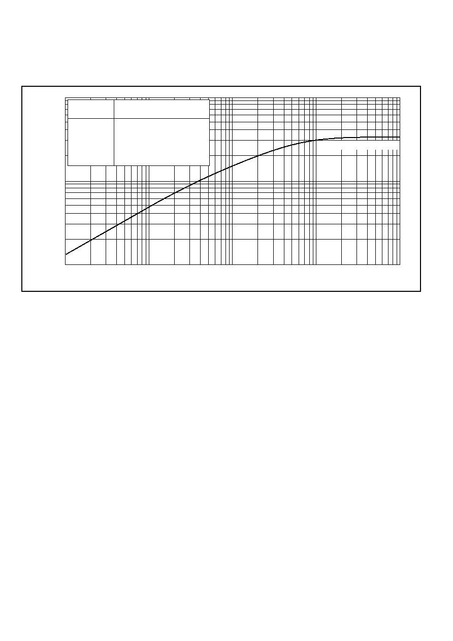
CURVES
Fig.2 Maximum (limit) on-state characteristics
ORDERING INFORMATION
PT
Pulse Power Thyristor
40Q Device type
P
Package outline type code
x
lead length (see table, right)
45
Voltage x100
Lead length (x)
O
C
D
E
F
G
H
J
K
L
No lead
8"
10"
12"
16"
18"
20"
24"
30"
40"
200mm
250mm
300mm
400mm
450mm
500mm
600mm
750mm
1000mm
Measured under pulse conditions
1.0
2.0
3.0
4.0
5.0
Instantaneous on-state voltage V
T
- (V)
0
1000
2000
3000
4000
Instantaneous on-state current I
T
- (A)
1
2
1: T
j
= 25°C Max
2: T
j
= 125°C Max

www.dynexsemi.com
POWER ASSEMBLY CAPABILITY
The Power Assembly group was set up to provide a support service for those customers requiring more than the basic
semiconductor, and has developed a flexible range of heatsink and clamping systems in line with advances in device voltages
and current capability of our semiconductors.
We offer an extensive range of air and liquid cooled assemblies covering the full range of circuit designs in general use today.
The Assembly group offers high quality engineering support dedicated to designing new units to satisfy the growing needs of
our customers.
Using the latest CAD methods our team of design and applications engineers aim to provide the Power Assembly Complete
Solution (PACs).
HEATSINKS
The Power Assembly group has its own proprietary range of extruded aluminium heatsinks which have been designed to
optimise the performance of Dynex semiconductors. Data with respect to air natural, forced air and liquid cooling (with flow
rates) is available on request.
For further information on device clamps, heatsinks and assemblies, please contact your nearest sales representative or
Customer Services.
CUSTOMER SERVICE
Tel: +44 (0)1522 502753 / 502901. Fax: +44 (0)1522 500020
SALES OFFICES
Benelux, Italy & Switzerland: Tel: +33 (0)1 64 66 42 17. Fax: +33 (0)1 64 66 42 19.
France: Tel: +33 (0)2 47 55 75 52. Fax: +33 (0)2 47 55 75 59.
Germany, Northern Europe, Spain & Rest Of World: Tel: +44 (0)1522 502753 / 502901.
Fax: +44 (0)1522 500020
North America: Tel: (613) 723-7035. Fax: (613) 723-1518. Toll Free: 1.888.33.DYNEX (39639) /
Tel: (949) 733-3005. Fax: (949) 733-2986.
These offices are supported by Representatives and Distributors in many countries world-wide.
© Dynex Semiconductor 2002 TECHNICAL DOCUMENTATION NOT FOR RESALE. PRODUCED IN
UNITED KINGDOM
HEADQUARTERS OPERATIONS
DYNEX SEMICONDUCTOR LTD
Doddington Road, Lincoln.
Lincolnshire. LN6 3LF. United Kingdom.
Tel: +44-(0)1522-500500
Fax: +44-(0)1522-500550
This publication is issued to provide information only which (unless agreed by the Company in writing) may not be used, applied or reproduced for any purpose nor form part of any order or contract nor to be regarded
as a representation relating to the products or services concerned. No warranty or guarantee express or implied is made regarding the capability, performance or suitability of any product or service. The Company
reserves the right to alter without prior notice the specification, design or price of any product or service. Information concerning possible methods of use is provided as a guide only and does not constitute any guarantee
that such methods of use will be satisfactory in a specific piece of equipment. It is the user's responsibility to fully determine the performance and suitability of any equipment using such information and to ensure
that any publication or data used is up to date and has not been superseded. These products are not suitable for use in any medical products whose failure to perform may result in significant injury
or death to the user. All products and materials are sold and services provided subject to the Company's conditions of sale, which are available on request.
All brand names and product names used in this publication are trademarks, registered trademarks or trade names of their respective owners.
http://www.dynexsemi.com
e-mail: power_solutions@dynexsemi.com
Datasheet Annotations:
Dynex Semiconductor annotate datasheets in the top right hard corner of the front page, to indicate product status. The annotations are as follows:-
Target Information: This is the most tentative form of information and represents a very preliminary specification. No actual design work on the product has been started.
Preliminary Information: The product is in design and development. The datasheet represents the product as it is understood but details may change.
Advance Information: The product design is complete and final characterisation for volume production is well in hand.
No Annotation: The product parameters are fixed and the product is available to datasheet specification.