Publication# 14128
Rev. I
Amendment /0
Issue Date: May 1995
MACH210A-7/10/12
MACH210-12/15/20
MACH210AQ-12/15/20
High-Density EE CMOS Programmable Logic
FINAL
COM'L: -7/10/12/15/20, Q-12/15/20 IND: -12/14/18/24
DISTINCTIVE CHARACTERISTICS
44 Pins
64 Macrocells
7.5 ns t
PD
Commercial
12 ns t
PD
Industrial
133 MHz f
CNT
38 Inputs; 210A Inputs have built-in pull-up
resistors
Peripheral Component Interconnect (PCI)
compliant
32 Outputs
64 Flip-flops; 2 clock choices
4 "PAL22V16" blocks with buried macrocells
Pin-compatible with MACH110, MACH111,
MACH211, and MACH215
GENERAL DESCRIPTION
The MACH210 is a member of the high-performance
EE CMOS MACH 2
device family. This device has
approximately six times the logic macrocell capability of
the popular PAL22V10 without loss of speed.
The MACH210 consists of four PAL blocks intercon-
nected by a programmable switch matrix. The four PAL
blocks are essentially "PAL22V16" structures complete
with product-term arrays and programmable macro-
cells, including additional buried macrocells. The switch
matrix connects the PAL blocks to each other and to all
input pins, providing a high degree of connectivity
between the fully-connected PAL blocks. This allows
designs to be placed and routed efficiently.
The MACH210 has two kinds of macrocell: output and
buried. The MACH210 output macrocell provides regis-
tered, latched, or combinatorial outputs with program-
mable polarity. If a registered configuration is chosen,
the register can be configured as D-type or T-type to
help reduce the number of product terms. The register
type decision can be made by the designer or by the
software. All output macrocells can be connected to an
I/O cell. If a buried macrocell is desired, the internal
feedback path from the macrocell can be used, which
frees up the I/O pin for use as an input.
The MACH210 has dedicated buried macrocells which,
in addition to the capabilities of the output macrocell,
also provide input registers or latches for use in
synchronizing signals and reducing setup time require-
ments.
Lattice Semiconductor

3
MACH210-7/10/12/15/20, Q-12/15/20
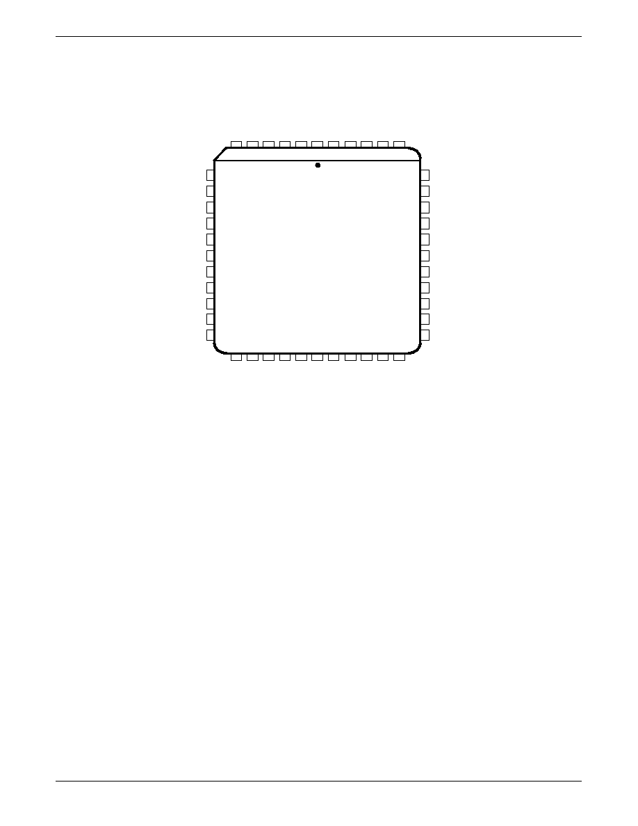
CONNECTION DIAGRAM
Top View
PLCC
14128I-2
I/O5
I/O6
I/O7
I0
I1
CLK0/I2
I/O8
I/O9
GND
I/O10
I/O11
I/O
4
I/O
3
I/O
2
I/O
1
I/O
0
GND
V
CC
I/O
31
I/O
30
I/O
29
I/O
28
I/O27
I/O26
I/O25
I3
I4
I/O24
CLK1/I5
GND
I/O23
I/O22
I/O21
I/O
12
I/O
13
I/O
14
V
CC
GND
I/O
16
I/O
15
I/O
17
I/O
18
I/O
19
I/O
20
7
8
9
10
11
12
13
15
16
14
17
5
6
1
3
2
4
44 43 42 41 40
29
30
31
32
33
34
35
36
37
38
39
18
28
27
26
25
24
23
22
21
19 20
Note:
Pin-compatible with MACH110, MACH111, MACH211, and MACH215.

MACH210-7/10/12/15/20, Q-12/15/20
4
CONNECTION DIAGRAM
Top View
TQFP
1
2
3
4
5
6
7
8
9
10
11
I/O27
I/O26
I/O25
I/O24
CLK1/I5
GND
I4
I3
I/O23
I/O22
I/O21
33
32
31
30
29
28
27
26
25
24
23
I/O5
I/O6
I/O7
I0
I1
GND
CLK0/I2
I/O8
I/O9
I/O10
I/O11
44
43
42
41
40
39
38
37
36
35
34
I/O4
I/O3
I/O2
I/O1
I/O0
GND
V
CC
I/O31
I/O30
I/O29
I/O28
12
13
14
15
16
17
18
19
20
21
22
I/O12
I/O13
I/O14
I/O15
V
CC
GND
I/O16
I/O17
I/O18
I/O19
I/O20
14128I-3
Note:
Pin-compatible with MACH111 and MACH211.
PIN DESIGNATIONS
CLK/I =
Clock or Input
GND
=
Ground
I
=
Input
I/O
=
Input/Output
V
CC
=
Supply Voltage

MACH210-7/10/12/15/20, Q-12/15/20 (Com'l)
5
ORDERING INFORMATION
Commercial Products
Programmable logic products for commercial applications are available with several ordering options. The order number
(Valid Combination) is formed by a combination of:
OPERATING CONDITIONS
C = Commercial (0
�
C to +70
�
C)
FAMILY TYPE
MACH = Macro Array CMOS High-Speed
SPEED
-7
= 7.5 ns t
PD
-10 = 10 ns t
PD
-12 = 12 ns t
PD
-15 = 15 ns t
PD
-20 = 20 ns t
PD
MACH210A-7
MACH210A-10
MACH210A-12
MACH210-12
MACH210-15
MACH210-20
MACH210AQ-12
MACH210AQ-15
MACH210AQ-20
MACH
-7
J
C
Valid Combinations
The Valid Combinations table lists configurations
planned to be supported in volume for this device. Con-
sult your local sales office to confirm availability of
specific valid combinations or to check on newly re-
leased combinations.
Valid Combinations
OPTIONAL PROCESSING
Blank = Standard Processing
210A
DEVICE NUMBER
210
= 64 Macrocells, 44 Pins
210A
= 64 Macrocells, 44 Pins, Input Pull-Up Resistors
210AQ = 64 Macrocells, 44 Pins, Input Pull-Up Resistors,
Quarter Power
PACKAGE TYPE
J = 44-Pin Plastic Leaded Chip
Carrier (PL 044)
V = 44-Pin Thin Quad Flat Pack
(PQT044)
JC
JC,
VC


