
1
GAL16V8/883
High Performance E
2
CMOS PLD
Generic Array LogicTM
Features
· HIGH PERFORMANCE E
2
CMOS
®
TECHNOLOGY
-- 7.5 ns Maximum Propagation Delay
-- Fmax = 100 MHz
-- 6 ns Maximum from Clock Input to Data Output
-- TTL Compatible 12 mA Outputs
-- UltraMOS
®
Advanced CMOS Technology
· 50% REDUCTION IN POWER FROM BIPOLAR
-- 75mA Typ Icc
· ACTIVE PULL-UPS ON ALL PINS (GAL16V8D-7 and
GAL16V8D-10)
· E
2
CELL TECHNOLOGY
-- Reconfigurable Logic
-- Reprogrammable Cells
-- 100% Tested/100% Yields
-- High Speed Electrical Erasure (<100ms)
-- 20 Year Data Retention
· EIGHT OUTPUT LOGIC MACROCELLS
-- Maximum Flexibility for Complex Logic Designs
-- Programmable Output Polarity
-- Also Emulates 20-pin PAL
®
Devices with Full Function/
Fuse Map/Parametric Compatibility
· PRELOAD AND POWER-ON RESET OF ALL REGISTERS
-- 100% Functional Testability
· APPLICATIONS INCLUDE:
-- DMA Control
-- State Machine Control
-- High Speed Graphics Processing
-- Standard Logic Speed Upgrade
· ELECTRONIC SIGNATURE FOR IDENTIFICATION
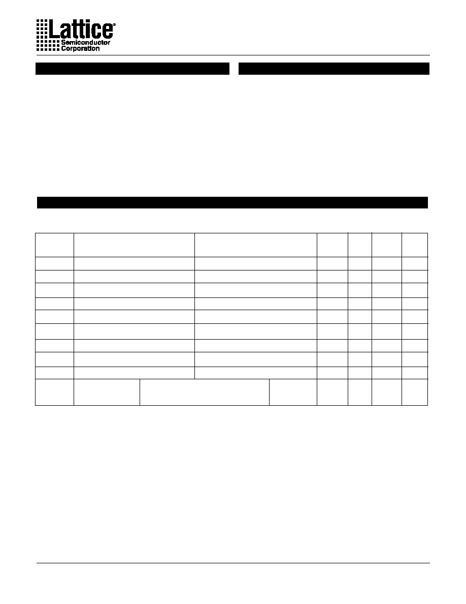
I/CLK
I
I/O/Q
I
I/O/Q
I
I/O/Q
I
I/O/Q
I
I/O/Q
I
I/O/Q
I
I/O/Q
I
I/O/Q
CLK
8
8
8
8
8
8
8
8
OE
OLMC
OLMC
OLMC
OLMC
OLMC
OLMC
OLMC
OLMC
PROGRAMMABLE
AND-ARRAY
(64 X 32)
I/OE
Description
The GAL16V8/883 is a high performance E
2
CMOS program-
mable logic device processed in full compliance to MIL-STD-883.
This military grade device combines a high performance CMOS
process with Electrically Erasable (E
2
) floating gate technology to
provide the highest speed/power performance available in the
883 qualified PLD market. The GAL16V8D/883, at 7.5ns maxi-
mum propagation delay time, is the world's fastest military quali-
fied CMOS PLD.
The generic GAL architecture provides maximum design flexibil-
ity by allowing the Output Logic Macrocell (OLMC) to be config-
ured by the user. The GAL16V8/883 is capable of emulating all
standard 20-pin PAL
®
devices with full function/fuse map/para-
metric compatibility.
Unique test circuitry and reprogrammable cells allow complete
AC, DC, and functional testing during manufacture. Therefore,
Lattice Semiconductor delivers 100% field programmability and
functionality of all GAL products. In addition, 100 erase/write
cycles and data retention in excess of 20 years are specified.
2
20
I/CLK
I
I
I
I
I
I
I
I
GND
Vcc
I/O/Q
I/O/Q
I/O/Q
I/O/Q
I/O/Q
I/O/Q
I/O/Q
I/O/Q
I/OE
3
4
6
8
9
11
13
14
16
18
19
1
10
11
20
I/CLK
I
I
I
I
I
I
I
I
GND
Vcc
I/O/Q
I/O/Q
I/O/Q
I/O/Q
I/O/Q
I/O/Q
I/O/Q
I/O/Q
I/OE
5
15
GAL16V8
Top View
LCC
CERDIP
GAL
16V8
Copyright © 1999 Lattice Semiconductor Corp. All brand or product names are trademarks or registered trademarks of their respective holders. The specifications and information herein are subject
to change without notice.
LATTICE SEMICONDUCTOR CORP., 5555 Northeast Moore Ct., Hillsboro, Oregon 97124, U.S.A.
February 1999
Tel. (503) 268-8000; 1-800-LATTICE; FAX (503) 268-8556; http://www.latticesemi.com
16v8mil_03
Functional Block Diagram
Pin Configuration
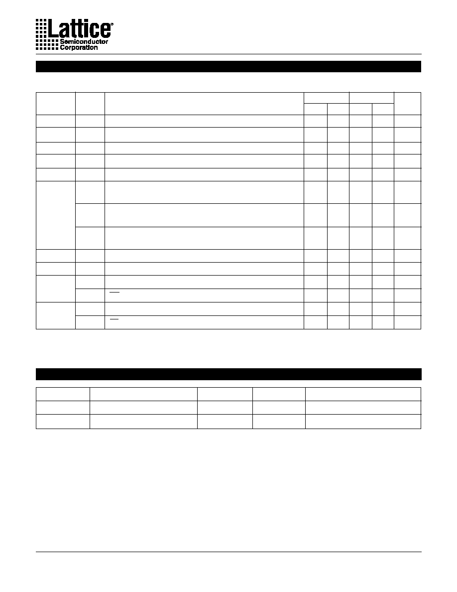
Specifications
GAL16V8D-7/10/883
2
V
IL
Input Low Voltage
Vss 0.5
--
0.8
V
V
IH
Input High Voltage
2.0
--
Vcc+1
V
I
IL
1
Input or I/O Low Leakage Current
0V
V
IN
V
IL
(MAX.)
--
--
100
µ
A
I
IH
Input or I/O High Leakage Current
3.5V
V
IN
V
CC
--
--
10
µ
A
V
OL
Output Low Voltage
I
OL
= MAX. Vin = V
IL
or V
IH
--
--
0.5
V
V
OH
Output High Voltage
I
OH
= MAX. Vin = V
IL
or V
IH
2.4
--
--
V
I
OL
Low Level Output Current
--
--
12
mA
I
OH
High Level Output Current
--
--
2
mA
I
OS
2
Output Short Circuit Current
V
CC
= 5V
V
OUT
= 0.5V T
A
= 25
°
C
30
--
150
mA
I
CC
Operating Power
V
IL
= 0.5V V
IH
= 3.0V
L-7/-10
--
75
130
mA
Supply Current
f
toggle
= 15MHz Outputs Open
1) The leakage current is due to the internal pull-up on all pins. See Input Buffer section for more information.
2) One output at a time for a maximum duration of one second. Vout = 0.5V was selected to avoid test problems caused by tester
ground degradation. Characterized but not 100% tested.
3) Typical values are at Vcc = 5V and T
A
= 25
°
C
Recommended Operating Conditions
Case Temperature (T
C
) .............................. 55 to 125
°
C
Supply voltage (V
CC
)
with Respect to Ground ..................... +4.50 to +5.50V
DC Electrical Characteristics
Over Recommended Operating Conditions (Unless Otherwise Specified)
SYMBOL
PARAMETER
CONDITION
MIN.
TYP.
3
MAX.
UNITS
Absolute Maximum Ratings
(1)
Supply voltage V
CC
...................................... 0.5 to +7V
Input voltage applied .......................... 2.5 to V
CC
+1.0V
Off-state output voltage applied ......... 2.5 to V
CC
+1.0V
Storage Temperature ................................ 65 to 150
°
C
Case Temperature with
Power Applied ........................................ 55 to 125
°
C
1.Stresses above those listed under the "Absolute Maximum Rat-
ings" may cause permanent damage to the device. These are
stress only ratings and functional operation of the device at these
or at any other conditions above those indicated in the operational
sections of this specification is not implied (while programming,
follow the programming specifications).
Specifications
GAL16V8D-7/10/883
3
t
pd
A
Input or I/O to Combinational Output
1
7.5
2
10
ns
t
co
A
Clock to Output Delay
1
6
1
7
ns
t
cf
2
--
Clock to Feedback Delay
--
6
--
7
ns
t
su
--
Setup Time, Input or Feedback before Clock
7
--
10
--
ns
t
h
--
Hold Time, Input or Feedback after Clock
0
--
0
--
ns
A
Maximum Clock Frequency with
76.9
--
58.8
--
MHz
External Feedback, 1/(tsu + tco)
f
max
3
A
Maximum Clock Frequency with
76.9
--
58.8
--
MHz
Internal Feedback, 1/(tsu + tcf)
A
Maximum Clock Frequency with
100
--
62.5
--
MHz
No Feedback
t
wh
--
Clock Pulse Duration, High
5
--
8
--
ns
t
wl
--
Clock Pulse Duration, Low
5
--
8
--
ns
t
en
B
Input or I/O to Output Enabled
1
9
--
10
ns
B
OE to Output Enabled
1
7
--
10
ns
t
dis
C
Input or I/O to Output Disabled
1
9
--
10
ns
C
OE to Output Disabled
1
7
--
10
ns
PARAMETER
UNITS
TEST
COND
1
.
DESCRIPTION
1) Refer to Switching Test Conditions section.
2) Calculated from fmax with internal feedback. Refer to fmax Descriptions section.
3) Refer to fmax Descriptions section.
SYMBOL
PARAMETER
MAXIMUM*
UNITS
TEST CONDITIONS
C
I
Input Capacitance
10
pF
V
CC
= 5.0V, V
I
= 2.0V
C
I/O
I/O Capacitance
10
pF
V
CC
= 5.0V, V
I/O
= 2.0V
*Characterized but not 100% tested.
-10
MIN. MAX.
-7
MIN. MAX.
Capacitance (T
A
= 25
°
C, f = 1.0 MHz)
AC Switching Characteristics
Over Recommended Operating Conditions

Specifications
GAL16V8D/883
4
V
IL
Input Low Voltage
Vss 0.5
--
0.8
V
V
IH
Input High Voltage
2.0
--
Vcc+1
V
I
IL
Input or I/O Low Leakage Current
0V
V
IN
V
IL
(MAX.)
--
--
10
µ
A
I
IH
Input or I/O High Leakage Current
3.5V
V
IN
V
CC
--
--
10
µ
A
V
OL
Output Low Voltage
I
OL
= MAX. Vin = V
IL
or V
IH
--
--
0.5
V
V
OH
Output High Voltage
I
OH
= MAX. Vin = V
IL
or V
IH
2.4
--
--
V
I
OL
Low Level Output Current
--
--
12
mA
I
OH
High Level Output Current
--
--
2
mA
I
OS
1
Output Short Circuit Current
V
CC
= 5V
V
OUT
= 0.5V T
A
= 25
°
C
30
--
150
mA
I
CC
Operating Power
V
IL
= 0.5V V
IH
= 3.0V
L -15/ -20/-30
--
75
130
mA
Supply Current
f
toggle
= 15MHz Outputs Open
1) One output at a time for a maximum duration of one second. Vout = 0.5V was selected to avoid test problems caused by tester
ground degradation. Characterized but not 100% tested.
3) Typical values are at Vcc = 5V and T
A
= 25
°
C
DC Electrical Characteristics
Over Recommended Operating Conditions (Unless Otherwise Specified)
SYMBOL
PARAMETER
CONDITION
MIN.
TYP.
2
MAX.
UNITS
Absolute Maximum Ratings
(1)
Supply voltage V
CC
...................................... 0.5 to +7V
Input voltage applied .......................... 2.5 to V
CC
+1.0V
Off-state output voltage applied ......... 2.5 to V
CC
+1.0V
Storage Temperature ................................ 65 to 150
°
C
Case Temperature with
Power Applied ........................................ 55 to 125
°
C
1.Stresses above those listed under the "Absolute Maximum Rat-
ings" may cause permanent damage to the device. These are
stress only ratings and functional operation of the device at these
or at any other conditions above those indicated in the operational
sections of this specification is not implied (while programming,
follow the programming specifications).
Recommended Operating Conditions
Case Temperature (T
C
) .............................. 55 to 125
°
C
Supply voltage (V
CC
)
with Respect to Ground ..................... +4.50 to +5.50V

Specifications
GAL16V8D/883
5
Capacitance (T
A
= 25
°
C, f = 1.0 MHz)
SYMBOL
PARAMETER
MAXIMUM*
UNITS
TEST CONDITIONS
C
I
Input Capacitance
10
pF
V
CC
= 5.0V, V
I
= 2.0V
C
I/O
I/O Capacitance
10
pF
V
CC
= 5.0V, V
I/O
= 2.0V
*Characterized but not 100% tested.
t
pd
A
Input or I/O to Combinational Output
3
15
3
20
3
30
ns
t
co
A
Clock to Output Delay
2
12
2
15
2
20
ns
t
cf
2
--
Clock to Feedback Delay
--
12
--
15
--
20
ns
t
su
--
Setup Time, Input or Feedback before Clock
12
--
15
--
25
--
ns
t
h
--
Hold Time, Input or Feedback after Clock
0
--
0
--
0
--
ns
A
Maximum Clock Frequency with
41.6
--
33.3
--
22.2
--
MHz
External Feedback, 1/(tsu + tco)
f
max
3
A
Maximum Clock Frequency with
41.6
--
33.3
--
22.2
--
MHz
Internal Feedback, 1/(tsu + tcf)
A
Maximum Clock Frequency with
50
--
41.6
--
33.3
--
MHz
No Feedback
t
wh
--
Clock Pulse Duration, High
10
--
12
--
15
--
ns
t
wl
--
Clock Pulse Duration, Low
10
--
12
--
15
--
ns
t
en
B
Input or I/O to Output Enabled
--
15
--
20
--
30
ns
B
OE to Output Enabled
--
15
--
18
--
25
ns
t
dis
C
Input or I/O to Output Disabled
--
15
--
20
--
30
ns
C
OE to Output Disabled
--
15
--
18
--
25
ns
1) Refer to Switching Test Conditions section.
2) Calculated from fmax with internal feedback. Refer to fmax Descriptions section.
3) Refer to fmax Descriptions section.
-20
MIN. MAX.
-15
MIN. MAX.
PARAMETER
UNITS
DESCRIPTION
TEST
COND
1
.
-30
MIN. MAX.
AC Switching Characteristics
Over Recommended Operating Conditions