1 - 2
© 2001 IXYS All rights reserved
IXYS Semiconductor GmbH
Edisonstr. 15,
D-68623 Lampertheim
Phone: +49-6206-503-0, Fax: +49-6206-503627
IXYS Corporation
3540 Bassett Street, Santa Clara CA 95054
Phone: (408) 982-0700, Fax: 408-496-0670
Advanced Technical Information
106
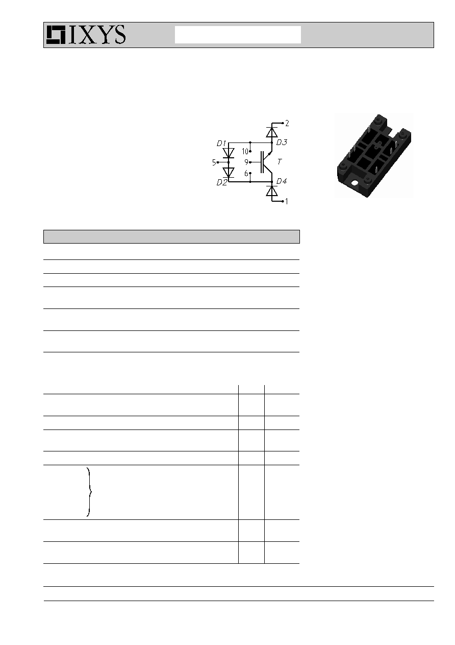
Rectifier Module for
Three Phase Power Factor Correction
IXYS reserves the right to change limits, test conditions and dimensions.
VUI 30-12 N1
Typical Rectified Mains Power
P
n
= 15 kW
at V
n
= 400 V 3~; f
T
= 15 kHz; T
C
= 80°C
Features
· NPT IGBT with low saturation voltage
· fast recovery epitaxial diodes (FRED)
· module package:
- high level of integration
- solder terminals for PCB mounting
- isolated DCB ceramic base plate
- large creepage and strike distances
Applications
Three phase rectifier with power factor
correction, set up as follows:
· input from three phase mains
- wide range of input voltage
- mains currents approximately sinusoidal
in phase with mains voltage
- topology permits to control overcurrent
such as in case of input voltage peaks
· output
- direct current link
- buck type converter - reduced output
voltage
- possibility to supply boost converter,
inverter etc.
· required components
- one power semiconductor module per
phase
- one inductor and one capacitor per
phase on mains side
- output inductor, depending on supplied
circuit
Transistor T
Symbol
Conditions
Maximum Ratings
V
CES
T
VJ
= 25°C to 150°C
1200
V
V
GES
±
20
V
I
C25
T
C
= 25°C
95
A
I
C80
T
C
= 80°C
65
A
I
CM
V
GE
=
±
15 V; R
G
= 22
; T
VJ
= 125°C
100
A
V
CEK
RBSOA; L = 100 µH
V
CES
t
SC
V
CE
= V
CES
; V
GE
=
±
15 V; R
G
= 22
; T
VJ
= 125°C
10
µs
(SCSOA)
non-repetitive
Symbol
Conditions
Characteristic Values
(T
VJ
= 25
°
C, unless otherwise specified)
min.
typ.
max.
V
CE(sat)
I
C
= 20 A; V
GE
= 15 V; T
VJ
= 25°C
1.7
2.0
V
T
VJ
= 125°C
1.9
V
V
GE(th)
I
C
= 2 mA; V
GE
= V
CE
4.5
6.5
V
I
CES
V
CE
= V
CES
;
V
GE
= 0 V; T
VJ
= 25°C
1.6
mA
T
VJ
= 125°C
1.8
mA
I
GES
V
CE
= 0 V; V
GE
=
±
20 V
400
nA
t
d(on)
100
ns
t
r
70
ns
t
d(off)
500
ns
t
f
70
ns
E
on
3.0
mJ
E
off
2.2
mJ
C
ies
V
CE
= 25 V; V
GE
= 0 V; f = 1 MHz
3.3
nF
Q
Gon
V
CE
= 600 V; V
GE
= 15 V; I
C
= 50 A
240
nC
R
thJC
0.3 K/W
R
thJH
with heatsink transfer paste
0.6
K/W
Inductive load, T
VJ
= 125°C
V
CE
= 600 V; I
C
= 20 A
V
GE
= ±15 V; R
G
= 22

2 - 2
© 2001 IXYS All rights reserved
IXYS Semiconductor GmbH
Edisonstr. 15,
D-68623 Lampertheim
Phone: +49-6206-503-0, Fax: +49-6206-503627
IXYS Corporation
3540 Bassett Street, Santa Clara CA 95054
Phone: (408) 982-0700, Fax: 408-496-0670
Advanced Technical Information
106
Module
Symbol
Conditions
Maximum Ratings
T
VJ
-40...+150
°
C
T
stg
-40...+125
°
C
V
ISOL
I
ISOL
1 mA; 50/60 Hz; t = 1 min
3600
V~
M
d
Mounting torque (M5)
2 - 2.5
Nm
Symbol
Conditions
Characteristic Values
(T
VJ
= 25
°
C, unless otherwise specified)
min.
typ.
max.
d
A
, d
S
5
mm
Weight
35
g
Diodes D1 - D4
Symbol
Conditions
Maximum Ratings
V
RRM
T
VJ
= 25°C to 150°C
1200
V
I
F25
T
C
= 25°C
40
A
I
F80
T
C
= 80°C
25
A
Symbol
Conditions
Characteristic Values
min.
typ.
max.
V
F
I
F
= 20 A; T
VJ
= 25°C
2.2
2.4
V
T
VJ
= 125°C
1.9
V
I
R
V
R
= V
RRM
;
T
VJ
= 25°C
0.75
mA
V
R
= 0.8V
RRM
; T
VJ
= 125°C
2
mA
I
RM
I
F
= 30A; di
F
/dt = -250 A/µs; T
VJ
= 125°C
16
A
t
rr
V
R
= 540 V
400
ns
R
thJC
1.3 K/W
R
thJH
with heat transfer paste
2.6
K/W
Dimensions in mm (1 mm = 0.0394")
VUI 30-12 N1