© 2001 IXYS All rights reserved
1 - 8
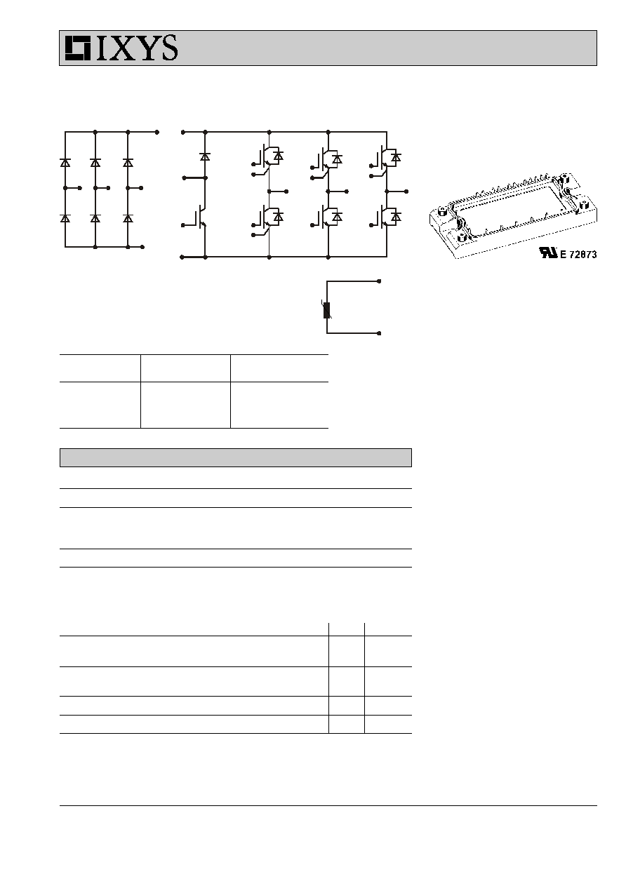
Converter - Brake - Inverter Module
(CBI2)
Input Rectifier Bridge D11 - D16
Symbol
Conditions
Maximum Ratings
V
RRM
1600
V
I
FAV
T
C
= 80°C; sine 180°
30
A
I
DAVM
T
C
= 80°C; rectangular; d = 1/3
29
A
I
FSM
T
VJ
= 25°C; t = 10 ms; sine 50 Hz
400
A
P
tot
T
C
= 25°C
120
W
Symbol
Conditions
Characteristic Values
(T
VJ
= 25
°
C, unless otherwise specified)
min.
typ.
max.
V
F
I
F
= 50 A; T
VJ
= 25°C
1.5
1.8
V
T
VJ
= 125°C
1.6
V
I
R
V
R
= V
RRM
;
T
VJ
= 25°C
0.2
mA
T
VJ
= 125°C
2
mA
t
rr
V
R
= 100 V;
I
F
= 20 A; di/dt = -20 A/µs
1
µs
R
thJC
(per diode)
1.06 K/W
Three Phase
Brake Chopper
Three Phase
Rectifier
Inverter
V
RRM
= 1600V
V
CES
= 600 V
V
CES
= 600 V
I
DAVM
= 44 A
I
C25
= 35 A
I
C25
= 75 A
I
FSM
= 400 A
V
CE(sat)
= 2.1 V
V
CE(sat)
= 1.9 V
10
5
MUBW 50-06 A7
IXYS reserves the right to change limits, test conditions and dimensions.
NTC
D11
D13
D15
D12
D14
D16
1
2
3
D7
T7
T1
D1
T3
D3
T2
T4
T6
T5
D4
D2
D6
D5
21
22
7
6
4
5
16
15
18
17
20
19
11
10
23
24
14
8
9
12
13
Application: AC motor drives with
q
Input from single or three phase grid
q
Three phase synchronous or
asynchronous motor
q
electric braking operation
Features
q
High level of integration - only one power
semiconductor module required for the
whole drive
q
Fast rectifier diodes for enhanced EMC
behaviour
q
NPT IGBT technology with low
saturation voltage, low switching
losses, high RBSOA and short circuit
ruggedness
q
Epitaxial free wheeling diodes with
Hiperfast and soft reverse recovery
q
Industry standard package with insulated
copper base plate and soldering pins for
PCB mounting
q
Temperature sense included

© 2001 IXYS All rights reserved
2 - 8
MUBW 50-06 A7
Equivalent Circuits for Simulation
Conduction
D11 - D16
Rectifier Diode (typ. at T
J
= 125°C)
V
0
= 1.0 V; R
0
= 12 m
T1 - T6 / D1 - D6
IGBT (typ. at V
GE
= 15 V; T
J
= 125°C)
V
0
= 0.82 V; R
0
= 28 m
Free Wheeling Diode (typ. at T
J
= 125°C)
V
0
= 0.89 V; R
0
= 8 m
T7 / D7
IGBT (typ. at V
GE
= 15 V; T
J
= 125°C)
V
0
= 0.9 V; R
0
= 65 m
Free Wheeling Diode (typ. at T
J
= 125°C)
V
0
= 1.07 V; R
0
= 23 m
Thermal Response
D11 - D16
Rectifier Diode (typ.)
C
th1
= 0.131 J/K; R
th1
= 0.851 K/W
C
th2
= 0.839 J/K; R
th2
= 0.209 K/W
T1 - T6 / D1 - D6
IGBT (typ.)
C
th1
= 0.221 J/K; R
th1
= 0.382 K/W
C
th2
= 1.377 J/K; R
th2
= 0.119 K/W
Free Wheeling Diode (typ.)
C
th1
= 0.116 J/K; R
th1
= 0.973 K/W
C
th2
= 0.88 J/K; R
th2
= 0.217 K/W
T7 / D7
IGBT (typ.)
C
th1
= 0.108 J/K; R
th1
= 0.79 K/W
C
th2
= 0.921 J/K; R
th2
= 0.209 K/W
Free Wheeling Diode (typ.)
C
th1
= 0.043 J/K; R
th1
= 2.738 K/W
C
th2
= 0.54 J/K; R
th2
= 0.462 K/W
Output Inverter T1 - T6
Symbol
Conditions
Maximum Ratings
V
CES
T
VJ
= 25°C to 150°C
600
V
V
GES
Continuous
±
20
V
V
GEM
Transient
±
30
V
I
C25
T
C
= 25°C
75
A
I
C80
T
C
= 80°C
50
A
RBSOA
V
GE
=
±
15 V; R
G
= 22
; T
VJ
= 125°C
I
CM
= 100
A
Clamped inductive load; L = 100 µH
V
CEK
V
CES
t
SC
V
CE
= V
CES
; V
GE
=
±
15 V; R
G
= 22
; T
VJ
= 125°C
10
µs
(SCSOA)
non-repetitive
P
tot
T
C
= 25°C
250
W
Symbol
Conditions
Characteristic Values
(T
VJ
= 25
°
C, unless otherwise specified)
min.
typ.
max.
V
CE(sat)
I
C
= 50 A; V
GE
= 15 V; T
VJ
= 25°C
1.9
2.4
V
T
VJ
= 125°C
2.2
V
V
GE(th)
I
C
= 1 mA; V
GE
= V
CE
4.5
6.5
V
I
CES
V
CE
= V
CES
;
V
GE
= 0 V; T
VJ
= 25°C
0.8
mA
T
VJ
= 125°C
0.7
mA
I
GES
V
CE
= 0 V; V
GE
=
±
20 V
200
nA
t
d(on)
50
ns
t
r
55
ns
t
d(off)
300
ns
t
f
30
ns
E
on
2.3
mJ
E
off
1.7
mJ
C
ies
V
CE
= 25 V; V
GE
= 0 V; f = 1 MHz
2800
pF
Q
Gon
V
CE
= 300V; V
GE
= 15 V; I
C
= 50 A
120
nC
R
thJC
(per IGBT)
0.5 K/W
Inductive load, T
VJ
= 125°C
V
CE
= 300 V; I
C
= 50 A
V
GE
= ±15 V; R
G
= 22
Output Inverter D1 - D6
Symbol
Conditions
Maximum Ratings
I
F25
T
C
= 25°C
72
A
I
F80
T
C
= 80°C
45
A
Symbol
Conditions
Characteristic Values
min.
typ.
max.
V
F
I
F
= 50 A; V
GE
= 0 V; T
VJ
= 25°C
1.8
V
T
VJ
= 125°C
1.3
V
I
RM
I
F
= 25 A; di
F
/dt = -500 A/µs; T
VJ
= 125°C
25
A
t
rr
V
R
= 300 V; V
GE
= 0 V
90
ns
R
thJC
(per diode)
1.19 K/W

© 2001 IXYS All rights reserved
3 - 8
MUBW 50-06 A7
Brake Chopper T7
Symbol
Conditions
Maximum Ratings
V
CES
T
VJ
= 25°C to 150°C
600
V
V
GES
Continuous
±
20
V
V
GEM
Transient
±
30
V
I
C25
T
C
= 25°C
35
A
I
C80
T
C
= 80°C
25
A
RBSOA
V
GE
=
±
15 V; R
G
= 47
; T
VJ
= 125°C
I
CM
= 40
A
Clamped inductive load; L = 100 µH
V
CEK
V
CES
t
SC
V
CE
= V
CES
; V
GE
=
±
15 V; R
G
= 47
; T
VJ
= 125°C
10
µs
(SCSOA)
non-repetitive
P
tot
T
C
= 25°C
125
W
Symbol
Conditions
Characteristic Values
(T
VJ
= 25
°
C, unless otherwise specified)
min.
typ.
max.
V
CE(sat)
I
C
= 25 A; V
GE
= 15 V; T
VJ
= 25°C
2.1
2.6
V
T
VJ
= 125°C
2.4
V
V
GE(th)
I
C
= 0.5 mA; V
GE
= V
CE
4.5
6.5
V
I
CES
V
CE
= V
CES
;
V
GE
= 0 V; T
VJ
= 25°C
0.5
mA
T
VJ
= 125°C
0.3
mA
I
GES
V
CE
= 0 V; V
GE
=
±
20 V
200
nA
t
d(on)
50
ns
t
r
60
ns
t
d(off)
300
ns
t
f
30
ns
E
on
1.15
mJ
E
off
0.85
mJ
C
ies
V
CE
= 25 V; V
GE
= 0 V; f = 1 MH z
1100
pF
Q
Gon
V
CE
= 300 V; V
GE
= 15 V; I
C
= 25 A
65
nC
R
thJC
1.0 K/W
Brake Chopper D7
Symbol
Conditions
Maximum Ratings
V
RRM
T
VJ
= 25°C to 150°C
600
V
I
F25
T
C
= 25°C
22
A
I
F80
T
C
= 80°C
15
A
Symbol
Conditions
Characteristic Values
min.
typ.
max.
V
F
I
F
= 25 A; T
VJ
= 25°C
2.5
V
T
VJ
= 125°C
1.8
V
I
R
V
R
= V
RRM
;
T
VJ
= 25°C
0.06
mA
T
VJ
= 125°C
0.07
mA
I
RM
I
F
= 10 A; di
F
/dt = -400 A/µs; T
VJ
= 125°C
11
A
t
rr
V
R
= 300 V
80
ns
R
thJC
3.2 K/W
Inductive load, T
VJ
= 125°C
V
CE
= 300 V; I
C
= 25 A
V
GE
= ±15 V; R
G
= 47
© 2001 IXYS All rights reserved
4 - 8
MUBW 50-06 A7
Temperature Sensor NTC
Symbol
Conditions
Characteristic Values
min.
typ.
max.
R
25
T = 25°C
4.75
5.0
5.25
k
B
25/50
3375
K
Module
Symbol
Conditions
Maximum Ratings
T
VJ
Operating
-40...+125
°
C
T
JM
150
°
C
T
stg
-40...+125
°
C
V
ISOL
I
ISOL
1 mA; 50/60 Hz
2500
V~
M
d
Mounting torque (M5)
2.7 - 3.3
Nm
Symbol
Conditions
Characteristic Values
min.
typ.
max.
R
pin-chip
5
m
d
S
Creepage distance on surface
6
mm
d
A
Strike distance in air
6
mm
R
thCH
with heatsink compound
0.02
K/W
Weight
180
g
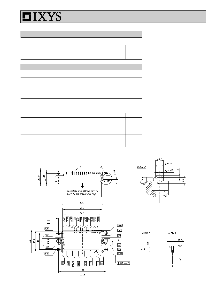
Dimensions in mm (1 mm = 0.0394")
© 2001 IXYS All rights reserved
5 - 8
MUBW 50-06 A7
0.001
0.01
0.1
1
0
40
80
120
160
200
2
3
4
5 6 7 8 9
1
10
10
2
10
3
0.0
0.5
1.0
1.5
2.0
2.5
0
20
40
60
80
100
120
0
40
80
120
0
200
400
600
800
0
20
40
60
80 100 120 140
0.001
0.01
0.1
1
10
0.0
0.2
0.4
0.6
0.8
1.0
1.2
I
2
t
I
FSM
I
F
A
V
F
t
s
t
ms
P
tot
W
I
d(AV)M
A
T
amb
t
s
K/W
A
2
s
0
20 40 60 80 100 120 140
0
20
40
60
80
100
I
d(AV)
T
C
A
V
A
°C
°C
DWFN21-16
Z
thJC
T
VJ
= 125°C
T
VJ
= 25°C
T
VJ
= 45°C
T
VJ
= 125°C
T
VJ
= 45°C
T
VJ
= 125°C
50Hz, 80% V
RRM
R
thA
:
0.05 K/W
0.15 K/W
0.3 K/W
0.5 K/W
1 K/W
2 K/W
5 K/W
Fig. 4 Power dissipation versus direct output current and ambient temperature, sin
1
8
0
°
Fig. 5 Max. forward current versus
case temperature
Fig. 6 Transient thermal impedance junction to case
Fig. 1 Forward current versus voltage
drop per diode
Fig. 2 Surge overload current
Fig. 3 I
2
t versus time per diode
Input Rectifier Bridge D11 - D16

© 2001 IXYS All rights reserved
6 - 8
MUBW 50-06 A7
0
200
400
600
800
1000
0
10
20
30
40
50
!
$
'
#
0
1
2
3
4
5
6
0
30
60
90
120
150
0
40
80
120
160
0
5
10
15
20
0
1
2
3
4
5
6
0
30
60
90
120
150
T
VJ
= 25°C
T
VJ
= 125°C
V
CE
= 300V
I
C
= 50A
V
CE
V
I
C
V
CE
A
I
C
V
nC
Q
G
-di/dt
V
V
GE
I
RM
t
rr
A/
µ
s
MUBW5006A7
T
VJ
= 125°C
V
R
= 300V
I
F
= 30A
I
RM
t
rr
9V
11V
V
GE
= 17V
15V
13V
A
9V
11V
V
GE
= 17V
15V
13V
A
4
6
8
10
12
14
16
0
30
60
90
120
150
V
CE
= 20V
V
V
GE
A
I
C
T
VJ
= 25°C
T
VJ
= 125°C
0.0
0.5
1.0
1.5
2.0
0
15
30
45
60
75
90
V
V
F
I
F
T
VJ
= 25°C
T
VJ
= 125°C
A
ns
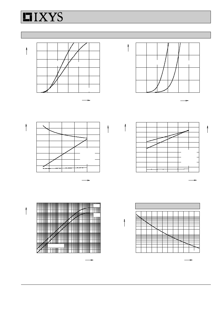
Fig. 7 Typ. output characteristics
Fig. 8 Typ. output characteristics
Fig. 9 Typ. transfer characteristics
Fig. 10 Typ. forward characteristics of
free wheeling diode
Fig. 11 Typ. turn on gate charge
Fig. 12 Typ. turn off characteristics of
free wheeling diode
Output Inverter T1 - T6 / D1 - D6

© 2001 IXYS All rights reserved
7 - 8
MUBW 50-06 A7
Fig. 13 Typ. turn on energy and switching
Fig. 14 Typ. turn off energy and switching
times versus collector current
times versus collector current
Fig. 15 Typ. turn on energy and switching
Fig.16 Typ. turn off energy and switching
times versus gate resistor
times versus gate resistor
Fig. 17 Reverse biased safe operating area
Fig. 18 Typ. transient thermal impedance
RBSOA
0
40
80
120
0.0
2.5
5.0
7.5
10.0
0
25
50
75
100
0
40
80
120
0
1
2
3
4
0
100
200
300
400
0.00001 0.0001 0.001
0.01
0.1
1
10
0.0001
0.001
0.01
0.1
1
10
0
10
20
30
40
50
60
0
1
2
3
0
200
400
600
0
10
20
30
40
50
60
0
1
2
3
4
0
20
40
60
80
single pulse
V
CE
= 300V
V
GE
= ±15V
R
G
= 22
T
VJ
= 125°C
MUBW5006A7
V
CE
= 300V
V
GE
= ±15V
I
C
= 50A
T
VJ
= 125°C
0
100
200
300
400
500
600
700
0
30
60
90
120
R
G
= 22
T
VJ
= 125°C
V
CE
= 300V
V
GE
= ±15V
R
G
= 22
T
VJ
= 125°C
E
on
V
CE
= 300V
V
GE
= ±15V
I
C
= 50A
T
VJ
= 125°C
J
d(on)
J
r
E
off
J
d(off)
J
f
E
on
J
d(on)
J
r
E
off
J
d(off)
J
f
I
C
A
I
C
A
E
off
E
on
t
t
R
G
R
G
V
CE
t
s
mJ
E
on
mJ
E
off
ns
t
ns
t
I
CM
K/W
Z
thJC
IGBT
diode
V
A
mJ
ns
ns
mJ
Output Inverter T1 - T6 / D1 - D6
© 2001 IXYS All rights reserved
8 - 8
MUBW 50-06 A7
Fig. 19 Typ. output characteristics
Fig. 20 Typ. forward characteristics of
free wheeling diode
Fig. 21 Typ. turn off energy and switching
Fig. 22 Typ. turn off energy and switching
times versus collector current
times versus gate resistor
Fig. 23 Typ. transient thermal impedance
Fig. 24 Typ. thermistorresistance versus
temperature
0
1
2
3
4
5
6
0
10
20
30
40
50
60
V
GE
= 15V
V
V
CE
A
I
C
T
VJ
= 25°C
T
VJ
= 125°C
0
1
2
3
0
5
10
15
20
V
V
F
I
F
T
VJ
= 25°C
T
VJ
= 125°C
A
0
10
20
30
40
50
0.0
0.5
1.0
1.5
2.0
0
100
200
300
400
V
CE
= 300V
V
GE
= ±15V
R
G
= 47
T
VJ
= 125°C
E
off
J
d(off)
J
f
I
C
A
E
off
t
mJ
ns
0
20
40
60
80
100
120
0.0
0.2
0.4
0.6
0.8
1.0
0
100
200
300
400
500
V
CE
= 300V
V
GE
= ±15V
I
C
= 25A
T
VJ
= 125°C
E
off
J
d(off)
J
f
E
off
t
ns
mJ
0.00001 0.0001 0.001
0.01
0.1
1
10
0.0001
0.001
0.01
0.1
1
10
single pulse
t
s
K/W
Z
thJC
IGBT
diode
0
25
50
75
100
125
150
100
1000
10000
MUBW5006A7
T
°C
R
R
G
Brake Chopper T7 / D7
Temperature Sensor NTC