© 2000 IXYS All rights reserved
1 - 4
IGBT Modules
Short Circuit SOA Capability
Square RBSOA
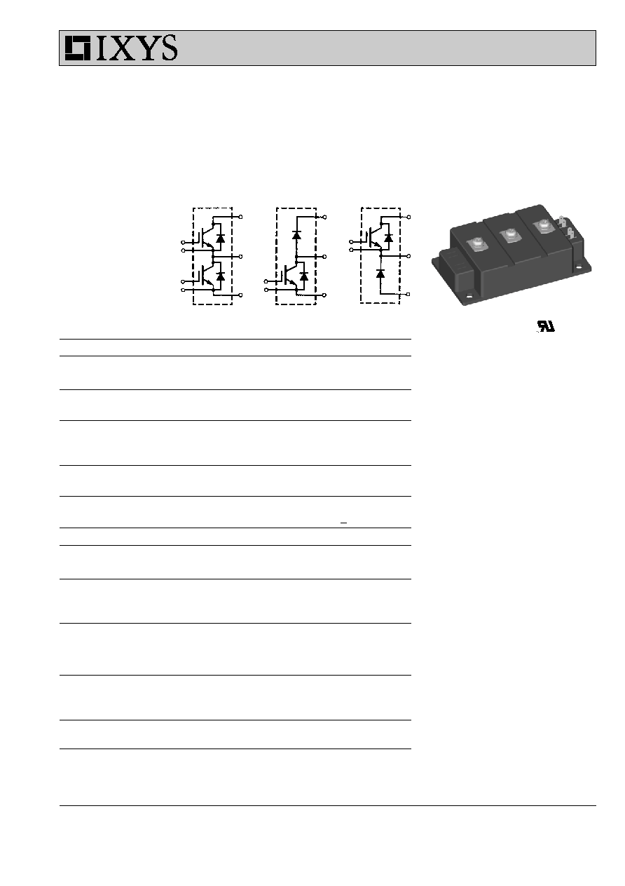
MII 300-12 A4
MID 300-12 A4
MDI 300-12 A4
Symbol
Conditions
Maximum Ratings
V
CES
T
J
= 25
°
C to 150
°
C
1200
V
V
CGR
T
J
= 25
°
C to 150
°
C; R
GE
= 20 k
W
1200
V
V
GES
Continuous
±
20
V
V
GEM
Transient
±
30
V
I
C25
T
C
= 25
°
C
330
A
I
C80
T
C
= 80
°
C
220
A
I
CM
T
C
= 80
°
C, t
p
= 1 ms
440
A
t
SC
V
GE
= ±15 V, V
CE
= V
CES
, T
J
= 125
°
C
10
m
s
(SCSOA)
R
G
= 3.3
W
, non repetitive
RBSOA
V
GE
= ±15 V, T
J
= 125
°
C, R
G
= 3.3
W
I
CM
= 400
A
Clamped inductive load, L = 100
m
H
V
CEK
< V
CES
P
tot
T
C
= 25
°
C
1380
W
T
J
150
°
C
T
stg
-40 ... +150
°
C
V
ISOL
50/60 Hz, RMS
t = 1 min
4000
V~
I
ISOL
Ł
1 mA
t = 1 s
4800
V~
Insulating material: Al
2
O
3
M
d
Mounting torque (module)
2.25-2.75
Nm
20-25
lb.in.
(teminals)
2.5-3.7
Nm
22-33
lb.in.
d
S
Creepage distance on surface
10
mm
d
A
Strike distance through air
9.6
mm
a
Max. allowable acceleration
50
m/s
2
Weight
Typical
250
g
8.8
oz.
Data according to a single IGBT/FRED unless otherwise stated.
8
9
1
2
3
11
10
10
11
9
8
2
1
3
MII
2
1
3
10
11
MID
2
1
3
9
8
MDI
E 72873
I
C25
= 330 A
V
CES
= 1200 V
V
CE(sat) typ.
= 2.2 V
Features
q
NPT IGBT technology
q
low saturation voltage
q
low switching losses
q
switching frequency up to 30 kHz
q
square RBSOA, no latch up
q
high short circuit capability
q
positive temperature coefficient for
easy parallelling
q
MOS input, voltage controlled
q
ultra fast free wheeling diodes
q
package with DCB ceramic base plate
q
isolation voltage 4800 V
q
UL registered E72873
Advantages
q
space and weight savings
q
reduced protection circuits
Typical Applications
q
AC and DC motor control
q
AC servo and robot drives
q
power supplies
q
welding inverters
030

© 2000 IXYS All rights reserved
2 - 4
MII 300-12 A4
MID 300-12 A4
MDI 300-12 A4
Symbol
Conditions
Characteristic Values
(T
J
= 25
°
C, unless otherwise specified)
min.
typ.
max.
V
(BR)CES
V
GE
= 0 V
1200
V
V
GE(th)
I
C
= 8 mA, V
CE
= V
GE
4.5
6.5
V
I
CES
V
CE
= V
CES
T
J
= 25
°
C
13 mA
T
J
= 125
°
C
20
mA
I
GES
V
CE
= 0 V, V
GE
=
±
20 V
±
800
nA
V
CE(sat)
I
C
= 200 A, V
GE
= 15 V
2.2
2.7
V
C
ies
13
nF
C
oes
V
CE
= 25 V, V
GE
= 0 V, f = 1 MHz
2
nF
C
res
1
nF
t
d(on)
100
ns
t
r
60
ns
t
d(off)
600
ns
t
f
90
ns
E
on
32
mJ
E
off
29
mJ
R
thJC
0.09 K/W
R
thJS
with heatsink compound
0.18
K/W
Reverse Diode (FRED)
Characteristic Values
(T
J
= 25
°
C, unless otherwise specified)
min.
typ.
max.
V
F
I
F
= 200 A, V
GE
= 0 V,
2.2
2.5
V
I
F
= 200 A, V
GE
= 0 V, T
J
= 125
°
C
1.7
2.3
V
I
F
T
C
= 25
°
C
450
A
T
C
= 80
°
C
280
A
I
RM
I
F
= 200 A, V
GE
= 0 V, -di
F
/dt = 1800 A/
m
s
180
A
t
rr
T
J
= 125
°
C, V
R
= 600 V
200
ns
R
thJC
0.15 K/W
R
thJS
with heatsink compound
0.3
K/W
Inductive load, T
J
= 125
°
C
I
C
= 200 A, V
GE
= ±15 V
V
CE
= 600 V, R
G
= 3.3
W
Dimensions in mm (1 mm = 0.0394")
Equivalent Circuits for Simulation
Conduction
IGBT (typ. at V
GE
= 15 V; T
J
= 125°C)
V
0
= 1.3 V; R
0
= 6.2 mW
Free Wheeling Diode (typ. at T
J
= 125°C)
V
0
= 1.3 V; R
0
= 2.4 mW
Thermal Response
IGBT (typ.)
C
th1
= 0.50 J/K; R
th1
= 0.088 K/W
C
th2
= 1.16 J/K; R
th2
= 0.002 K/W
Free Wheeling Diode (typ.)
C
th1
= 0.44 J/K; R
th1
= 0.146 K/W
C
th2
= 0.80 J/K; R
th2
= 0.003 K/W
© 2000 IXYS All rights reserved
3 - 4
0
200
400
600
800
1000
0
40
80
120
0
100
200
300
0
1
2
3
4
0
100
200
300
400
500
600
700
800
900
0.0
0.5
1.0
1.5
2.0
2.5
3.0
0
100
200
300
400
500
0
200
400
600
800
1000
0
5
10
15
20
0.0
0.5
1.0
1.5
2.0
2.5
3.0
3.5
0
100
200
300
400
500
13V
11V
T
J
= 25°C
V
GE
=17V
T
J
= 125°C
V
CE
= 600V
I
C
= 200A
15V
5
6
7
8
9
10
11
0
100
200
300
400
500
13V
11V
V
GE
=17V
15V
V
CE
= 20V
T
J
= 25°C
9V
9V
V
CE
V
A
I
C
V
CE
A
I
C
V
V
V
V
GE
V
F
A
I
C
A
I
F
nC
Q
G
-di/dt
V
V
GE
A
I
RM
t
rr
ns
A/
m
s
300-12
T
J
= 125°C
V
R
= 600V
I
F
= 200A
T
J
= 25°C
T
J
= 125°C
I
RM
t
rr
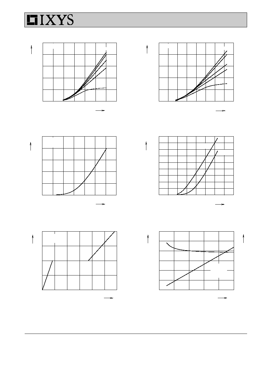
Fig. 1
Typ. output characteristics
Fig. 2 Typ. output characteristics
Fig. 3
Typ. transfer characteristics
Fig. 4 Typ. forward characteristics of
free wheeling diode
Fig. 5
Typ. turn on gate charge
Fig. 6 Typ. turn off characteristics of
free wheeling diode
MII 300-12 A4
MID 300-12 A4
MDI 300-12 A4
© 2000 IXYS All rights reserved
4 - 4
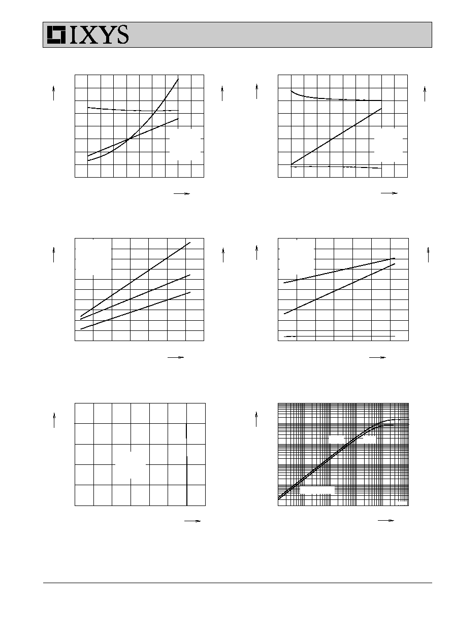
Fig. 7
Typ. turn on energy and switching
Fig. 8 Typ. turn off energy and switching
times versus collector current
times versus collector current
Fig. 9
Typ. turn on energy and switching
Fig.10 Typ. turn off energy and switching
times versus gate resistor
times versus gate resistor
Fig. 11 Reverse biased safe operating area
Fig. 12 Typ. transient thermal impedance
RBSOA
0
100
200
300
400
500
0
20
40
60
80
0
40
80
120
160
0
100
200
300
400
500
0
20
40
60
80
0
200
400
600
800
0.00001
0.0001
0.001
0.01
0.1
1
0.00001
0.0001
0.001
0.01
0.1
1
0
4
8
12
16
20
24
28
0
10
20
30
40
50
0
400
800
1200
1600
2000
0
4
8
12
16
20
24
28
0
20
40
60
80
100
0
80
160
240
320
400
single pulse
V
CE
= 600V
V
GE
= ±15V
R
G
= 3.3
W
T
J
= 125°C
300-12
V
CE
= 600V
V
GE
= ±15V
I
C
= 200A
T
J
= 125°C
0
200
400
600
800
1000 1200
0
100
200
300
400
500
R
G
= 3.3
W
T
J
= 125°C
V
CEK
< V
CES
V
CE
= 600V
V
GE
= ±15V
R
G
= 3.3
W
T
J
= 125°C
E
on
V
CE
= 600V
V
GE
= ±15V
I
C
= 200A
T
J
= 125°C
t
d(on)
t
r
E
off
t
d(off)
t
f
E
on
t
d(on)
t
r
E
off
t
d(off)
t
f
I
C
A
I
C
A
mJ
E
off
mJ
E
on
ns
t
ns
t
R
G
W
R
G
W
V
CE
t
s
mJ
E
on
mJ
E
off
ns
t
ns
t
I
CM
K/W
Z
thJC
IGBT
diode
V
A
MII 300-12 A4
MID 300-12 A4
MDI 300-12 A4