1 - 4
© 2000 IXYS All rights reserved
Symbol
Test Conditions
Maximum Ratings
V
DSS
T
J
= 25
°
C to 150
°
C
200
V
V
DGR
T
J
= 25
°
C to 150
°
C; R
GS
= 1 M
200
V
V
GS
Continuous
±
20
V
V
GSM
Transient
±
30
V
I
D25
T
C
= 25
°
C
50
A
I
DM
T
C
= 25
°
C, pulse width limited by T
JM
200
A
P
D
T
C
= 25
°
C
300
W
T
J
-55 ... +150
°
C
T
JM
150
°
C
T
stg
-55 ... +150
°
C
M
d
Mounting torque
1.13/10
Nm/lb.in.
Weight
TO-204 = 18 g, TO-247 = 6 g
Maximum lead temperature for soldering
300
°
C
1.6 mm (0.062 in.) from case for 10 s
TO-247 AD (IXTH)
MegaMOS
TM
FET
N-Channel Enhancement Mode
TO-204 AE (IXTM)
G = Gate,
D = Drain,
S = Source,
TAB = Drain
D
G
Symbol
Test Conditions
Characteristic Values
(T
J
= 25
°
C, unless otherwise specified)
min.
typ.
max.
V
DSS
V
GS
= 0 V, I
D
= 250
µ
A
200
V
V
GS(th)
V
DS
= V
GS
, I
D
= 250
µ
A
2
4
V
I
GSS
V
GS
=
±
20 V
DC
, V
DS
= 0
±
100
nA
I
DSS
V
DS
= 0.8 · V
DSS
T
J
= 25
°
C
200
µ
A
V
GS
= 0 V
T
J
= 125
°
C
1
mA
R
DS(on)
V
GS
= 10 V, I
D
= 0.5 I
D25
0.045
Pulse test, t
300
µ
s, duty cycle d
2 %
Features
l
International standard packages
l
Low R
DS (on)
HDMOS
TM
process
l
Rugged polysilicon gate cell structure
l
Low package inductance (< 5 nH)
- easy to drive and to protect
l
Fast switching times
Applications
l
Switch-mode and resonant-mode
power supplies
l
Motor controls
l
Uninterruptible Power Supplies (UPS)
l
DC choppers
Advantages
l
Easy to mount with 1 screw (TO-247)
(isolated mounting screw hole)
l
Space savings
l
High power density
91534F(5/97)
D (TAB)
IXTH 50N20
V
DSS
= 200 V
IXTM 50N20
I
D25
= 50 A
R
DS(on)
= 45 m
IXYS reserves the right to change limits, test conditions, and dimensions.

2 - 4
© 2000 IXYS All rights reserved
IXTH 50N20
IXTM 50N20
Symbol
Test Conditions
Characteristic Values
(T
J
= 25
°
C, unless otherwise specified)
min.
typ.
max.
g
fs
V
DS
= 10 V; I
D
= 0.5 · I
D25
, pulse test
20
32
S
C
iss
4600
pF
C
oss
V
GS
= 0 V, V
DS
= 25 V, f = 1 MHz
800
pF
C
rss
285
pF
t
d(on)
18
25
ns
t
r
V
GS
= 10 V, V
DS
= 0.5 · V
DSS
, I
D
= 0.5 I
D25
15
20
ns
t
d(off)
R
G
= 2
,
(External)
72
90
ns
t
f
16
25
ns
Q
g(on)
190
220
nC
Q
gs
V
GS
= 10 V, V
DS
= 0.5 · V
DSS
, I
D
= 0.5 I
D25
35
50
nC
Q
g d
95
110
nC
R
thJC
0.42
K/W
R
thCK
0.25
K/W
Source-Drain Diode
Characteristic Values
(T
J
= 25
°
C, unless otherwise specified)
Symbol
Test Conditions
min.
typ.
max.
I
S
V
GS
= 0 V
50N20
50
A
I
SM
Repetitive;
200
A
pulse width limited by T
JM
V
SD
I
F
= I
S
, V
GS
= 0 V,
1.5
V
Pulse test, t
300
µ
s, duty cycle d
2 %
t
rr
I
F
= I
S
, -di/dt = 100 A/
µ
s, V
R
= 100 V
400
ns
Dim.
Millimeter
Inches
Min.
Max.
Min.
Max.
A
4.7
5.3
.185
.209
A
1
2.2
2.54
.087
.102
A
2
2.2
2.6
.059
.098
b
1.0
1.4
.040
.055
b
1
1.65
2.13
.065
.084
b
2
2.87
3.12
.113
.123
C
.4
.8
.016
.031
D
20.80
21.46
.819
.845
E
15.75
16.26
.610
.640
e
5.20
5.72
0.205 0.225
L
19.81
20.32
.780
.800
L1
4.50
.177
P
3.55
3.65
.140
.144
Q
5.89
6.40
0.232 0.252
R
4.32
5.49
.170
.216
S
6.15 BSC
242 BSC
TO-247 AD (IXTH) Outline
Dim.
Millimeter
Inches
Min.
Max.
Min.
Max.
A
6.4
11.4
.250
.450
A1
1.53
3.42
.060
.135
b
1.45
1.60
.057
.063
D
22.22
.875
e
10.67
11.17
.420
.440
e1
5.21
5.71
.205
.225
L
11.18
12.19
.440
.480
p
3.84
4.19
.151
.165
p 1 3.84
4.19
.151
.165
q
30.15 BSC
1.187 BSC
R
12.58
13.33
.495
.525
R 1
3.33
4.77
.131
.188
s
16.64
17.14
.655
.675
TO-204AE (IXTM) Outline
Terminals: 1 - Gate
2 - Drain
3 - Source
Tab - Drain
Pins
1 - Gate
2 - Source
Case - Drain
1 2 3
IXYS MOSFETS and IGBTs are covered by one or more of the following U.S. patents:
4,835,592
4,881,106
5,017,508
5,049,961
5,187,117
5,486,715
4,850,072
4,931,844
5,034,796
5,063,307
5,237,481
5,381,025
3 - 4
© 2000 IXYS All rights reserved
T
J
- Degrees C
-50
-25
0
25
50
75
100 125 150
BV/
V
G(
t
h
)
- N
o
r
m
a
lize
d
0.5
0.6
0.7
0.8
0.9
1.0
1.1
1.2
V
GS(th)
BV
CES
T
C
- Degrees C
-50
-25
0
25
50
75
100 125 150
I
D
-
Am
per
es
0
10
20
30
40
50
60
70
80
42N20
50N20
T
J
- Degrees C
-50
-25
0
25
50
75
100 125 150
R
DS
(on)
- No
rm
a
l
i
z
e
d
0.75
1.00
1.25
1.50
1.75
2.00
2.25
2.50
I
D
- Amperes
0
25
50
75
100 125 150 175 200
R
DS
(
on)
- m
O
h
m
s
25
50
75
100
125
V
GS
- Volts
0
1
2
3
4
5
6
7
8
9
10
I
D
-
Am
per
es
0
10
20
30
40
50
60
70
80
90
100
V
DS
- Volts
0
1
2
3
4
5
6
7
8
9
10
I
D
-
Am
per
es
0
10
20
30
40
50
60
70
80
90
100
6V
5V
T
J
= 25°C
V
GS
= 10V
9V
8V
7V
T
J
= 25°C
T
J
= 25°C
V
GS
= 15V
V
GS
= 10V
I
D
= 40A
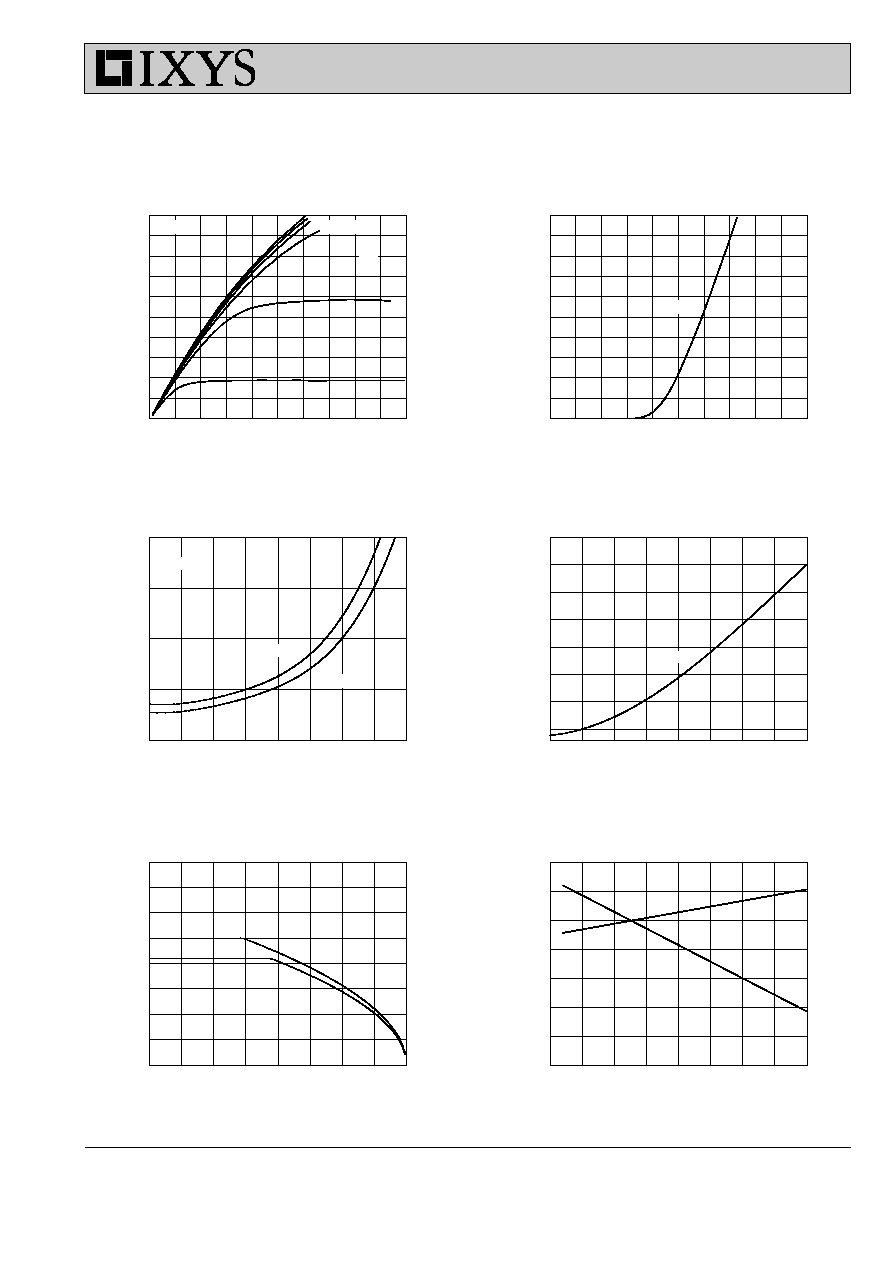
Fig. 1 Output Characteristics
Fig. 2 Input Admittance
Fig. 3 R
DS(on)
vs. Drain Current
Fig. 4 Temperature Dependence
of Drain to Source Resistance
Fig. 5 Drain Current vs.
Fig. 6 Temperature Dependence of
Case Temperature
Breakdown and Threshold Voltage
IXTH 50N20
IXTM 50N20
4 - 4
© 2000 IXYS All rights reserved
IXTH 50N20
IXTM 50N20
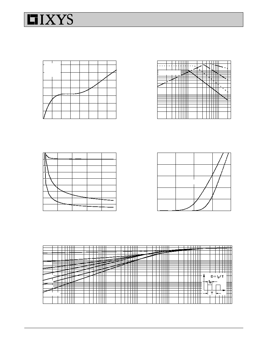
Fig.7 Gate Charge Characteristic Curve
Fig.8 Forward Bias Safe Operating Area
Fig.11 Transient Thermal Impedance
Fig.9 Capacitance Curves
Fig.10 Source Current vs. Source
to Drain Voltage
T
J
= 25°C
Gate Charge - nCoulombs
0
25
50
75
100 125 150 175 200
V
GE
- V
o
lts
0
2
4
6
8
10
12
14
Time - Seconds
0.00001
0.0001
0.001
0.01
0.1
1
10
T
her
m
a
l
R
e
spons
e -
K/
W
0.001
0.01
0.1
V
DS
- Volts
0
5
10
15
20
25
C
apaci
t
ance -
pF
0
500
1000
1500
2000
2500
3000
3500
4000
4500
C
iss
C
oss
C
rss
10ms
100ms
V
DS
- Volts
1
10
100
I
D
-
Am
per
es
1
10
100
V
SD
- Volts
0.2
0.4
0.6
0.8
1.0
I
D
-
A
m
per
es
0
10
20
30
40
50
V
DS
= 100V
I
D
= 50A
I
G
= 10mA
Limited by R
DS(on)
10µs
100µs
1ms
f = 1 MHz
V
DS
= 25V
T
J
= 125°C
D=0.01
D=0.02
D=0.05
D=0.1
D=0.2
D=0.5
Single pulse