1 - 4
© 2000 IXYS All rights reserved
Symbol
Test Conditions
Characteristic Values
(T
J
= 25°C unless otherwise specified)
Min.
Typ.
Max.
V
DSS
V
GS
= 0 V, I
D
= 5 mA
500
V
BV
DSS
temperature coefficient
0.087
%/K
V
GS(th)
V
DS
= V
GS
,
I
D
= 250
µ
A
2.0
4.0
V
V
GS(th)
temperature coefficient
-0.25
%/K
I
GSS
V
GS
=
±
20 V DC, V
DS
= 0
±
100
nA
I
DSS
V
DS
= 0.8 V
DSS
T
J
= 25°C
200
µ
A
V
GS
= 0 V
T
J
= 125°C
3
mA
R
DS(on)
V
GS
= 10 V, I
D
= 0.5 I
D25
0.17
Symbol
Test conditions
Maximum ratings
V
DSS
T
J
= 25°C to 150°C
500
V
V
DGR
T
J
= 25°C to 150°C; R
GS
= 1.0 M
500
V
V
GS
Continuous
±20
V
V
GSM
Transient
±30
V
I
D25
T
C
= 25°C
33
A
I
DM
T
C
= 25°C, pulse width limited by T
JM
132
A
P
D
T
C
= 25°C
416
W
T
J
-55 ... +150
°C
T
JM
150
°C
T
stg
-55 ... +150
°C
M
d
Mounting torque
1.13/10 Nm/lb.in.
Weight
10
g
Max lead temperature for soldering
300
°
C
1.6 mm (0.062 in.) from case for 10 s
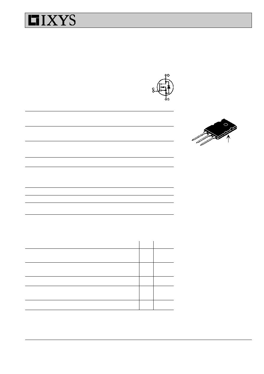
N-Channel Enhancement Mode
S
G
D
G = Gate
D = Drain
S = Source
TAB = Drain
TO-264 AA
95513C (4/97)
Features
· Low R
DS (on)
HDMOS
TM
process
· Rugged polysilicon gate cell
structure
· International standard package
· Fast switching times
Applications
· Motor controls
· DC choppers
· Uninterruptable Power Supplies
(UPS)
· Switch-mode and resonant-mode
Advantages
· Easy to mount with one screw
(isolated mounting screw hole)
· Space savings
· High power density
Preliminary data
D (TAB)
IXTK 33N50
V
DSS
= 500 V
I
D (cont)
= 33 A
R
DS(on)
= 0.17
High Current
MegaMOS
TM
FET
IXYS reserves the right to change limits, test conditions, and dimensions.

2 - 4
© 2000 IXYS All rights reserved
IXTK 33N50
Symbol
Test Conditions
Characteristic values
(T
J
= 25°C unless otherwise specified)
Min.
Typ. Max.
g
fs
V
DS
= 10 V; I
D
= 0.5 I
D25
, pulse test
24
S
C
iss
4900
pF
C
oss
V
GS
= 0 V, V
DS
= 25 V, f = 1 MHz
690
pF
C
rss
300
pF
t
d(on)
53
ns
t
r
V
GS
= 10 V, V
DS
= 0.5 V
DSS
, I
D
= 0.5 I
D25
30
ns
t
d(off)
R
G
= 1
(External)
140
ns
t
f
40
ns
Q
g(on)
250
nC
Q
gs
V
GS
= 10 V, V
DS
= 0.5 V
DSS
, I
D
= 0.5 I
D25
30
nC
Q
g d
115
nC
R
thJC
0.30 K/W
R
thCK
0.15
K/W
Source-Drain Diode
Ratings and Characteristics
(T
J
= 25°C unless otherwise specified)
Symbol
Test Conditions
Min.
Typ.
Max.
I
S
V
GS
= 0 V
33
A
I
SM
Repetitive; pulse width limited by T
JM
132
A
V
SD
I
F
= I
S
, V
GS
= 0 V,
1.5
V
Pulse test, t
300 µs, duty cycle d
2 %
t
rr
I
F
= I
S
, -di/dt = 100 A/µs, V
R
= 100 V
850
ns
TO-264 AA Outline
Millimeter
Inches
Min.
Max.
Min.
Max.
A
4.82
5.13
.190
.202
A1
2.54
2.89
.100
.114
A2
2.00
2.10
.079
.083
b
1.12
1.42
.044
.056
b1
2.39
2.69
.094
.106
b2
2.90
3.09
.114
.122
c
0.53
0.83
.021
.033
D
25.91
26.16
1.020
1.030
E
19.81
19.96
.780
.786
e
5.46 BSC
.215 BSC
J
0.00
0.25
.000
.010
K
0.00
0.25
.000
.010
L
20.32
20.83
.800
.820
L1
2.29
2.59
.090
.102
P
3.17
3.66
.125
.144
Q
6.07
6.27
.239
.247
Q1
8.38
8.69
.330
.342
R
3.81
4.32
.150
.170
R1
1.78
2.29
.070
.090
S
6.04
6.30
.238
.248
T
1.57
1.83
.062
.072
Dim.
IXYS MOSFETS and IGBTs are covered by one or more of the following U.S. patents:
4,835,592
4,881,106
5,017,508
5,049,961
5,187,117
5,486,715
4,850,072
4,931,844
5,034,796
5,063,307
5,237,481
5,381,025
3 - 4
© 2000 IXYS All rights reserved
V
GS
- Volts
2
3
4
5
6
7
8
I
D
- A
m
p
e
r
e
s
0
10
20
30
40
50
T
C
- Degrees C
-50 -25
0
25
50
75
100 125 150
I
D
- A
m
p
e
re
s
0
5
10
15
20
25
30
35
40
T
J
- Degrees C
25
50
75
100
125
150
R
DS
(
O
N
)
-
Norm
al
i
z
ed
1.0
1.5
2.0
2.5
3.0
3.5
4.0
4.5
5.0
5.5
I
D
= 16.5 A
I
D
- Amperes
0
10
20
30
40
50
60
70
80
R
DS
(
O
N
)
-
N
o
rm
al
i
z
ed
0.8
1.0
1.2
1.4
1.6
1.8
2.0
2.2
2.4
2.6
2.8
3.0
V
DS
- Volts
0
4
8
12
16
20
I
D
- A
m
p
e
re
s
0
10
20
30
40
50
V
DS
- Volts
0
4
8
12
16
20
I
D
- A
m
p
e
r
e
s
0
10
20
30
40
50
60
70
80
6V
5V
T
J
= 25°C
V
GS
= 10 V
V
GS
= 10 V
9 V
8 V
T
J
= 125°C
V
GS
= 10 V
T
J
= 25°C
7V
6V
5V
T
J
= 25
o
C
I
D
= 33 A
T
J
= 125°C
T
J
= 125
o
C
V
GS
= 10 V
9 V
8 V
7 V
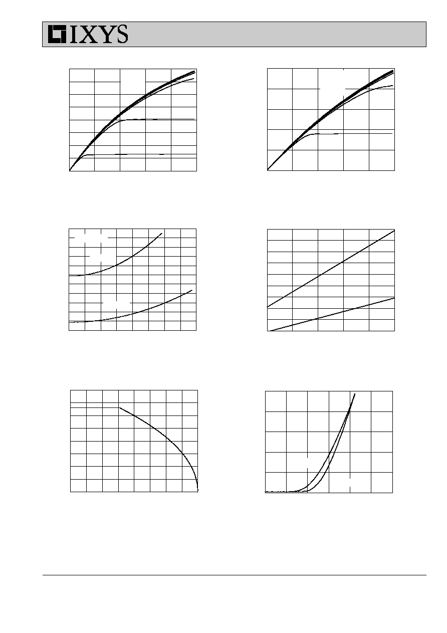
Figure 1. Output Characteristics at 25
O
C
Figure 2. Output Characteristics at 125
O
C
Figure 3. R
DS(on)
normalized to 16.5A/25
O
C vs. I
D
Figure 5. Drain Current vs. Case Temperature
Figure 6. Admittance Curves
Figure 4. R
DS(on)
normalized to 16.5A/25
O
C vs. T
J
IXTK 33N50
4 - 4
© 2000 IXYS All rights reserved
V
DS
- Volts
1 0
1 00
I
D
- A
m
p
e
r
e
s
0. 1
1
1 0
1 00
Pulse Width - Seconds
0.001
0.01
0.1
1
10
R(
th
)
JC
- K/
W
0.01
0.10
1.00
V
DS
- Volts
0
5
10
15
20
25
C
a
pac
i
t
a
nce -
pF
0
500
1000
1500
2000
2500
3000
3500
4000
4500
V
SD
- Volts
0.4
0.6
0.8
1.0
1.2
I
D
- A
m
p
e
r
e
s
0
20
40
60
80
100
Gate Charge - nC
0
50
100
150
200
250
300
V
GS
- Vo
lt
s
0
2
4
6
8
10
12
14
Vds=300V
I
D
=30A
I
G
=10mA
F = 1MHz
C
rss
C
oss
C
iss
T
J
= 125°C
T
J
= 25°C
V
ds
= 300 V
I
D
= 33 A
I
G
= 10 mA
F = 1 MHz
T
C
= 25°C
10 ms
1 ms
100 ms
DC
500
Single Pulse
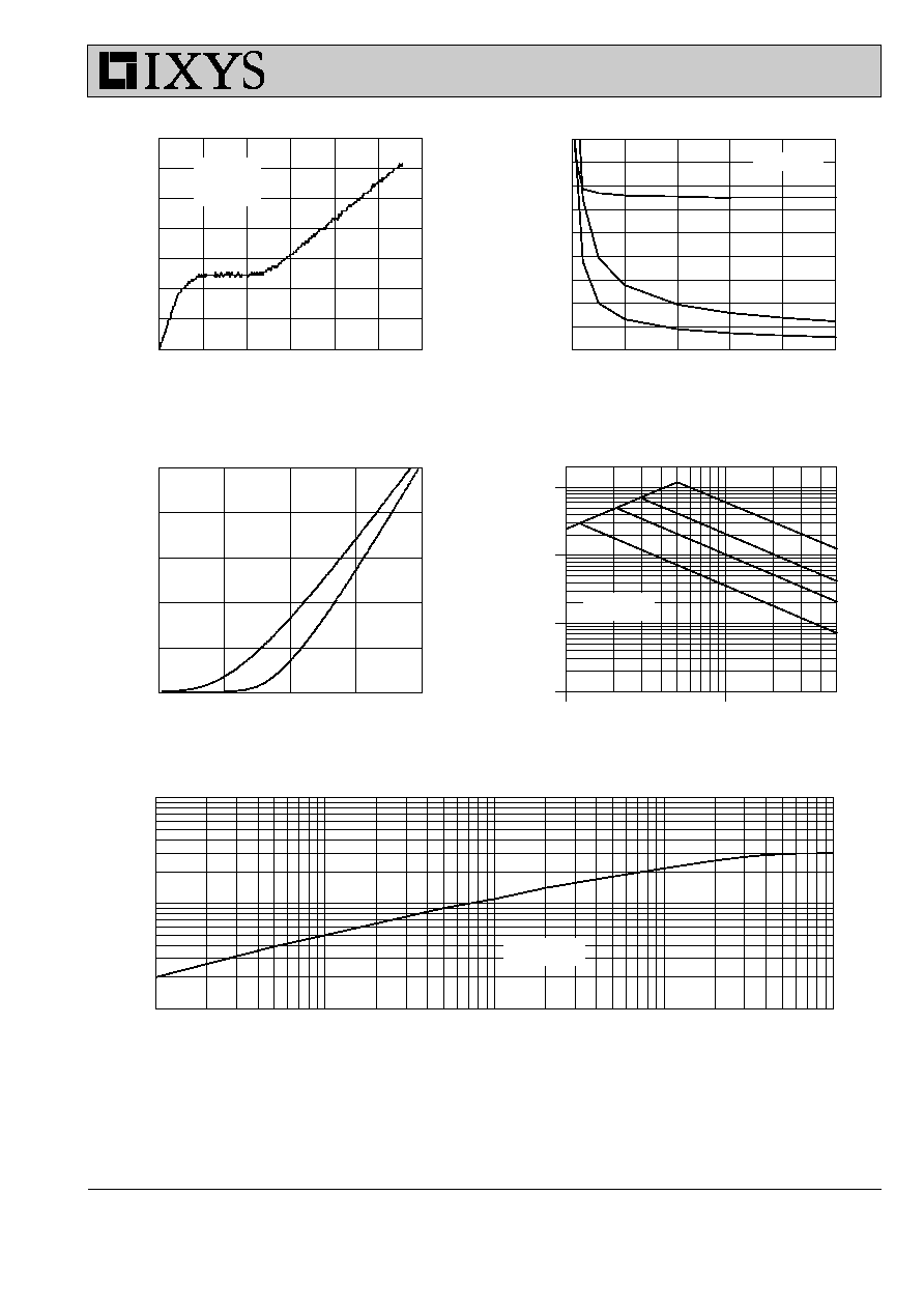
Figure 7. Gate Charge
Figure 8. Capacitance Curves
Figure 11. Transient Thermal Resistance
Figure 10. Forward Biased SOA
Figure 9. Source Current vs. Source-to-
Drain Voltage
IXTK 33N50