DS98905C(IXTH-IXTT50P10)
© 2004 IXYS All rights reserved
Symbol
Test Conditions
Maximum Ratings
V
DSS
T
J
= 25
°C to 150°C
-100
V
V
DGR
T
J
= 25
°C to 150°C; R
GS
= 1 M
-100
V
V
GS
Continuous
±20
V
V
GSM
Transient
±30
V
I
D25
T
C
= 25
°C
-50
A
I
DM
T
C
= 25
°C, pulse width limited by T
J
-200
A
I
AR
T
C
= 25
°C
-50
A
E
AR
T
C
= 25
°C
30
mJ
P
D
T
C
= 25
°C
300
W
T
J
-55 ... +150
°C
T
JM
150
°C
T
stg
-55 ... +150
°C
T
L
Maximum lead temperature for soldering
300
°C
1.6 mm (0.062 in.) from case for 10 s
M
d
Mounting torque (TO-247)
1.13/10 Nm/lb.in.
Weight
(TO-247)
6
g
(TO-268)
4
g
V
DSS
= -100 V
I
D25
= -50 A
R
DS(on)
= 55 m
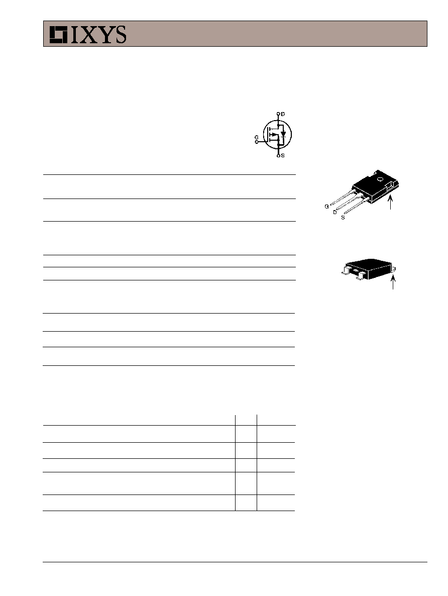
TO-247 AD (IXTH)
G = Gate,
D = Drain,
S = Source,
TAB = Drain
D (TAB)
Symbol
Test Conditions
Characteristic Values
(T
J
= 25
°C, unless otherwise specified)
min.
typ. max.
V
DSS
V
GS
= 0 V, I
D
= -250
µA
-100
V
V
GS(th)
V
DS
= V
GS
, I
D
= -250
µA
-3.0
-5.0
V
I
GSS
V
GS
=
±20 V
DC
, V
DS
= 0
±100
nA
I
DSS
V
DS
= 0.8 · V
DSS
T
J
= 25
°C
-25
µA
V
GS
= 0 V
T
J
= 125
°C
-1
mA
R
DS(on)
V
GS
= -10 V, I
D
= 0.5 · I
D25
55
m
Features
·
International standard package
JEDEC TO-247 AD
·
Low R
DS (on)
HDMOS
TM
process
·
Rugged polysilicon gate cell structure
·
Unclamped Inductive Switching (UIS)
rated
·
Low package inductance (<5 nH)
- easy to drive and to protect
Applications
·
High side switching
·
Push-pull amplifiers
·
DC choppers
·
Automatic test equipment
Advantages
·
Easy to mount with 1 screw
(isolated mounting screw hole)
·
Space savings
·
High power density
DS98905D(10/04)
P-Channel Enhancement Mode
Avalanche Rated
Standard Power MOSFET
IXTH 50P10
IXTT 50P10
TO-268 (IXTT)
G
S
D (TAB)
IXYS reserves the right to change limits, test conditions, and dimensions.
IXTH 50P10
IXTT 50P10
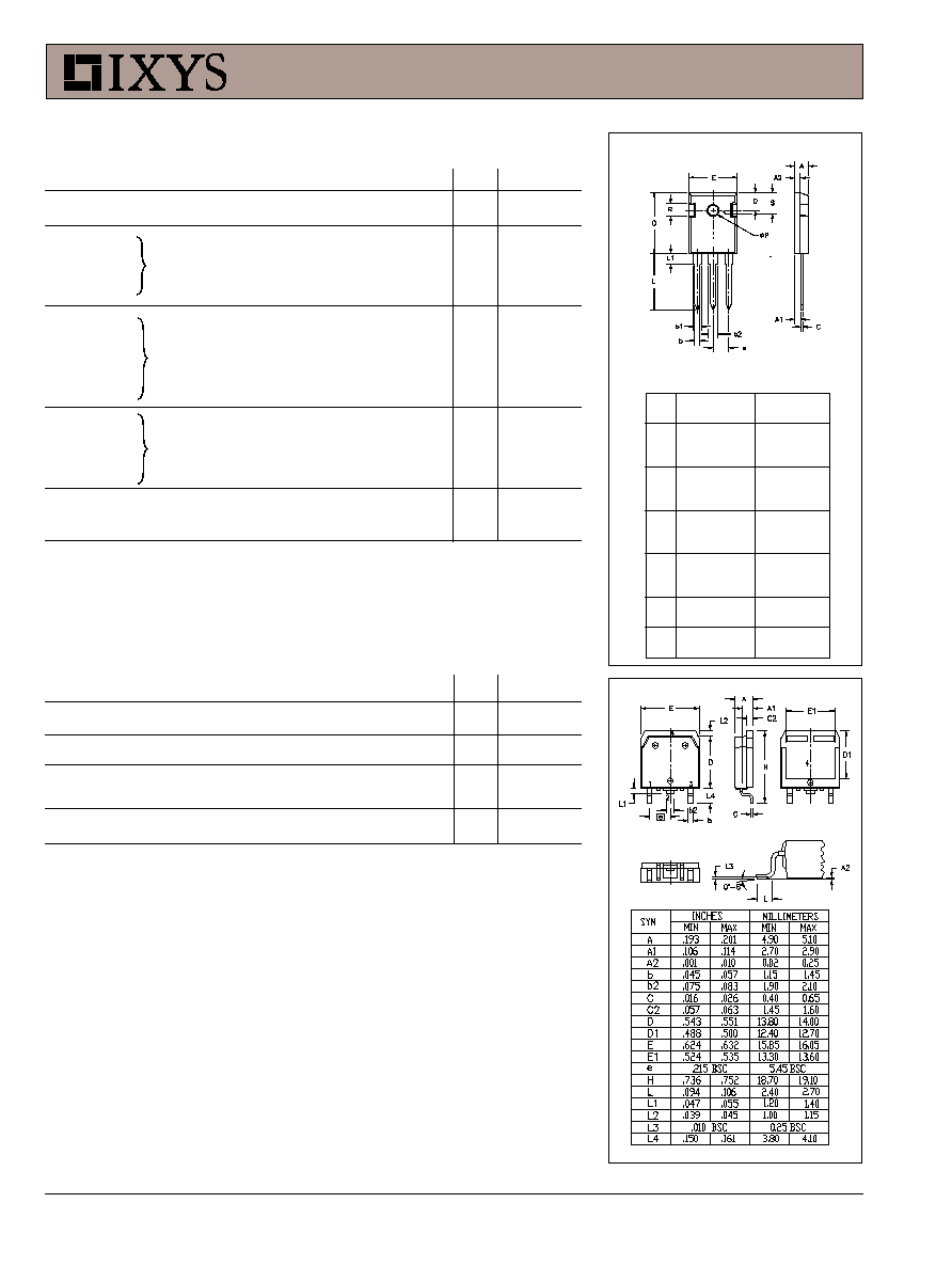
Dim.
Millimeter
Inches
Min.
Max.
Min. Max.
A
4.7
5.3
.185
.209
A
1
2.2
2.54
.087
.102
A
2
2.2
2.6
.059
.098
b
1.0
1.4
.040
.055
b
1
1.65
2.13
.065
.084
b
2
2.87
3.12
.113
.123
C
.4
.8
.016
.031
D
20.80
21.46
.819
.845
E
15.75
16.26
.610
.640
e
5.20
5.72
0.205 0.225
L
19.81
20.32
.780
.800
L1
4.50
.177
P
3.55
3.65
.140
.144
Q
5.89
6.40
0.232 0.252
R
4.32
5.49
.170
.216
S
6.15 BSC
242 BSC
TO-247 AD Outline
Terminals: 1 - Gate
2 - Drain
3 - Source
Tab - Drain
1 2 3
Symbol
Test Conditions
Characteristic Values
(T
J
= 25
°C, unless otherwise specified)
min.
typ.
max.
g
fs
V
DS
= -10 V; I
D
= I
D25
, pulse test
8
16
S
C
iss
4200
pF
C
oss
V
GS
= 0 V, V
DS
= -25 V, f = 1 MHz
1720
pF
C
rss
750
pF
t
d(on)
46
ns
t
r
V
GS
= -10 V, V
DS
= 0.5 V
DSS
, I
D
= 0.5 I
D25
39
ns
t
d(off)
R
G
= 4.7
(External)
86
ns
t
f
38
ns
Q
g(on)
140
nC
Q
gs
V
GS
= -10 V, V
DS
= 0.5 V
DSS
, I
D
= 0.5 I
D25
36
nC
Q
gd
70
nC
R
thJC
0.42
K/W
R
thCS
(TO-247)
0.25
K/W
Source-Drain Diode
Characteristic Values
(T
J
= 25
°C, unless otherwise specified)
Symbol
Test Conditions
min.
typ.
max.
I
S
V
GS
= 0
-25
A
I
SM
Repetitive; pulse width limited by T
JM
-200
A
V
SD
I
F
= I
S
, V
GS
= 0 V,
-3
V
Pulse test, t
300 µs, duty cycle d 2 %
t
rr
I
F
= I
S
, di/dt = 100 A/
µs, V
R
= -50 V
180
ns
TO-268 Outline
IXYS MOSFETs and IGBTs are covered by
4,835,592
4,931,844
5,049,961
5,237,481
6,162,665
6,404,065 B1
6,683,344
6,727,585
one or moreof the following U.S. patents:
4,850,072
5,017,508
5,063,307
5,381,025
6,259,123 B1
6,534,343
6,710,405B2
6,759,692
4,881,106
5,034,796
5,187,117
5,486,715
6,306,728 B1
6,583,505
6,710,463
© 2004 IXYS All rights reserved
IXTH 50P10
IXTT 50P10
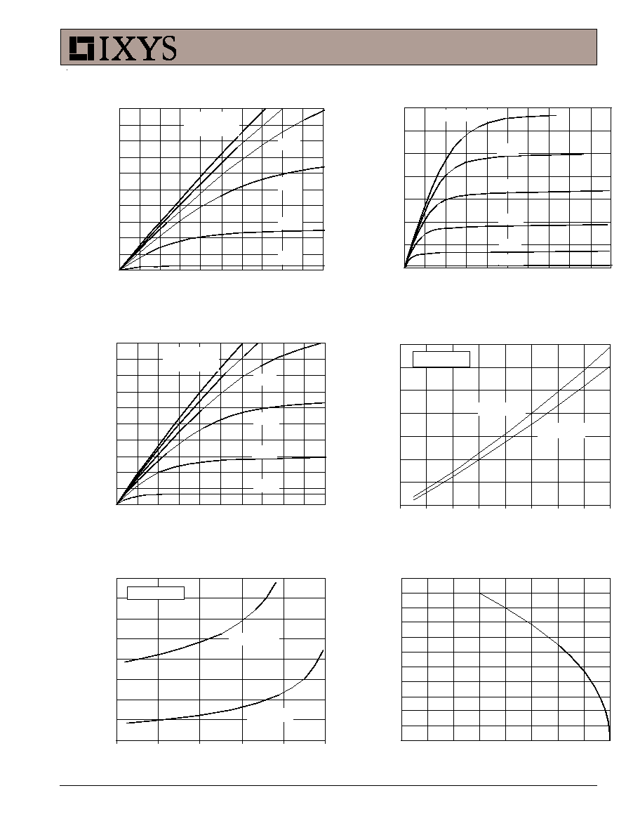
Fig. 2. Extended Output Characteristics
@ 25 deg. C
-140
-120
-100
-80
-60
-40
-20
0
-20
-18
-16
-14
-12
-10
-8
-6
-4
-2
0
V
D S
- Volts
I
D
-
A
m
per
es
V
GS
= -10V
-5V
-6V
-7V
-8V
-9V
Fig. 1. Output Characteristics
@ 25 Deg. C
-50
-45
-40
-35
-30
-25
-20
-15
-10
-5
0
-2.5
-2
-1.5
-1
-0.5
0
V
D S
- Volts
I
D
-
A
m
per
e
s
V
GS
= -10V
-9V
-5V
-6V
-7V
-8V
Fig. 4. R
DS(on)
Norm alized to I
D25
Value vs.
Junction Tem perature
0.6
0.8
1
1.2
1.4
1.6
1.8
2
-50
-25
0
25
50
75
100
125
150
T
J
- Degrees Centigrade
R
D S
(
o
n
)
-
N
o
r
m
a
liz
e
d
I
D
= -50A
I
D
= -25A
V
GS
= -10V
Fig. 6. Drain Current vs. Case
Tem perature
-55
-50
-45
-40
-35
-30
-25
-20
-15
-10
-5
0
-50
-25
0
25
50
75
100
125
150
T
C
- Degrees Centigrade
I
D
- A
m
p
e
re
s
Fig. 5. R
DS(on)
Norm alized to I
D25
Value vs. I
D
0.8
1
1.2
1.4
1.6
1.8
2
2.2
2.4
-125
-100
-75
-50
-25
0
I
D
- Amperes
R
D
S
(
on)
-
N
o
rm
a
l
i
z
e
d
T
J
= 125ºC
T
J
= 25ºC
V
GS
= -10V
Fig. 3. Output Characteristics
@ 125 Deg. C
-50
-45
-40
-35
-30
-25
-20
-15
-10
-5
0
-5
-4
-3
-2
-1
0
V
D S
- Volts
I
D
-
A
m
per
e
s
V
GS
= -10V
-9V
-5V
-6V
-7V
-8V
IXYS reserves the right to change limits, test conditions, and dimensions.
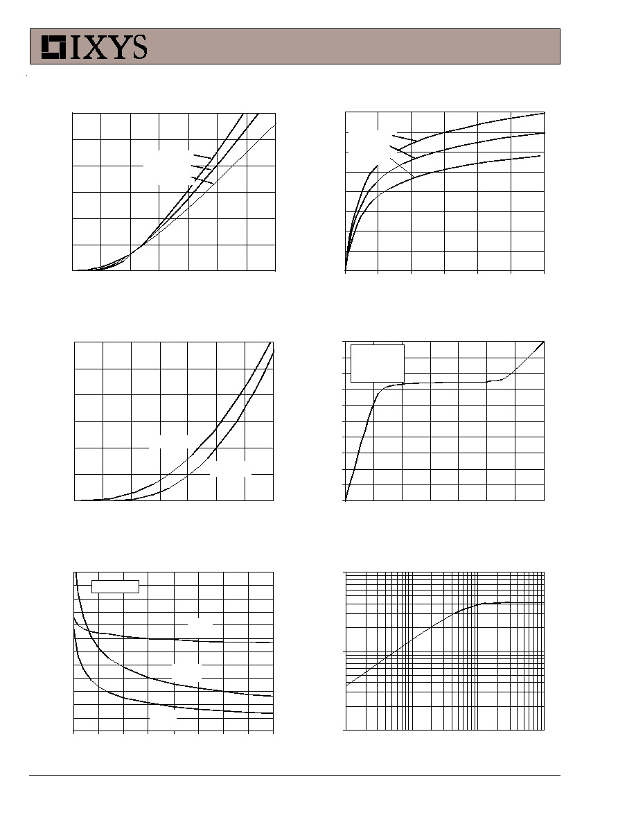
IXTH 50P10
IXTT 50P10
Fig. 11. Capacitance
0
1000
2000
3000
4000
5000
6000
-40
-35
-30
-25
-20
-15
-10
-5
0
V
D S
- Volts
C
apac
i
t
anc
e -
p
F
Ciss
Coss
Crss
f = 1MHz
Fig. 10. Gate Charge
-10
-9
-8
-7
-6
-5
-4
-3
-2
-1
0
0
20
40
60
80
100
120
140
Q
G
- nanoCoulombs
V
G S
-
V
o
l
t
s
V
DS
= -50V
I
D
= -25A
I
G
= -1mA
Fig. 7. Input Adm ittance
-150
-125
-100
-75
-50
-25
0
-11
-10
-9
-8
-7
-6
-5
-4
V
G S
- Volts
I
D
-
A
m
per
es
T
J
= -40ºC
25ºC
125ºC
Fig. 8. Transconductance
0
5
10
15
20
25
30
35
40
-150
-125
-100
-75
-50
-25
0
I
D
- Amperes
g
f s
-
S
i
em
ens
T
J
= -40ºC
25ºC
125ºC
Fig. 9. Source Current vs. Source-To-
Drain Voltage
-150
-125
-100
-75
-50
-25
0
-4
-3.5
-3
-2.5
-2
-1.5
-1
-0.5
V
S D
- Volts
I
S
-
A
m
per
es
T
J
= 125ºC
T
J
= 25ºC
Fig. 12. Maxim um Transient Therm al
Resistance
0.01
0.10
1.00
1
10
100
1000
Pulse Width - milliseconds
R
(t
h
)
J
C
-
(º
C
/
W
)