
1 - 4
© 2000 IXYS All rights reserved
Symbol
Test Conditions
Maximum Ratings
V
DSS
T
J
= 25
°
C to 150
°
C
1000
V
V
DGR
T
J
= 25
°
C to 150
°
C; R
GS
= 1 M
1000
V
V
GS
Continuous
±
20
V
V
GSM
Transient
±
30
V
I
D25
T
C
= 25
°
C
2
A
I
DM
T
C
= 25
°
C, pulse width limited by T
JM
8
A
P
D
T
C
= 25
°
C
100
W
T
J
-55 ... +150
°
C
T
JM
150
°
C
T
stg
-55 ... +150
°
C
M
d
Mounting torque
1.13/10
Nm/lb.in.
Weight
4
g
Maximum lead temperature for soldering
300
°
C
1.6 mm (0.062 in.) from case for 10 s
High Voltage
MOSFET
N-Channel Enhancement Mode
IXTA 2N100
IXTP 2N100
G = Gate,
D = Drain,
S = Source,
TAB = Drain
D (TAB)
Symbol
Test Conditions
Characteristic Values
(T
J
= 25
°
C, unless otherwise specified)
min.
typ.
max.
V
DSS
V
GS
= 0 V, I
D
= 250
µ
A
1000
V
V
GS(th)
V
DS
= V
GS
, I
D
= 250
µ
A
2
4.5
V
I
GSS
V
GS
=
±
20 V
DC
, V
DS
= 0
±
100
nA
I
DSS
V
DS
= 0.8 · V
DSS
T
J
= 25
°
C
200
µ
A
V
GS
= 0 V
T
J
= 125
°
C
1
mA
R
DS(on)
V
GS
= 10 V, I
D
= 0.5 I
D25
7.0
Pulse test, t
300
µ
s, duty cycle d
2 %
97540A(5/98)
G D
S
TO-220AB (IXTP)
V
DSS
= 1000 V
I
D25
= 2 A
R
DS(on)
= 7
TO-263 AA (IXTA)
Features
International standard packages
Low R
DS (on)
HDMOS
TM
process
Rugged polysilicon gate cell structure
Low package inductance (< 5 nH)
- easy to drive and to protect
Fast switching times
Applications
Switch-mode and resonant-mode
power supplies
Flyback inverters
DC choppers
Advantages
Space savings
High power density
IXYS reserves the right to change limits, test conditions, and dimensions.
G
S
D (TAB)
2 - 4
© 2000 IXYS All rights reserved
Symbol
Test Conditions
Characteristic Values
(T
J
= 25
°
C, unless otherwise specified)
min.
typ.
max.
g
fs
V
DS
= 10 V; I
D
= 0.5 · I
D25
, pulse test
1.5
2.2
S
C
iss
825
pF
C
oss
V
GS
= 0 V, V
DS
= 25 V, f = 1 MHz
58
pF
C
rss
15
pF
t
d(on)
15
30
ns
t
r
V
GS
= 10 V, V
DS
= 0.5 · V
DSS
, I
D
= 0.5 I
D25
15
35
ns
t
d(off)
R
G
= 20
,
(External)
60
80
ns
t
f
30
55
ns
Q
g(on)
40
nC
Q
gs
V
GS
= 10 V, V
DS
= 0.5 · V
DSS
, I
D
= 0.5 I
D25
10
nC
Q
g d
15
nC
R
thJC
1.25
K/W
R
thCK
0.25
K/W
Source-Drain Diode
Characteristic Values
(T
J
= 25
°
C, unless otherwise specified)
Symbol
Test Conditions
min.
typ.
max.
I
S
V
GS
= 0 V
2
A
I
SM
Repetitive; pulse width limited by T
JM
8
A
V
SD
I
F
= I
S
, V
GS
= 0 V,
1.5
V
Pulse test, t
300
µ
s, duty cycle d
2 %
t
rr
I
F
= I
S
, -di/dt = 100 A/
µ
s, V
R
= 100 V
1000
ns
IXTA2N100
IXTP2N100
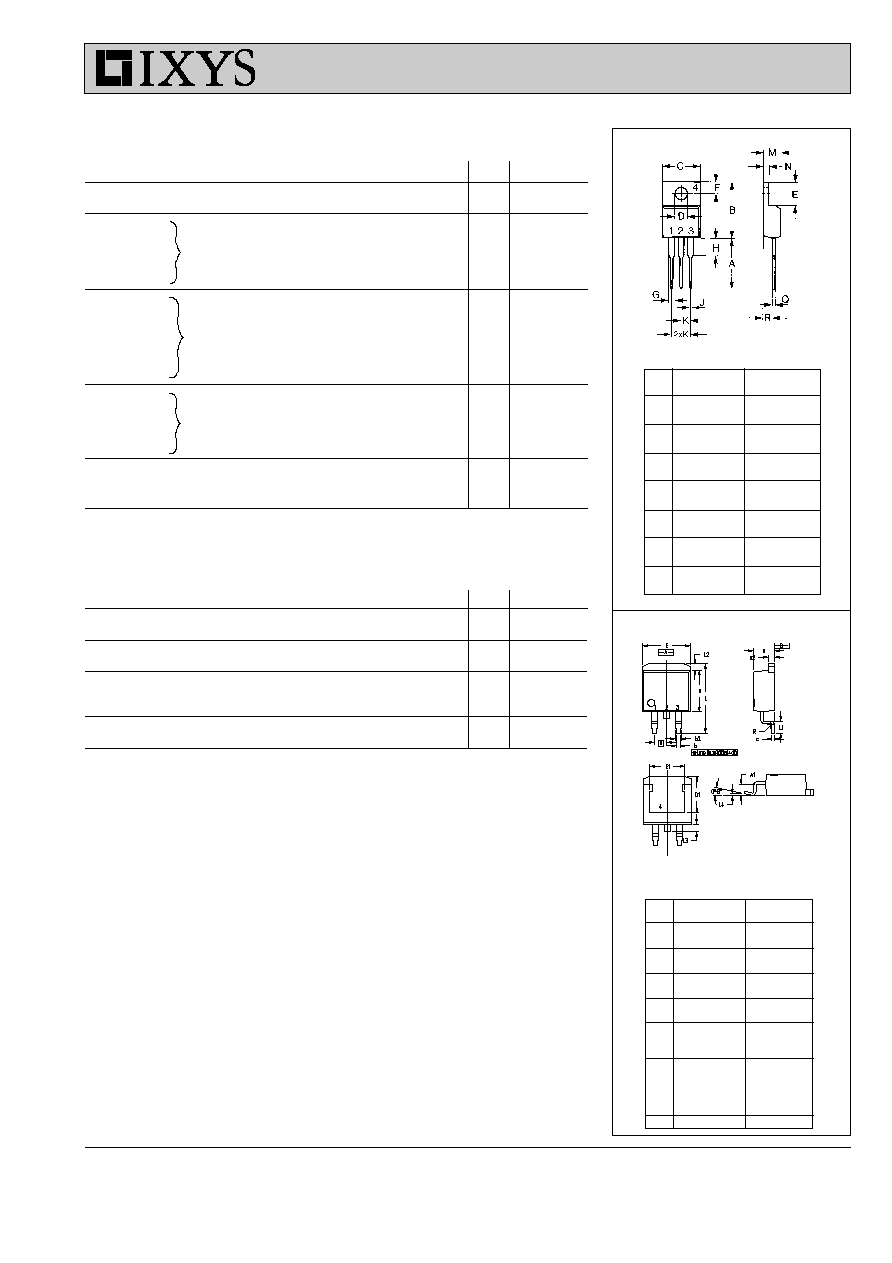
TO-220 AB Outline
Dim.
Millimeter
Inches
Min.
Max.
Min.
Max.
A
12.70
13.97
0.500
0.550
B
14.73
16.00
0.580
0.630
C
9.91
10.66
0.390
0.420
D
3.54
4.08
0.139
0.161
E
5.85
6.85
0.230
0.270
F
2.54
3.18
0.100
0.125
G
1.15
1.65
0.045
0.065
H
2.79
5.84
0.110
0.230
J
0.64
1.01
0.025
0.040
K
2.54
BSC
0.100
BSC
M
4.32
4.82
0.170
0.190
N
1.14
1.39
0.045
0.055
Q
0.35
0.56
0.014
0.022
R
2.29
2.79
0.090
0.110
1. Gate
2. Collector
3. Emitter
4. Collector
Botton Side
Dim.
Millimeter
Inches
Min.
Max.
Min.
Max.
A
4.06
4.83
.160
.190
A1
2.03
2.79
.080
.110
b
0.51
0.99
.020
.039
b2
1.14
1.40
.045
.055
c
0.46
0.74
.018
.029
c2
1.14
1.40
.045
.055
D
8.64
9.65
.340
.380
D1
7.11
8.13
.280
.320
E
9.65
10.29
.380
.405
E1
6.86
8.13
.270
.320
e
2.54
BSC
.100
BSC
L
14.61
15.88
.575
.625
L1
2.29
2.79
.090
.110
L2
1.02
1.40
.040
.055
L3
1.27
1.78
.050
.070
L4
0
0.38
0
.015
R
0.46
0.74
.018
.029
TO-263 SMD Outline
Pins:
1 - Gate
2 - Collector
3 - Emitter
4 - Collector
Bottom Side
IXYS MOSFETS and IGBTs are covered by one or more of the following U.S. patents:
4,835,592
4,881,106
5,017,508
5,049,961
5,187,117
5,486,715
4,850,072
4,931,844
5,034,796
5,063,307
5,237,481
5,381,025
3 - 4
© 2000 IXYS All rights reserved
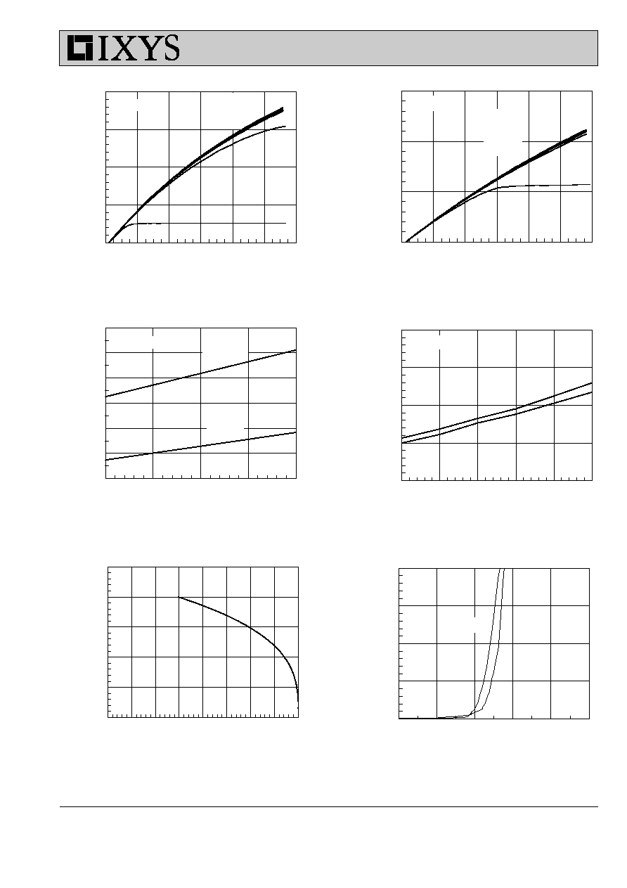
T - Degrees C
-50 -25
0
25
50
75
100 125 150
I
D
-
A
m
p
e
re
s
0.0
0.5
1.0
1.5
2.0
2.5
V
DS
- Volts
0
5
10
15
20
25
30
I
D
- A
m
p
e
re
s
0
1
2
3
V
Volts
0
2
4
6
8
10
I
D
-
A
m
pe
res
0.0
0.5
1.0
1.5
2.0
T
J
- Degrees C
25
50
75
100
125
150
R
DS
(
O
N)
-
No
rm
ali
z
ed
0
1
2
3
4
I
D
= 1 A
I
D
- Amperes
0
1
2
3
4
R
DS
(
O
N
)
-
No
rma
l
i
z
ed
0.5
1.0
1.5
2.0
2.5
3.0
3.5
V
DS
- Volts
0
5
10
15
20
25
30
I
D
-
A
m
pe
res
0
1
2
3
4
5V
V
GS
= 10V
V
GS
=10V
9V
8V
7V
T
J
=125
O
C
V
GS
=10V
T
J
=25
O
C
6V
5V
T
J
= 25
o
C
I
D
= 2 A
T
J
= 25
O
C
T
J
= 125
o
C
V
GS
=10V
9V
8V
7V
6V
T
J
= 125
O
C
Figure 2. Output Characteristics at 125
O
C
Figure 1. Output Characteristics at 25
O
C
Figure 5. Drain Current vs. Case Temperature
Figure 6. Admittance Curves
Figure 3. R
DS(on)
normalized to 0.5 I
D25
value
Figure 4. R
DS(on)
normalized to 0.5 I
D25
value
IXTA2N100
IXTP2N100
4 - 4
© 2000 IXYS All rights reserved
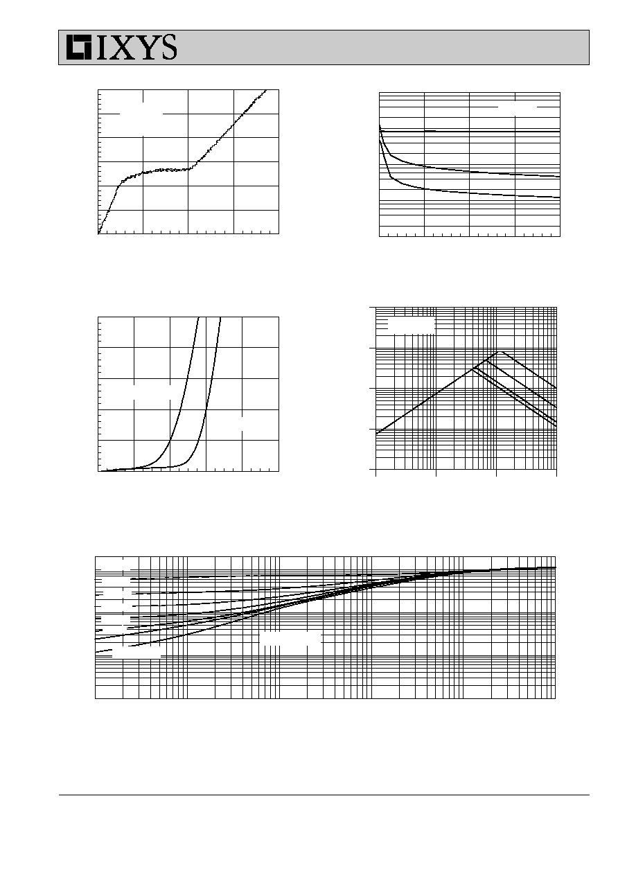
V
DS
- Volts
1
1 0
1 00
1 000
I
D
-
A
m
p
e
re
s
0. 01
0. 1
1
1 0
1 00
V
DS
- Volts
0
10
20
30
40
C
a
pa
citanc
e - pF
1
10
100
1000
10000
V
SD
- Volts
0.2
0.4
0.6
0.8
1.0
1.2
I
D
-
A
m
p
e
re
s
0
1
2
3
4
5
Gate Charge - nC
0
10
20
30
40
V
GS
- V
o
lts
0
2
4
6
8
10
12
Crss
Coss
Ciss
Vds= 500V
I
D
= 1A
I
G
= 1mA
f = 1MHz
2
T
C
= 25
O
C
10 ms
1 ms
100 ms
DC
T
J
= 125
O
C
T
J
= 25
O
C
Pulse Width - Seconds
0.00001
0.0001
0.001
0.01
0.1
1
Z
th
JC
(
K
/W
)
0.001
0.01
0.1
1
D=0.5
D=0.1
D=0.05
D=0.01
Single pulse
D = Duty Cycle
D=0.2
D=0.02
Figure 8. Capacitance Curves
Figure 7. Gate Charge
Figure 9. Source Current vs. Source to Drain Voltage
Figure 11. Transient Thermal Resistance
Figure10. Forward Bias Safe Operating Area
IXTA2N100
IXTP2N100