© 1997 IXYS All rights reserved
G = Gate,
C = Collector,
E = Emitter,
TAB = Collector
Symbol
Test Conditions
Maximum Ratings
V
CES
T
J
= 25
°
C to 150
°
C
600
V
V
CGR
T
J
= 25
°
C to 150
°
C; R
GE
= 1 M
600
V
V
GES
Continuous
±
20
V
V
GEM
Transient
±
30
V
I
C25
T
C
= 25
°
C, limited by leads
75
A
I
C90
T
C
= 90
°
C
50
A
I
CM
T
C
= 25
°
C, 1 ms
200
A
SSOA
V
GE
= 15 V, T
VJ
= 125
°
C, R
G
= 22
I
CM
= 100
A
(RBSOA)
Clamped inductive load, L = 30
µ
H
@ 0.8 V
CES
t
SC
V
GE
= 15 V, V
CE
= 360 V, T
J
= 125
°
C
10
µ
s
(SCSOA)
R
G
= 22
,
non repetitive
P
C
T
C
= 25
°
C
300
W
T
J
-55 ... +150
°
C
T
JM
150
°
C
T
stg
-55 ... +150
°
C
Weight
6
g
Maximum lead temperature for soldering
300
°
C
1.6 mm (0.062 in.) from case for 10 s
V
CES
= 600 V
I
C25
= 75 A
V
CE(sat)
= 2.7 V
Symbol
Test Conditions
Characteristic Values
(T
J
= 25
°
C, unless otherwise specified)
min.
typ.
max.
BV
CES
I
C
= 3 mA, V
GE
= 0 V
600
V
V
GE(th)
I
C
= 4 mA, V
CE
= V
GE
4
8
V
I
CES
V
CE
= 0.8 · V
CES
T
J
= 25
°
C
750
µ
A
V
GE
= 0 V
T
J
= 125
°
C
15
mA
I
GES
V
CE
= 0 V, V
GE
=
±
20 V
±
100
nA
V
CE(sat)
I
C
= I
C90
, V
GE
= 15 V
2.7
V
Features
l
Hole-less TO-247 package for clip
mounting
l
High current rating
l
Guaranteed Short Circuit SOA
capability
l
High frequency IGBT and anti-
parallel FRED in one package
l
Low V
CE(sat)
- for minimum on-state conduction
losses
l
MOS Gate turn-on
- drive simplicity
l
Fast Recovery
Epitaxial Diode (FRED)
- soft recovery with low I
RM
Applications
l
AC motor speed control
l
DC servo and robot drives
l
DC choppers
l
Uninterruptible power supplies (UPS)
l
Switch-mode and resonant-mode
power supplies
Advantages
l
Space savings (two devices in one
package)
l
High power density
97512 (5/97)
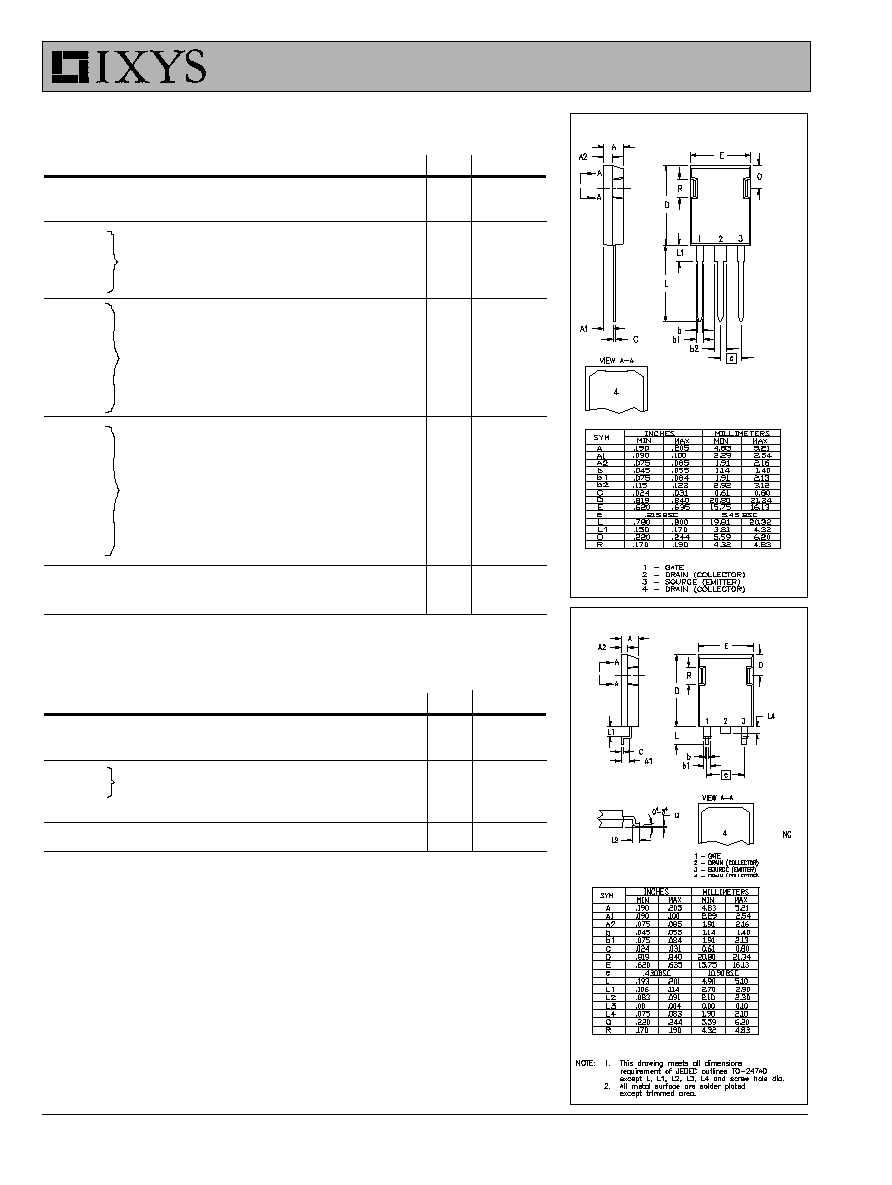
TO-247 Hole-less
(50N60AU1)
G
C
E
C (TAB)
E
G
C (TAB)
TO-247 Hole-less SMD
(50N60AU1S)
IXSX50N60AU1
IXSX50N60AU1S
IGBT with Diode
Combi Pack
Short Circuit SOA Capability
Preliminary data
IXYS MOSFETS and IGBTs are covered by one or more of the following U.S. patents:
4,835,592
4,881,106
5,017,508
5,049,961
5,187,117
5,486,715
4,850,072
4,931,844
5,034,796
5,063,307
5,237,481
5,381,025
IXYS reserves the right to change limits, test conditions, and dimensions.
IXSX50N60AU1
IXSX50N60AU1S
Symbol
Test Conditions
Characteristic Values
(T
J
= 25
°
C, unless otherwise specified)
min.
typ.
max.
g
fs
I
C
= I
C90
; V
CE
= 10 V,
20
23
S
Pulse test, t
300
µ
s, duty cycle
2 %
Q
g
190
250
nC
Q
ge
I
C
= I
C90
, V
GE
= 15 V, V
CE
= 0.5 V
CES
45
60
nC
Q
gc
88
120
nC
t
d(on)
70
ns
t
ri
220
ns
t
d(off)
200
ns
t
fi
400
600
ns
E
off
6
mJ
t
d(on)
70
ns
t
ri
230
ns
E
on
4.5
mJ
t
d(off)
340
ns
t
fi
400
ns
E
off
7
mJ
R
thJC
0.42 K/W
R
thCK
0.15
K/W
Reverse Diode (FRED)
Characteristic Values
(T
J
= 25
°
C, unless otherwise specified)
Symbol
Test Conditions
min.
typ.
max.
V
F
I
F
= I
C90
, V
GE
= 0 V,
1.8
V
Pulse test, t
300
µ
s, duty cycle d
2 %
I
RM
I
F
= I
C90
, V
GE
= 0 V, -di
F
/dt = 480 A/
µ
s
19
33
A
t
rr
V
R
= 360 V
T
J
= 125
°
C
175
ns
I
F
= 1 A; -di/dt = 200 A/
µ
s; V
R
= 30 V T
J
= 25
°
C
35
50
ns
R
thJC
0.75 K/W
Inductive load, T
J
= 25
°°
°°
°
C
I
C
= I
C90
, V
GE
= 15 V, L = 100
µ
H,
V
CE
= 0.8 V
CES
, R
G
= 2.7
Remarks: Switching times may increase
for V
CE
(Clamp) > 0.8 · V
CES
, higher T
J
or
increased R
G
Inductive load, T
J
= 125
°°
°°
°
C
I
C
= I
C90
, V
GE
= 15 V, L = 100
µ
H
V
CE
= 0.8 V
CES
, R
G
= 2.7
Remarks: Switching times may increase
for V
CE
(Clamp) > 0.8 · V
CES
, higher T
J
or
increased R
G
TO-247 HOLE-LESS SMD
TO-247 HOLE-LESS
© 1997 IXYS All rights reserved
T
J
- Degrees C
-50
-25
0
25
50
75
100 125 150
BV
/
V
G
E
(th)
-
N
orma
l
i
z
e
d
0.7
0.8
0.9
1.0
1.1
1.2
1.3
BV
CES
I
C
= 3mA
V
GE
- Volts
4
5
6
7
8
9
10
11
12
13
I
C
- Am
per
es
0
10
20
30
40
50
60
70
80
T
J
- Degrees C
-50
-25
0
25
50
75
100 125 150
V
CE
(
s
a
t
)
-
No
rm
a
liz
ed
0.7
0.8
0.9
1.0
1.1
1.2
1.3
1.4
1.5
V
GE
- Volts
8
9
10
11
12
13
14
15
V
CE
-
Vo
lt
s
0
1
2
3
4
5
6
7
8
9
10
V
CE
- Volts
0
2
4
6
8
10 12 14 16 18 20
I
C
-
Am
p
e
r
e
s
0
20
40
60
80
100
120
140
160
180
200
7V
9V
11V
13V
V
CE
- Volts
0
1
2
3
4
5
I
C
-
Am
p
e
r
e
s
0
10
20
30
40
50
60
70
80
11V
7V
9V
13V
T
J
= 25°C
V
GE
= 15V
T
J
= 25°C
V
GE
= 15V
T
J
= 25°C
I
C
= 20A
I
C
= 40A
I
C
= 80A
I
C
= 20A
I
C
= 40A
I
C
= 80A
V
GE
=15V
V
CE
= 10V
T
J
= 125°C
T
J
= 25°C
T
J
= - 40°C
V
GE8th)
I
C
= 4mA
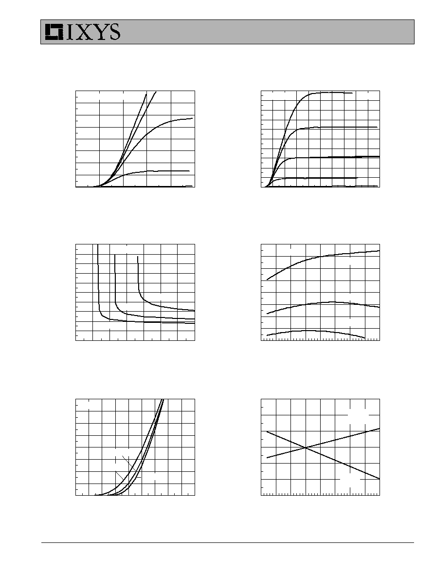
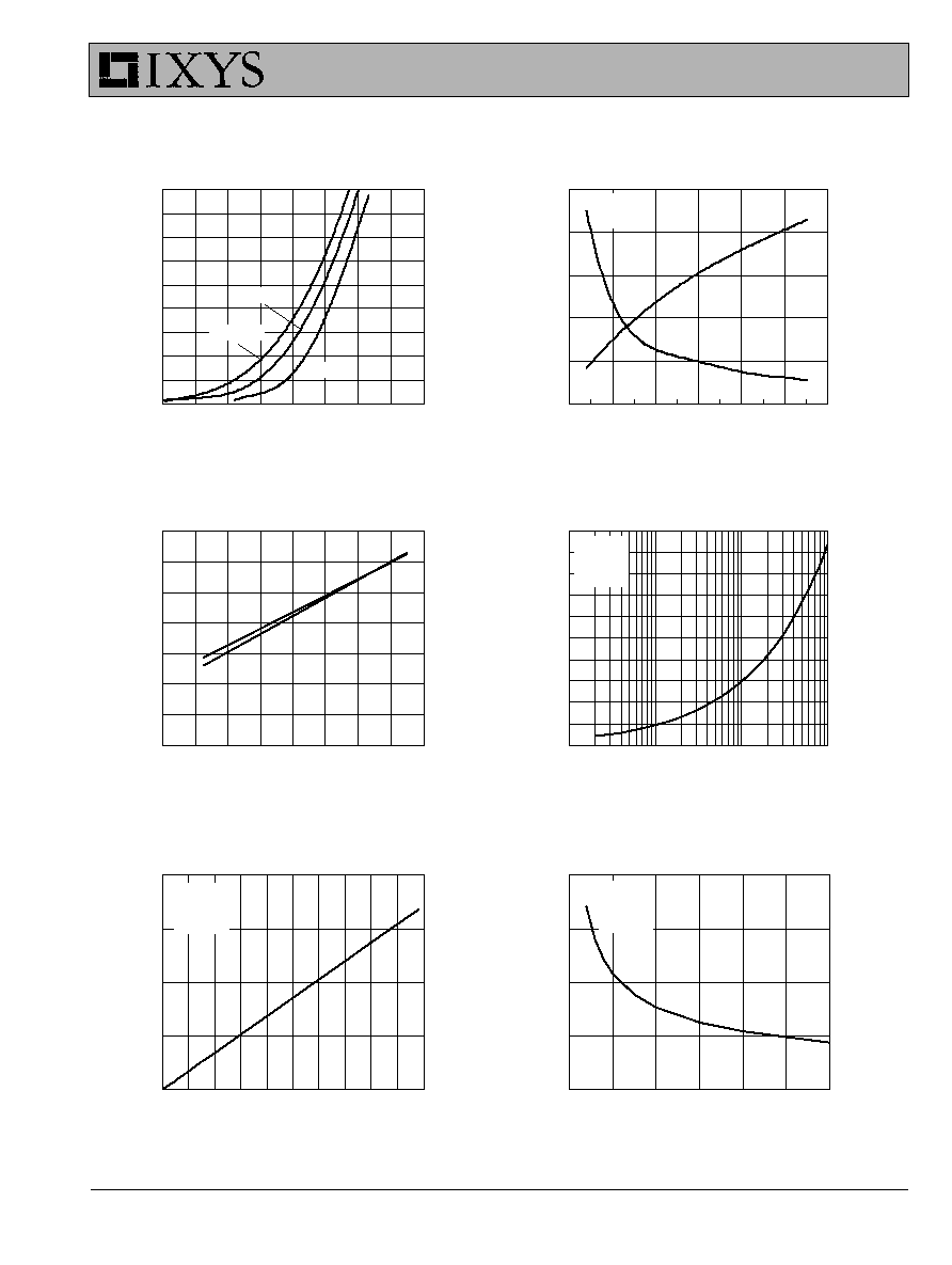
Fig. 3 Collector-Emitter Voltage
Fig. 4
Temperature Dependence
vs. Gate-Emitter Voltage
of Output Saturation Voltage
Fig.5 Input Admittance
Fig.6
Temperature Dependence of
Breakdown and Threshold Voltage
Fig.1 Saturation Characteristics
Fig.2 Output Characterstics
IXSX50N60AU1
IXSX50N60AU1S
IXYS MOSFETS and IGBTs are covered by one or more of the following U.S. patents:
4,835,592
4,881,106
5,017,508
5,049,961
5,187,117
5,486,715
4,850,072
4,931,844
5,034,796
5,063,307
5,237,481
5,381,025
IXYS reserves the right to change limits, test conditions, and dimensions.
IXSX50N60AU1
IXSX50N60AU1S
V
CE
- Volts
0
100
200
300
400
500
600
700
I
C
-
Am
pe
res
0.01
0.1
1
10
100
1000
T
J
= 125°C
R
G
= 22
dV/dt < 6V/ns
Q
g
- nCoulombs
0
50
100
150
200
250
V
GE
- V
olts
0
3
6
9
12
15
R
G
- Ohms
0
10
20
30
40
50
E
of
f
-
m
illijo
ule
s
0
2
4
6
8
10
t
fi
- na
no
sec
on
ds
0
200
400
600
800
1000
I
C
- Amperes
0
10
20
30
40
50
60
70
80
t
fi
- na
no
sec
on
ds
0
250
500
750
1000
E
of
f
- m
illij
oul
es
0
3
6
9
12
Time - Seconds
0.00001
0.0001
0.001
0.01
0.1
1
Th
erm
al
Res
po
nse
- K
/
W
0.001
0.01
0.1
1
I
C
= 50A
V
CE
= 480V
t
fi
E
off
T
J
= 125°C
R
G
= 10
t
fi
E
off
T
J
= 125°C
I
C
= 50A
IGBT
Diode
Single Pulse
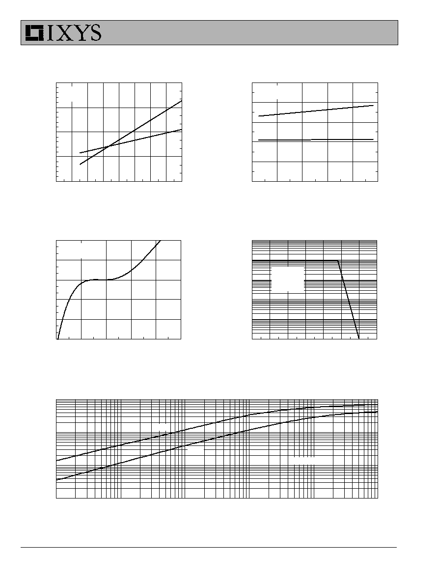
Fig.11 Transient Thermal Impedance
Fig.9 Gate Charge Characteristic Curve
Fig.10 Turn-Off Safe Operating Area
Fig.7 Turn-Off Energy per Pulse and
Fig.8 Dependence of Turn-Off Energy
Fall Time on Collector Current
Per Pulse and Fall Time on R
G
© 1997 IXYS All rights reserved
di
F
/dt - A/µs
0
200
400
600
t
rr
- n
a
n
o
s
eco
nd
s
0
200
400
600
800
di
F
/dt - A/µs
200
400
600
800
1000
I
RM
-
Am
pe
res
0
20
40
60
80
max
di
F
/dt - A/µs
1
10
100
1000
Q
r
-
na
noc
ou
lom
bs
0
1
2
3
4
5
T
J
- Degrees C
0
40
80
120
160
Nor
ma
lize
d I
RM
/ Q
r
0.0
0.2
0.4
0.6
0.8
1.0
1.2
1.4
Q
r
I
RM
di
F
/dt - A/µs
0
200
400
600
800
1000
1200
t
fr
- n
a
n
ose
co
nd
s
0
200
400
600
800
1000
V
FR
- Vo
lts
0
4
8
12
16
20
t
fr
V
FR
Voltage Drop - Volts
0.5
1.0
1.5
2.0
2.5
C
u
r
ren
t -
Am
pe
res
0
20
40
60
80
100
120
140
160
180
T
J
= 100°C
V
R
= 350V
I
F
= 60A
T
J
= 125°C
I
F
= 60A
T
J
= 100°C
T
J
= 150°C
T
J
= 25°C
T
J
= 100°C
V
R
= 350V
I
F
= 60A
T
J
= 100°C
V
R
= 350V
I
F
= 60A
Fig.14 Junction Temperature Dependence
Fig.15 Reverse Recovery Chargee
off I
RM
and Q
r
Fig.16 Peak Reverse Recovery Current
Fig.17 Reverse Recovery Time
Fig.12 Typical Forward Voltage Drop
Fig.13
Peak Forward Voltage V
FR
and
Forward Recovery Time t
fr
IXSX50N60AU1
IXSX50N60AU1S