ę 1996 IXYS All rights reserved
Symbol
Test Conditions
Maximum Ratings
V
CES
T
J
= 25
░
C to 150
░
C
600
V
V
CGR
T
J
= 25
░
C to 150
░
C; R
GE
= 1 M
600
V
V
GES
Continuous
▒
20
V
V
GEM
Transient
▒
30
V
I
C25
T
C
= 25
░
C
20
A
I
C90
T
C
= 90
░
C
10
A
I
CM
T
C
= 25
░
C, 1 ms
40
A
SSOA
V
GE
= 15 V, T
J
= 125
░
C, R
G
= 150
I
CM
= 20
A
(RBSOA)
Clamped inductive load, L = 300
Á
H
@ 0.8 V
CES
t
SC
V
GE
= 15 V, V
CE
= 360 V, T
J
= 125
░
C
10
Á
s
(SCSOA)
R
G
= 82
,
non repetitive
P
C
T
C
= 25
░
C
100
W
T
J
-55 ... +150
░
C
T
JM
150
░
C
T
stg
-55 ... +150
░
C
M
d
Mounting torque
1.13/10 Nm/lb.in.
Weight
6 g
Maximum lead temperature for soldering
300
░
C
1.6 mm (0.062 in.) from case for 10 s
Features
Ě
International standard packages
Ě
Guaranteed Short Circuit SOA
capability
Ě
Low V
CE(sat)
- for low on-state conduction losses
Ě
High current handling capability
Ě
MOS Gate turn-on
- drive simplicity
Ě
Fast Fall Time for switching speeds
up to 20 kHz
Applications
Ě
AC motor speed control
Ě
Uninterruptible power supplies (UPS)
Ě
Welding
Advantages
Ě
Easy to mount with 1 screw
(isolated mounting screw hole)
Ě
High power density
Preliminary data
High Speed IGBT
Short Circuit SOA Capability
95562B(10/96)
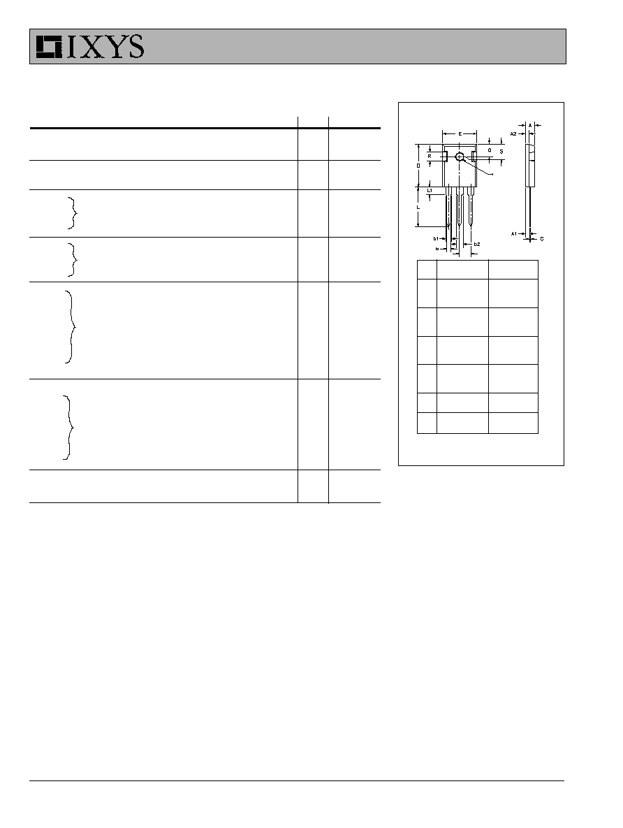
C (TAB)
G
C
E
TO-247 AD
G = Gate
C = Collector
E = Emitter
Tab = Collector
Symbol
Test Conditions
Characteristic Values
(T
J
= 25
░
C, unless otherwise specified)
min.
typ.
max.
BV
CES
I
C
= 250
Á
A, V
GE
= 0 V
600
V
V
GE(th)
I
C
= 750
Á
A, V
CE
= V
GE
3.5
6.5
V
I
CES
V
CE
= 0.8 Ě V
CES
T
J
= 25
░
C
200
Á
A
V
GE
= 0 V
T
J
= 125
░
C
1
mA
I
GES
V
CE
= 0 V, V
GE
=
▒
20 V
▒
100
nA
V
CE(sat)
I
C
= I
C90
, V
GE
= 15 V
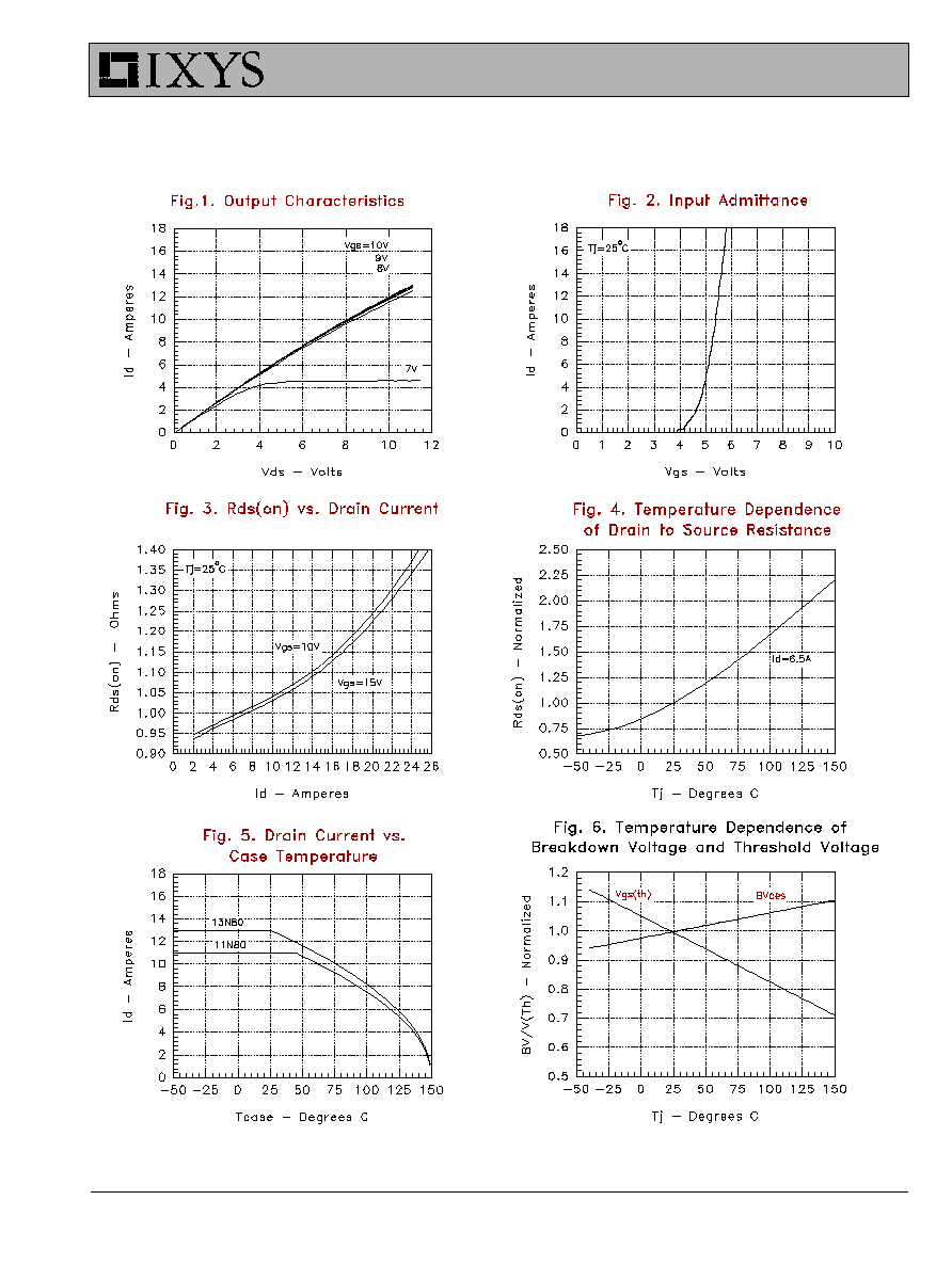
10N60
2.5
V
10N60A
3.0
V
V
CES
I
C(25)
V
CE(sat)
600 V
20 A
2.5 V
600 V
20 A
3.0 V
IXSH10N60
IXSH10N60A
IXYS MOSFETS and IGBTs are covered by one or more of the following U.S. patents:
4,835,592
4,881,106
5,017,508
5,049,961
5,187,117
5,486,715
4,850,072
4,931,844
5,034,796
5,063,307
5,237,481
5,381,025
IXYS reserves the right to change limits, test conditions, and dimensions.
IXSH10N60
IXSH10N60A
Dim.
Millimeter
Inches
Min.
Max.
Min.
Max.
A
4.7
5.3
.185
.209
A
1
2.2
2.54
.087
.102
A
2
2.2
2.6
.059
.098
b
1.0
1.4
.040
.055
b
1
1.65
2.13
.065
.084
b
2
2.87
3.12
.113
.123
C
.4
.8
.016
.031
D
20.80
21.46
.819
.845
E
15.75
16.26
.610
.640
e
5.20
5.72
0.205 0.225
L
19.81
20.32
.780
.800
L1
4.50
.177
P
3.55
3.65
.140
.144
Q
5.89
6.40
0.232 0.252
R
4.32
5.49
.170
.216
S
6.15 BSC
242 BSC
e
P
TO-247 AD Outline
Symbol
Test Conditions
Characteristic Values
(T
J
= 25
░
C, unless otherwise specified)
min.
typ. max.
g
fs
I
C
= I
C90
; V
CE
= 10 V,
2
S
Pulse test, t
300
Á
s, duty cycle
2 %
I
C(on)
V
GE
= 15 V, V
CE
= 10 V
50
A
C
ies
750
pF
C
oes
V
CE
= 25 V, V
GE
= 0 V, f = 1 MHz
125
pF
C
res
30
pF
Q
g
40
nC
Q
ge
I
C
= I
C90
, V
GE
= 15 V, V
CE
= 0.5 V
CES
12
nC
Q
gc
20
80
nC
t
d(on)
100
ns
t
ri
200
ns
t
d(off)
250
750
ns
t
fi
10N60A
175
410
n s
10N60
720
ns
E
off
10N60A
0.75
1.2
mJ
Note 1
10N60
1.2
1.9
mJ
t
d(on)
100
ns
t
ri
200
ns
E
on
1.0
mJ
t
d(off)
300
ns
t
fi
10N60AU1
400
ns
E
off
Note 1
10N60AU1
1.5
mJ
R
thJC
1.25
K/W
R
thCK
0.25
K/W
Inductive load, T
J
= 25
░░
░░
░
C
I
C
= I
C90
, V
GE
= 15 V,
L = 300
Á
H, V
CE
= 0.8 V
CES
,
R
G
= 150
Notes:
1.
Switching times may increase for V
CE
(Clamp) > 0.8 Ě V
CES
, higher T
J
or R
G
values.
2.
Device must be heatsunk for high temperature leakage current
measurements to avoid thermal runaway.
Inductive load, T
J
= 125
░░
░░
░
C
I
C
= I
C90
, V
GE
= 15 V,
L = 300
Á
H, V
CE
= 0.8 V
CES
,
R
G
= 150
IXYS MOSFETS and IGBTs are covered by one or more of the following U.S. patents:
4,835,592
4,881,106
5,017,508
5,049,961
5,187,117
5,486,715
4,850,072
4,931,844
5,034,796
5,063,307
5,237,481
5,381,025
IXYS reserves the right to change limits, test conditions, and dimensions.
IXSH10N60
IXSH10N60A