
© 1996 IXYS All rights reserved
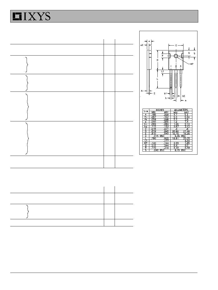
TO-247 AD
G
C
E
G = Gate,
C = Collector,
E = Emitter,
TAB = Collector
Symbol
Test Conditions
Maximum Ratings
V
CES
T
J
= 25
°
C to 150
°
C
600
V
V
CGR
T
J
= 25
°
C to 150
°
C; R
GE
= 1 M
600
V
V
GES
Continuous
±
20
V
V
GEM
Transient
±
30
V
I
C25
T
C
= 25
°
C
76
A
I
C90
T
C
= 90
°
C
38
A
I
CM
T
C
= 25
°
C, 1 ms
152
A
SSOA
V
GE
= 15 V, T
VJ
= 125
°
C, R
G
= 10
I
CM
= 76
A
(RBSOA)
Clamped inductive load, L = 100
µ
H
@ 0.8 V
CES
P
C
T
C
= 25
°
C
200
W
T
J
-55 ... +150
°
C
T
JM
150
°
C
T
stg
-55 ... +150
°
C
M
d
Mounting torque (M3)
1.13/10 Nm/lb.in.
Weight
6
g
Maximum lead temperature for soldering
300
°
C
1.6 mm (0.062 in.) from case for 10 s
Symbol
Test Conditions
Characteristic Values
(T
J
= 25
°
C, unless otherwise specified)
min.
typ.
max.
BV
CES
I
C
= 750
µ
A, V
GE
= 0 V
600
V
V
GE(th)
I
C
= 250
µ
A, V
CE
= V
GE
2.5
5.5
V
I
CES
V
CE
= 0.8 · V
CES
T
J
= 25
°
C
500
µ
A
V
GE
= 0 V
T
J
= 125
°
C
8
mA
I
GES
V
CE
= 0 V, V
GE
=
±
20 V
±
100
nA
V
CE(sat)
I
C
= I
C90
, V
GE
= 15 V
1.8
V
Ultra-Low V
CE(sat)
IXGH 38N60U1
V
CES
= 600 V
IGBT with Diode
I
C25
= 76 A
V
CE(sat)
= 1.8 V
Combi Pack
Features
l
International standard package
JEDEC TO-247 AD
l
IGBT and anti-parallel FRED in one
package
l
2nd generation HDMOS
TM
process
l
Low V
CE(sat)
- for minimum on-state conduction
losses
l
MOS Gate turn-on
- drive simplicity
l
Fast Recovery
Epitaxial Diode (FRED)
- soft recovery with low I
RM
Applications
l
AC motor speed control
l
DC servo and robot drives
l
DC choppers
l
Uninterruptible power supplies (UPS)
l
Switch-mode and resonant-mode
power supplies
Advantages
l
Space savings (two devices in one
package)
l
Easy to mount with 1 screw
(isolated mounting screw hole)
l
Reduces assembly time and cost
l
High power density
94528B (3/96)
IXYS MOSFETS and IGBTs are covered by one or more of the following U.S. patents:
4,835,592
4,881,106
5,017,508
5,049,961
5,187,117
5,486,715
4,850,072
4,931,844
5,034,796
5,063,307
5,237,481
5,381,025
IXYS reserves the right to change limits, test conditions, and dimensions.
IXGH 38N60U1
Symbol
Test Conditions
Characteristic Values
(T
J
= 25
°
C, unless otherwise specified)
min.
typ.
max.
g
fs
I
C
= I
C90
; V
CE
= 10 V,
15
20
S
Pulse test, t
300
µ
s, duty cycle
2 %
C
ies
2500
pF
C
oes
V
CE
= 25 V, V
GE
= 0 V, f = 1 MHz
270
pF
C
res
70
pF
Q
g
125
150
nC
Q
ge
I
C
= I
C90
, V
GE
= 15 V, V
CE
= 0.5 V
CES
23
35
nC
Q
gc
50
75
nC
t
d(on)
30
ns
t
ri
150
ns
t
d(off)
600
1200
ns
t
fi
500
700
ns
E
off
9
15
mJ
t
d(on)
40
ns
t
ri
160
ns
E
on
1
mJ
t
d(off)
800
ns
t
fi
1000
ns
E
off
15
mJ
R
thJC
0.62 K/W
R
thCK
0.25
K/W
Reverse Diode (FRED)
Characteristic Values
(T
J
= 25
°
C, unless otherwise specified)
Symbol
Test Conditions
min.
typ.
max.
V
F
I
F
= I
C90
, V
GE
= 0 V,
1.6
V
Pulse test, t
300
µ
s, duty cycle d
2 %
I
RM
I
F
= I
C90
, V
GE
= 0 V, -di
F
/dt = 240 A/
µ
s
10
15
A
t
rr
V
R
= 360 V
T
J
= 125
°
C
150
ns
I
F
= 1 A; -di/dt = 100 A/
µ
s; V
R
= 30 V T
J
= 25
°
C
35
50
ns
R
thJC
1 K/W
TO-247 AD Outline
Inductive load, T
J
= 25
°°
°°
°
C
I
C
= I
C90
, V
GE
= 15 V, L = 100
µ
H,
V
CE
= 0.8 V
CES
, R
G
= R
off
= 10
Remarks: Switching times may increase
for V
CE
(Clamp) > 0.8 · V
CES
, higher T
J
or
increased R
G
1 = Gate
2 = Collector
3 = Emitter
Tab = Collector
Inductive load, T
J
= 125
°°
°°
°
C
I
C
= I
C90
, V
GE
= 15 V, L = 100
µ
H
V
CE
= 0.8 V
CES
, R
G
= R
off
= 10
Remarks: Switching times may increase
for V
CE
(Clamp) > 0.8 · V
CES
, higher T
J
or
increased R
G