© 1996 IXYS All rights reserved
Symbol
Test Conditions
Maximum Ratings
V
CES
T
J
= 25
°
C to 150
°
C
1000
V
V
CGR
T
J
= 25
°
C to 150
°
C; R
GE
= 1 M
1000
V
V
GES
Continuous
±
20
V
V
GEM
Transient
±
30
V
I
C25
T
C
= 25
°
C
50
A
I
C90
T
C
= 90
°
C
25
A
I
CM
T
C
= 25
°
C, 1 ms
100
A
SSOA
V
GE
= 15 V, T
VJ
= 125
°
C, R
G
= 33
I
CM
= 50
A
(RBSOA)
Clamped inductive load, L = 100
µ
H
@ 0.8 V
CES
P
C
T
C
= 25
°
C
200
W
T
J
-55 ... +150
°
C
T
JM
150
°
C
T
stg
-55 ... +150
°
C
M
d
Mounting torque (M3)
1.13/10 Nm/lb.in.
Weight
TO-204 = 18 g, TO-247 = 6 g
Maximum lead temperature for soldering
300
°
C
1.6 mm (0.062 in.) from case for 10 s
Symbol
Test Conditions
Characteristic Values
(T
J
= 25
°
C, unless otherwise specified)
min.
typ.
max.
BV
CES
I
C
= 3 mA, V
GE
= 0 V
1000
V
V
GE(th)
I
C
= 250
µ
A, V
CE
= V
GE
2.5
5
V
I
CES
V
CE
= 0.8 · V
CES
T
J
= 25
°
C
250
µ
A
V
GE
= 0 V
T
J
= 125
°
C
1
mA
I
GES
V
CE
= 0 V, V
GE
=
±
20 V
±
100
nA
V
CE(sat)
I
C
= I
C90
, V
GE
= 15 V
25N100
3.5
V
25N100A
4.0
V
TO-247 AD (IXGH)
G
C
E
TO-204 AE (IXGM)
C
G = Gate,
C = Collector,
E = Emitter,
TAB = Collector
V
CES
I
C25
V
CE(sat)
Low V
CE(sat)
IXGH/IXGM
25
N100
1000 V
50 A
3.5 V
High speed IGBT
IXGH/IXGM
25
N100A 1000 V
50 A
4.0 V
Features
l
International standard packages
l
2nd generation HDMOS
TM
process
l
Low V
CE(sat)
- for low on-state conduction losses
l
High current handling capability
l
MOS Gate turn-on
- drive simplicity
l
Voltage rating guaranteed at high
temperature (125
°
C)
Applications
l
AC motor speed control
l
DC servo and robot drives
l
DC choppers
l
Uninterruptible power supplies (UPS)
l
Switch-mode and resonant-mode
power supplies
Advantages
l
Easy to mount with 1 screw (TO-247)
(isolated mounting screw hole)
l
High power density
91516E (3/96)
IXYS MOSFETS and IGBTs are covered by one or more of the following U.S. patents:
4,835,592
4,881,106
5,017,508
5,049,961
5,187,117
5,486,715
4,850,072
4,931,844
5,034,796
5,063,307
5,237,481
5,381,025
IXYS reserves the right to change limits, test conditions, and dimensions.
IXGH 25N100
IXGM 25N100
IXGH 25N100A
IXGM 25N100A
Symbol
Test Conditions
Characteristic Values
(T
J
= 25
°
C, unless otherwise specified)
min.
typ.
max.
g
fs
I
C
= I
C90
; V
CE
= 10 V,
8
15
S
Pulse test, t
300
µ
s, duty cycle
2 %
C
ies
2750
pF
C
oes
V
CE
= 25 V, V
GE
= 0 V, f = 1 MHz
200
pF
C
res
50
pF
Q
g
130
180
nC
Q
ge
I
C
= I
C90
, V
GE
= 15 V, V
CE
= 0.5 V
CES
25
60
nC
Q
gc
55
90
nC
t
d(on)
100
ns
t
ri
200
ns
t
d(off)
500
ns
t
fi
25N100A
500
ns
E
off
25N100A
5
mJ
t
d(on)
100
ns
t
ri
250
ns
E
on
3.5
mJ
t
d(off)
720
1000
ns
t
fi
25N100
950
3000
ns
25N100A
800
1500
ns
E
off
25N100
10
mJ
25N100A
8
mJ
R
thJC
0.62 K/W
R
thCK
0.25
K/W
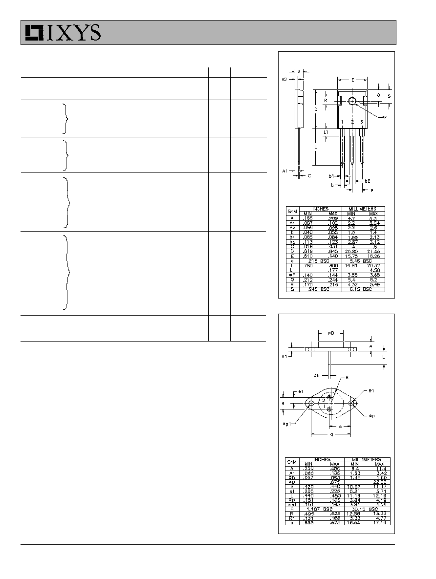
TO-247 AD Outline
TO-204AE Outline
Inductive load, T
J
= 25
°°
°°
°
C
I
C
= I
C90
, V
GE
= 15 V, L = 300
µ
H,
V
CE
= 0.8 V
CES
, R
G
= R
off
= 33
Remarks: Switching times
may increase
for V
CE
(Clamp) > 0.8 · V
CES
,
higher T
J
or increased R
G
1 = Gate
2 = Emitter
Case = Collector
1 = Gate
2 = Collector
3 = Emitter
Tab = Collector
Inductive load, T
J
= 125
°°
°°
°
C
I
C
= I
C90
, V
GE
= 15 V, L = 300
µ
H
V
CE
= 0.8 V
CES
, R
G
= R
off
= 33
Remarks: Switching times
may increase
for V
CE
(Clamp) > 0.8 · V
CES
,
higher T
J
or increased R
G
© 1996 IXYS All rights reserved
T
J
- Degrees C
-50
-25
0
25
50
75
100 125 150
BV
/ V
(t
h
)
-
No
rm
aliz
ed
0.6
0.7
0.8
0.9
1.0
1.1
1.2
T
J
- Degrees C
-50
-25
0
25
50
75
100 125 150
V
C
E
(sa
t
)
-
No
rma
lize
d
0.7
0.8
0.9
1.0
1.1
1.2
1.3
1.4
1.5
V
CE
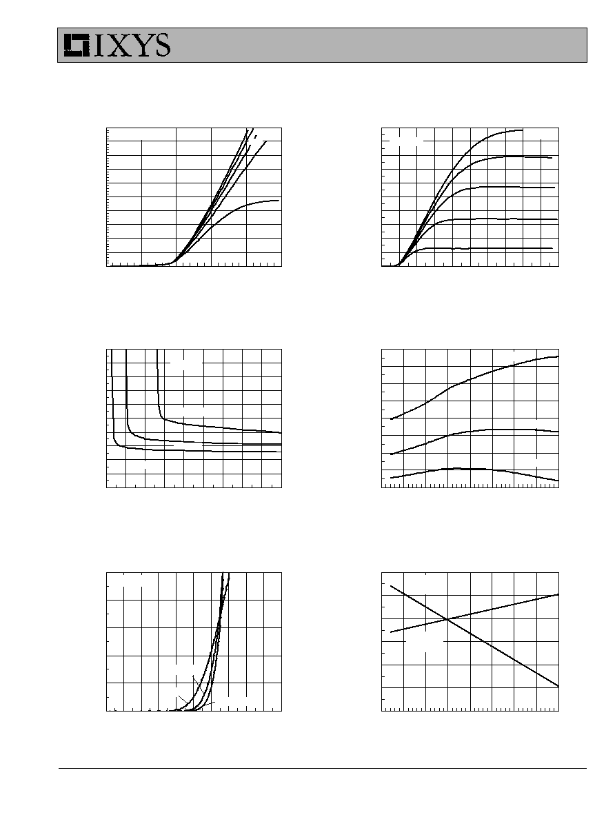
- Volts
0
1
2
3
4
5
I
C
- Am
pe
res
0
5
10
15
20
25
30
35
40
45
50
V
G E
= 15V
7V
9V
V
GE
- Volts
6
7
8
9
10
11
12
13
14
15
V
CE
-
Vo
lts
0
1
2
3
4
5
6
7
8
9
10
V
GE
- Volts
0
1
2
3
4
5
6
7
8
9
10
I
C
- A
m
p
ere
s
0
10
20
30
40
50
V
CE
- Volts
0
2
4
6
8
10
12
14
16
18
20
I
C
-
Am
pe
res
0
20
40
60
80
100
120
140
160
180
200
9V
7V
11V
13V
T
J
= 25°C
T
J
= 25°C
V
GE
= 15V
I
C
= 12.5A
I
C
= 25A
I
C
= 50A
I
C
= 12.5A
I
C
= 25A
I
C
= 50A
T
J
=
- 40°C
T
J
= 125°C
T
J
= 25°C
V
CE
= 10V
13V
11V
T
J
= 25°C
V
GE(th)
I
C
= 250µA
BV
CES
I
C
= 250µA
25N100g1.JNB
Fig. 3 Collector-Emitter Voltage
Fig. 4 Temperature Dependence
vs. Gate-Emitter Voltage
of Output Saturation Voltage
Fig. 5 Input Admittance
Fig. 6 Temperature Dependence of
Breakdown and Threshold Voltage
Fig. 1 Saturation Characteristics
Fig. 2 Output Characterstics
IXGH 25N100
IXGM 25N100
IXGH 25N100A
IXGM 25N100A
IXYS MOSFETS and IGBTs are covered by one or more of the following U.S. patents:
4,835,592
4,881,106
5,017,508
5,049,961
5,187,117
5,486,715
4,850,072
4,931,844
5,034,796
5,063,307
5,237,481
5,381,025
IXYS reserves the right to change limits, test conditions, and dimensions.
IXGH 25N100
IXGM 25N100
IXGH 25N100A
IXGM 25N100A
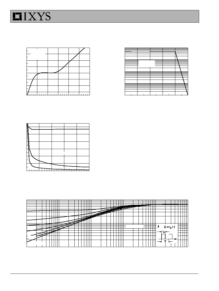
V
CE
- Volts
0
5
10
15
20
25
C
apac
i
t
anc
e -
pF
0
400
800
1200
1600
2000
2400
C
res
Gate Charge - nCoulombs
0
25
50
75
100
125
150
V
GE
- V
o
l
t
s
1
3
5
7
9
11
13
15
V
CE
- Volts
0
200
400
600
800
1000
I
C
-
A
m
per
es
0.01
0.1
1
10
100
Pulse Width - Seconds
0.0001
0.001
0.01
0.1
1
10
Z
th
j
c
(K
/W
)
0.01
0.1
1
Single Pulse
D=0.2
D=0.5
D = Duty Cycle
V
CE
= 800V
I
C
= 25A
I
G
= 10mA
T
J
= 125°C
dV/dt < 3V/ns
C
oes
C
ies
f = 1MHz
D=0.1
D=0.05
D=0.02
D=0.01
25N100g2.JNB
Fig.10 Transient Thermal Impedance
Fig.9 Capacitance Curves
Fig.7 Gate Charge
Fig.8 Turn-Off Safe Operating Area