© 1996 IXYS All rights reserved
Symbol
Test Conditions
Maximum Ratings
V
CES
T
J
= 25
°
C to 150
°
C
1000
V
V
CGR
T
J
= 25
°
C to 150
°
C; R
GE
= 1 M
1000
V
V
GES
Continuous
±
20
V
V
GEM
Transient
±
30
V
I
C25
T
C
= 25
°
C
34
A
I
C90
T
C
= 90
°
C
17
A
I
CM
T
C
= 25
°
C, 1 ms
68
A
SSOA
V
GE
= 15 V, T
VJ
= 125
°
C, R
G
= 82
I
CM
= 34
A
(RBSOA)
Clamped inductive load, L = 300
µ
H
@ 0.8 V
CES
P
C
T
C
= 25
°
C
150
W
T
J
-55 ... +150
°
C
T
JM
150
°
C
T
stg
-55 ... +150
°
C
M
d
Mounting torque (M3)
1.13/10 Nm/lb.in.
Weight
TO-204 = 18 g, TO-247 = 6 g
Maximum lead temperature for soldering
300
°
C
1.6 mm (0.062 in.) from case for 10 s
Symbol
Test Conditions
Characteristic Values
(T
J
= 25
°
C, unless otherwise specified)
min.
typ.
max.
BV
CES
I
C
= 3 mA, V
GE
= 0 V
1000
V
V
GE(th)
I
C
= 250
µ
A, V
CE
= V
GE
2.5
5
V
I
CES
V
CE
= 0.8 · V
CES
T
J
= 25
°
C
250
µ
A
V
GE
= 0 V
T
J
= 125
°
C
1
mA
I
GES
V
CE
= 0 V, V
GE
=
±
20 V
±
100
nA
V
CE(sat)
I
C
= I
C90
, V
GE
= 15 V
17N100
3.5
V
17N100A
4.0
V
TO-247 AD (IXGH)
V
CES
I
C25
V
CE(sat)
Low V
CE(sat)
IGBT
IXGH/IXGM
17
N100
1000 V
34 A
3.5 V
High speed IGBT
IXGH/IXGM
17
N100A 1000 V
34 A
4.0 V
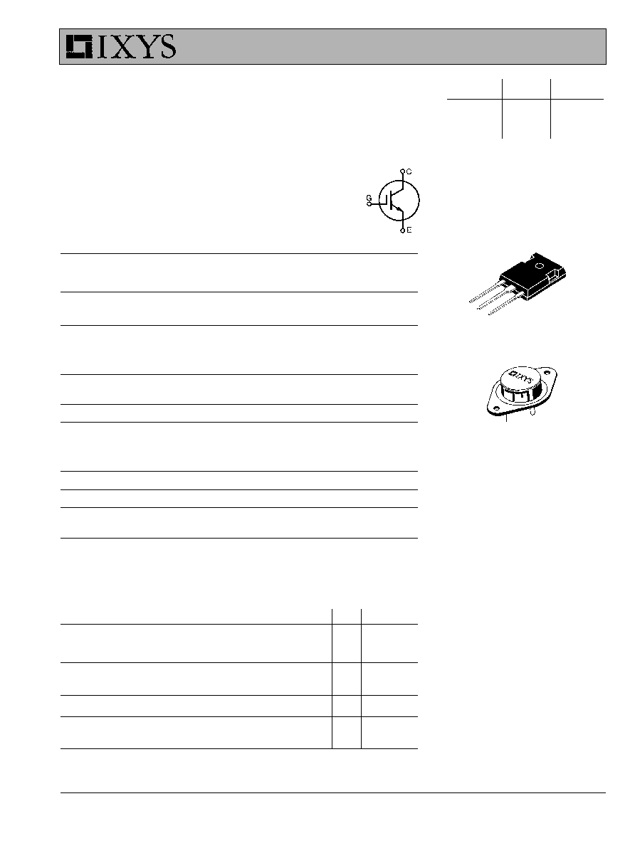
G
C
E
TO-204 AE (IXGM)
C
G = Gate,
C = Collector,
E = Emitter,
TAB = Collector
Features
l
International standard packages
l
2nd generation HDMOS
TM
process
l
Low V
CE(sat)
- for low on-state conduction losses
l
High current handling capability
l
MOS Gate turn-on
- drive simplicity
l
Voltage rating guaranteed at high
temperature (125
°
C)
Applications
l
AC motor speed control
l
DC servo and robot drives
l
DC choppers
l
Uninterruptible power supplies (UPS)
l
Switch-mode and resonant-mode
power supplies
Advantages
l
Easy to mount with 1 screw (TO-247)
(isolated mounting screw hole)
l
High power density
91515E (3/96)
IXYS MOSFETS and IGBTs are covered by one or more of the following U.S. patents:
4,835,592
4,881,106
5,017,508
5,049,961
5,187,117
5,486,715
4,850,072
4,931,844
5,034,796
5,063,307
5,237,481
5,381,025
IXYS reserves the right to change limits, test conditions, and dimensions.
IXGH 17N100
IXGM 17N100
IXGH 17N100A
IXGM 17N100A
Symbol
Test Conditions
Characteristic Values
(T
J
= 25
°
C, unless otherwise specified)
min.
typ.
max.
g
fs
I
C
= I
C90
; V
CE
= 10 V,
6
15
S
Pulse test, t
300
µ
s, duty cycle
2 %
C
ies
1500
pF
C
oes
V
CE
= 25 V, V
GE
= 0 V, f = 1 MHz
175
pF
C
res
40
pF
Q
g
100
120
nC
Q
ge
I
C
= I
C90
, V
GE
= 15 V, V
CE
= 0.5 V
CES
20
30
nC
Q
gc
60
90
nC
t
d(on)
100
ns
t
ri
200
ns
t
d(off)
500
1000
ns
t
fi
17N100
750
ns
17N100A
450
750
ns
E
off
17N100A
3
mJ
t
d(on)
100
ns
t
ri
200
ns
E
on
2.5
mJ
t
d(off)
700
1000
ns
t
fi
17N100
1200
2000
ns
17N100A
750
1000
ns
E
off
17N100
8
mJ
17N100A
6
mJ
R
thJC
0.83 K/W
R
thCK
0.25
K/W
IXGH 17N100 and IXGH 17N100 A characteristic curves are located on the
IXGH 17N100U1 and IXGH 17N100AU1 data sheets.
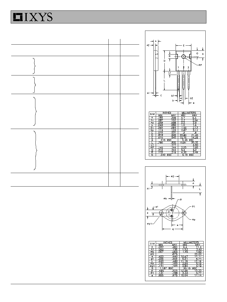
TO-247 AD Outline
Inductive load, T
J
= 25
°°
°°
°
C
I
C
= I
C90
, V
GE
= 15 V, L = 300
µ
H,
V
CE
= 0.8 V
CES
, R
G
= R
off
= 82
Remarks: Switching times
may increase
for V
CE
(Clamp) > 0.8 · V
CES
,
higher T
J
or increased R
G
TO-204AE Outline
1 = Gate
2 = Collector
3 = Emitter
Tab = Collector
1 = Gate
2 = Emitter
Case = Collector
Inductive load, T
J
= 125
°°
°°
°
C
I
C
= I
C90
, V
GE
= 15 V, L = 300
µ
H
V
CE
= 0.8 V
CES
, R
G
= R
off
= 82
Remarks: Switching times
may increase
for V
CE
(Clamp) > 0.8 · V
CES
,
higher T
J
or increased R
G