
© 2003 IXYS All rights reserved
M
d
Mounting torque
1.5/13 Nm/lb.in.
Terminal connection torque
1.5/13 Nm/lb.in.
Weight
30
g
Symbol
Test Conditions
Characteristic Values
(T
J
= 25
°C, unless otherwise specified)
min.
typ. max.
V
DSS
V
GS
= 0 V, I
D
= 3mA
500
V
V
GS(th)
V
DS
= V
GS
, I
D
= 8mA
2.0
4.5
V
I
GSS
V
GS
=
±30 V, V
DS
= 0
±200 nA
I
DSS
V
DS
= V
DSS
T
J
= 25
°C
50
µA
V
GS
= 0 V
T
J
= 125
°C
3 mA
R
DS(on)
V
GS
= 10 V, I
D
= 0.5 ď I
D25
80 m
DS99077A(08/05)
HiPerFET
TM
Power MOSFET
N-Channel Enhancement Mode
Avalanche Rated, Low Q
g
,
Low Intrinsic R
g
High dV/dt, Low t
rr
IXFN66N50Q2
V
DSS
= 500 V
I
D25
= 66 A
R
DS(on)
= 80 m
t
rr
250 ns
Symbol
Test Conditions
Maximum Ratings
V
DSS
T
J
= 25
°C to 150°C
500
V
V
DGR
T
J
= 25
°C to 150°C; R
GS
= 1 M
500
V
V
GS
Continuous
±30
V
V
GSM
Transient
±40
V
I
D25
T
C
= 25
°C
66
A
I
DM
T
C
= 25
°C, pulse width limited by T
JM
264
A
I
AR
T
C
= 25
°C
66
A
E
AR
T
C
= 25
°C
75
mJ
E
AS
T
C
= 25
°C
4.0
J
dv/dt
I
S
I
DM
, di/dt
100 A/µs, V
DD
V
DSS
20
V/ns
T
J
150°C, R
G
= 2
P
D
T
C
= 25
°C
735
W
T
J
-55 ... +150
°C
T
JM
150
°C
T
stg
-55 ... +150
°C
V
ISOL
50/60 Hz, RMS, t = 1 minute
2500
V
S
G
S
D
miniBLOC, SOT-227 B (IXFN)
E153432
G = Gate
D = Drain
S = Source
Either Source terminal at miniBLOC can be used
as Main or Kelvin Source
Features
l
Double metal process for low
gate resistance
miniBLOC,
with Aluminium nitride
isolation
Unclamped Inductive Switching (UIS)
rated
Low package inductance
Fast intrinsic Rectifier
Applications
DC-DC converters
Switched-mode and resonant-mode
power supplies
DC choppers
Pulse generators
Advantages
Easy to mount
Space savings
High power density

IXYS reserves the right to change limits, test conditions, and dimensions.
IXFN66N50Q2
Symbol
Test Conditions
Characteristic Values
(T
J
= 25
°C, unless otherwise specified)
min.
typ. max.
g
fs
V
DS
= 10 V; I
D
= 0.5 ď I
D25
Note 1
30
44
S
C
iss
6800
pF
C
oss
V
GS
= 0 V, V
DS
= 25 V, f = 1 MHz
1200
pF
C
rss
270
pF
t
d(on)
32
ns
t
r
V
GS
= 10 V, V
DS
= 0.5 ď V
DSS
, I
D
= 0.5 ď I
D25
16
ns
t
d(off)
R
G
= 1
(External)
60
ns
t
f
12
ns
Q
G(on)
199
nC
Q
GS
V
GS
= 10 V, V
DS
= 0.5 ď V
DSS
, I
D
= 0.5 ď I
D25
42
nC
Q
GD
92
nC
R
thJC
0.17
K/W
R
thCK
0.05
K/W
Source-Drain Diode
Characteristic Values
(T
J
= 25
°C, unless otherwise specified)
Symbol
Test Conditions
min.
typ. max.
I
S
V
GS
= 0 V
66
A
I
SM
Repetitive;
264
A
pulse width limited by T
JM
V
SD
I
F
= I
S
, V
GS
= 0 V, Note 1
1.5
V
t
rr
250
ns
Q
RM
1.0
µC
I
RM
10
A
I
F
= 25A
-di/dt = 100 A/
µs
V
R
= 100 V
Note: 1. Pulse test, t
300 µs, duty cycle d 2 %
miniBLOC, SOT-227 B Outline
M4 screws (4x) supplied
Dim.
Millimeter
Inches
Min.
Max.
Min.
Max.
A
31.50
31.88
1.240
1.255
B
7.80
8.20
0.307
0.323
C
4.09
4.29
0.161
0.169
D
4.09
4.29
0.161
0.169
E
4.09
4.29
0.161
0.169
F
14.91
15.11
0.587
0.595
G
30.12
30.30
1.186
1.193
H
38.00
38.23
1.496
1.505
J
11.68
12.22
0.460
0.481
K
8.92
9.60
0.351
0.378
L
0.76
0.84
0.030
0.033
M
12.60
12.85
0.496
0.506
N
25.15
25.42
0.990
1.001
O
1.98
2.13
0.078
0.084
P
4.95
5.97
0.195
0.235
Q
26.54
26.90
1.045
1.059
R
3.94
4.42
0.155
0.174
S
4.72
4.85
0.186
0.191
T
24.59
25.07
0.968
0.987
U
-0.05
0.1
-0.002
0.004
IXYS MOSFETs and IGBTs are covered by 4,835,592
4,931,844
5,049,961
5,237,481
6,162,665
6,404,065 B1
6,683,344
6,727,585
one or moreof the following U.S. patents:
4,850,072
5,017,508
5,063,307
5,381,025
6,259,123 B1
6,534,343
6,710,405B2
6,759,692
4,881,106
5,034,796
5,187,117
5,486,715
6,306,728 B1
6,583,505
6,710,463
6771478 B2
© 2003 IXYS All rights reserved
IXFN66N50Q2
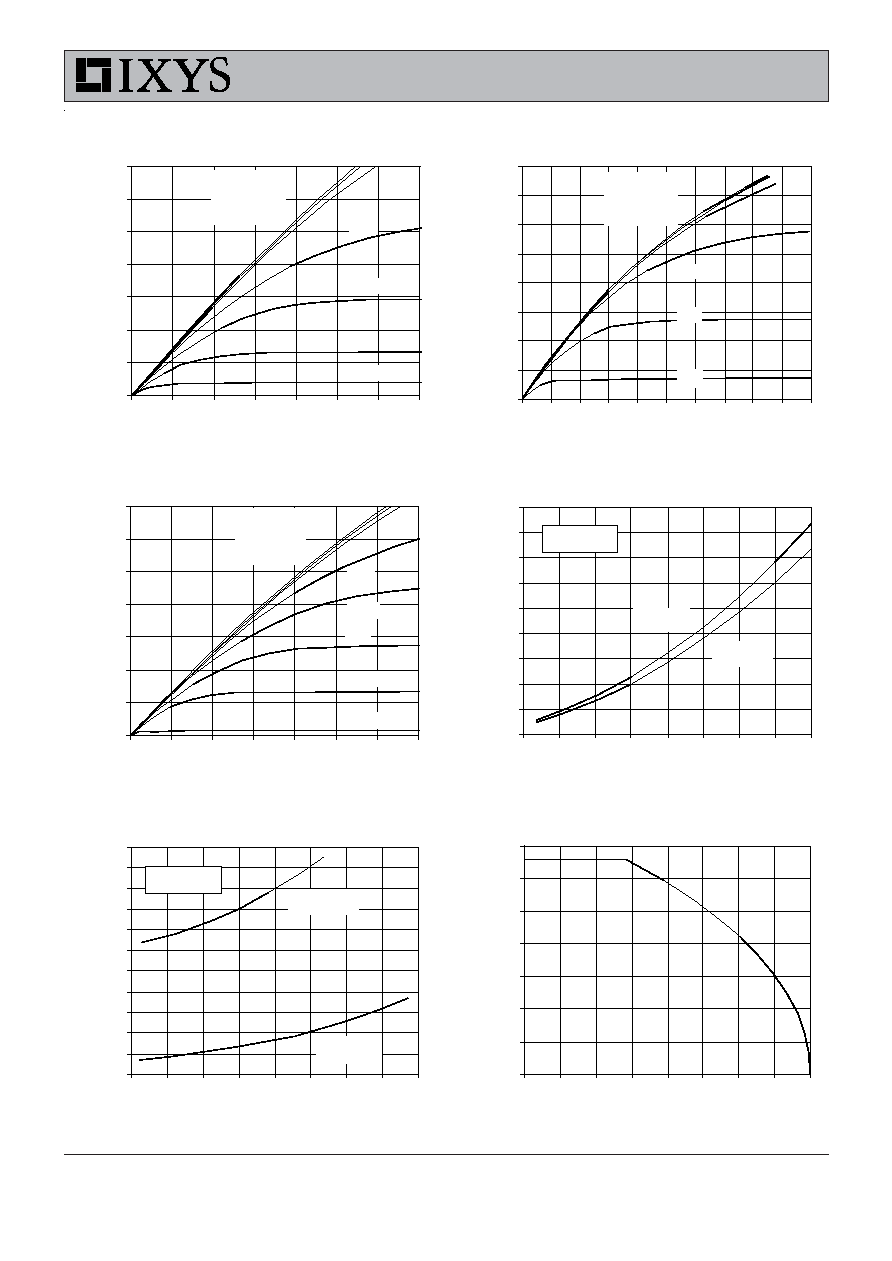
Fig. 2. Extended Output Characteristics
@ 25
ş
C
0
20
40
60
80
100
120
140
160
0
2
4
6
8
10
12
14
16
18
20
V
D S
- Volts
I
D
- A
m
p
e
re
s
V
GS
= 10V
9V
8V
7V
6V
5V
Fig. 3. Output Characteristics
@ 125
ş
C
0
10
20
30
40
50
60
70
0
2
4
6
8
10
12
14
V
D S
- Volts
I
D
- A
m
p
e
r
e
s
V
GS
= 10V
8V
7V
5V
6V
3.5V
4.5V
5.5V
Fig. 1. Output Characteristics
@ 25
ş
C
0
10
20
30
40
50
60
70
0
1
2
3
4
5
6
7
V
D S
- Volts
I
D
- A
m
p
e
re
s
V
GS
= 10V
8V
7V
5V
6V
5.5V
4.5V
Fig. 4. R
DS(on
)
Norm alized to 0.5 I
D25
Value vs. Junction Tem perature
0.4
0.7
1
1.3
1.6
1.9
2.2
2.5
2.8
3.1
-50
-25
0
25
50
75
100
125
150
T
J
- Degrees Centigrade
R
D S
(
o
n
)
-
N
o
r
m
aliz
e
d
I
D
= 66A
I
D
= 33A
V
GS
= 10V
Fig. 6. Drain Current vs. Case
Tem perature
0
10
20
30
40
50
60
70
-50
-25
0
25
50
75
100
125
150
T
C
- Degrees Centigrade
I
D
- A
m
p
e
r
e
s
Fig. 5. R
DS(on)
Norm alized to
0.5 I
D25
Value vs. I
D
0.8
1
1.2
1.4
1.6
1.8
2
2.2
2.4
2.6
2.8
3
0
20
40
60
80
100
120
140
160
I
D
- Amperes
R
D S
(
o
n
)
- N
o
rm
a
l
i
z
e
d
T
J
= 125C
T
J
= 25C
V
GS
= 10V

IXYS reserves the right to change limits, test conditions, and dimensions.
IXFN66N50Q2
Fig. 11. Capacitance
100
1000
10000
0
5
10
15
20
25
30
35
40
V
D S
- Volts
C
a
pa
c
i
t
a
n
c
e -
pi
c
o
F
a
r
a
ds
Ciss
Coss
Crss
f = 1MHz
Fig. 10. Gate Charge
0
1
2
3
4
5
6
7
8
9
10
0
20
40
60
80
100 120 140 160 180 200
Q
G
- nanoCoulombs
V
G S
-
V
o
l
t
s
V
DS
= 250V
I
D
= 33A
I
G
= 10mA
Fig. 7. Input Adm ittance
0
10
20
30
40
50
60
70
80
90
100
3
3.5
4
4.5
5
5.5
6
6.5
7
V
G S
- Volts
I
D
- A
m
p
e
re
s
T
J
= 125C
25C
-40C
Fig. 8. Transconductance
0
10
20
30
40
50
60
70
80
0
20
40
60
80
100
120
I
D
- Amperes
g
f s
-
S
i
e
m
e
n
s
T
J
= -40C
25C
125C
Fig. 9. Source Current vs.
Source-To-Drain Voltage
0
20
40
60
80
100
120
140
160
180
0.4
0.5
0.6
0.7
0.8
0.9
1
1.1
1.2
1.3
V
S D
- Volts
I
S
- A
m
p
e
re
s
T
J
= 125C
T
J
= 25C
Fig. 12. Forw ard-Bias
Safe Operating Area
1
10
100
1000
10
100
1000
V
D S
- Volts
I
D
-
A
m
p
e
re
s
100µs
1ms
DC
T
J
= 150C
T
C
= 25C
R
DS(on)
Limit
10ms
25µs

© 2003 IXYS All rights reserved
IXFN66N50Q2
Fig. 13. Maximum Transient Thermal Resistance
0.00
0.01
0.10
1.00
0.1
1
10
100
1000
10000
Pulse Width - milliseconds
R
( t h ) J
C
-
C /
W