© 2002 IXYS All rights reserved
Symbol
Symbol
Symbol
Symbol
Symbol
Test Conditions
Test Conditions
Test Conditions
Test Conditions
Test Conditions
Maximum Ratings
Maximum Ratings
Maximum Ratings
Maximum Ratings
Maximum Ratings
V
V
V
V
V
DSS
DSS
DSS
DSS
DSS
T
J
= 25
°
C to 150
°
C
1000
V
V
V
V
V
V
DGR
DGR
DGR
DGR
DGR
T
J
= 25
°
C to 150
°
C; R
GS
= 1 M
1000
V
V
V
V
V
V
GS
GS
GS
GS
GS
Continuous
±
20
V
V
V
V
V
V
GSM
GSM
GSM
GSM
GSM
Transient
±
30
V
II
II
I
D25
D25
D25
D25
D25
T
C
= 25
°
C
30
A
II
II
I
DM
DM
DM
DM
DM
T
C
= 25
°
C, Note 1
136
A
II
II
I
AR
AR
AR
AR
AR
T
C
= 25
°
C
34
A
E
E
E
E
E
AR
AR
AR
AR
AR
T
C
= 25
°
C
64
mJ
E
E
E
E
E
AS
AS
AS
AS
AS
T
C
= 25
°
C
4
J
dv/dt
dv/dt
dv/dt
dv/dt
dv/dt
I
S
I
DM
, di/dt
100 A/
µ
s, V
DD
V
DSS
5
V/ns
T
J
150
°
C, R
G
= 2
P
P
P
P
P
D
D
D
D
D
T
C
= 25
°
C
550
W
T
T
T
T
T
J
J
J
J
J
-55 ... +150
°
C
T
T
T
T
T
JM
JM
JM
JM
JM
150
°
C
T
T
T
T
T
stg
stg
stg
stg
stg
-55 ... +150
°
C
T
T
T
T
T
L
L
L
L
L
1.6 mm (0.063 in.) from case for 10 s
300
°
C
V
V
V
V
V
ISOL
ISOL
ISOL
ISOL
ISOL
50/60 Hz, RMS
t = 1 min
2500
V~
I
ISOL
1 mA
t = 1 s
3000
V~
Weight
Weight
Weight
Weight
Weight
5
g
Symbol
Symbol
Symbol
Symbol
Symbol
Test Conditions
Test Conditions
Test Conditions
Test Conditions
Test Conditions
Characteristic Values
Characteristic Values
Characteristic Values
Characteristic Values
Characteristic Values
(T
J
= 25
°
C, unless otherwise specified)
min.
min.
min.
min.
min.
typ.
typ.
typ.
typ.
typ.
max.
max.
max.
max.
max.
V
DSS
V
GS
= 0 V, I
D
= 3mA
1000
V
V
GS(th)
V
DS
= V
GS
, I
D
= 8mA
2.5
5.0 V
II
II
I
GSS
GSS
GSS
GSS
GSS
V
GS
=
±
20 V
DC
, V
DS
= 0
±
100 nA
II
II
I
DSS
DSS
DSS
DSS
DSS
V
DS
= V
DSS
T
J
= 25
°
C
100
µ
A
V
GS
= 0 V
T
J
= 125
°
C
2 mA
R
R
R
R
R
DS(on)
DS(on)
DS(on)
DS(on)
DS(on)
V
GS
= 10 V, I
D
= I
T
0.28
Note 1
98932 (7/02)
ISOPLUS-264
ISOPLUS-264
ISOPLUS-264
ISOPLUS-264
ISOPLUS-264
TM
TM
TM
TM
TM
HiPerFET
HiPerFET
HiPerFET
HiPerFET
HiPerFET
TM
TM
TM
TM
TM
Power MOSFETs
Power MOSFETs
Power MOSFETs
Power MOSFETs
Power MOSFETs
ISOPLUS
ISOPLUS
ISOPLUS
ISOPLUS
ISOPLUS264
264
264
264
264
TM
TM
TM
TM
TM
(Electrically Isolated Backside)
(Electrically Isolated Backside)
(Electrically Isolated Backside)
(Electrically Isolated Backside)
(Electrically Isolated Backside)
Single Die MOSFET
N-Channel Enhancement Mode
Avalanche Rated, High dv/dt, Low t
rr
Features
Features
Features
Features
Features
Silicon chip on Direct-Copper-Bond
substrate
- High power dissipation
- Isolated mounting surface
- 2500V electrical isolation
Low drain to tab capacitance(<30pF)
Low R
DS (on)
HDMOS
TM
process
Rugged polysilicon gate cell structure
Unclamped Inductive Switching (UIS)
rated
Fast intrinsic Rectifier
Applications
Applications
Applications
Applications
Applications
DC-DC converters
Battery chargers
Switched-mode and resonant-mode
power supplies
DC choppers
AC motor control
Advantages
Advantages
Advantages
Advantages
Advantages
Easy assembly
Space savings
High power density
IXFL 34N100
IXFL 34N100
IXFL 34N100
IXFL 34N100
IXFL 34N100 V
V
V
V
V
DSS
DSS
DSS
DSS
DSS
=
==
=
= 1000
1000
1000
1000
1000 V
V
V
V
V
II
II
I
D25
D25
D25
D25
D25
=
==
=
= 30
30
30
30
30 A
A
A
A
A
R
R
R
R
R
DS(on)
DS(on)
DS(on)
DS(on)
DS(on)
=
==
=
= 0.28
0.28
0.28
0.28
0.28
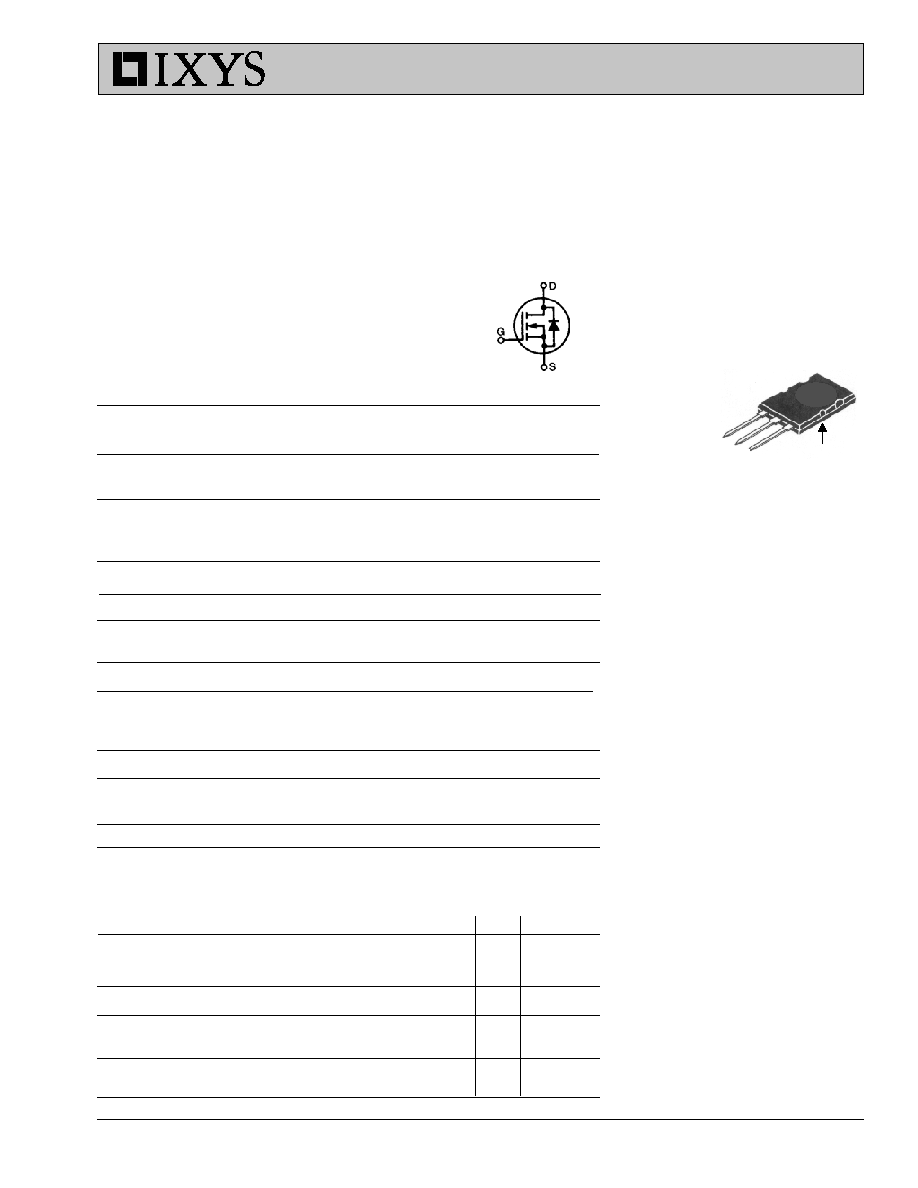
G = Gate
C = Collector
E = Emitter
Tab = Collector
G
C
E
(TAB)
Preliminary Data Sheet
Preliminary Data Sheet
Preliminary Data Sheet
Preliminary Data Sheet
Preliminary Data Sheet
IXYS reserves the right to change limits, test conditions, and dimensions.
IXYS MOSFETs and IGBTs are covered by one or more of the following U.S. patents:
4,835,592
4,881,106
5,017,508
5,049,961
5,187,117
5,486,715
6,306,728B1
4,850,072
4,931,844
5,034,796
5,063,307
5,237,481
5,381,025
Symbol
Symbol
Symbol
Symbol
Symbol
Test Conditions
Test Conditions
Test Conditions
Test Conditions
Test Conditions
Characteristic Values
Characteristic Values
Characteristic Values
Characteristic Values
Characteristic Values
(T
J
= 25
°
C, unless otherwise specified)
min.
min.
min.
min.
min.
typ.
typ.
typ.
typ.
typ.
max.
max.
max.
max.
max.
g
gg
g
g
fs
fs
fs
fs
fs
V
DS
= 15 V; I
D
= I
T
Note 2
18
40
S
C
C
C
C
C
iss
iss
iss
iss
iss
9200
pF
C
C
C
C
C
oss
oss
oss
oss
oss
V
GS
= 0 V, V
DS
= 25 V, f = 1 MHz
1200
pF
C
C
C
C
C
rss
rss
rss
rss
rss
300
pF
tt
tt
t
d(on)
d(on)
d(on)
d(on)
d(on)
41
ns
tt
tt
t
r
r
r
r
r
V
GS
= 10 V, V
DS
= 0.5 · V
DSS
, I
D
= I
T
65
ns
tt
tt
t
d(off)
d(off)
d(off)
d(off)
d(off)
R
G
= 1
(External)
110
ns
tt
tt
t
f
f
f
f
f
30
ns
Q
Q
Q
Q
Q
g(on)
g(on)
g(on)
g(on)
g(on)
380
nC
Q
Q
Q
Q
Q
gs
gs
gs
gs
gs
V
GS
= 10 V, V
DS
= 0.5 · V
DSS
, I
D
= I
T
65
nC
Q
Q
Q
Q
Q
gd
gd
gd
gd
gd
185
nC
R
R
R
R
R
thJC
thJC
thJC
thJC
thJC
0.225 K/W
R
R
R
R
R
thCK
thCK
thCK
thCK
thCK
0.05
K/W
Source-Drain Diode
Source-Drain Diode
Source-Drain Diode
Source-Drain Diode
Source-Drain Diode
Characteristic Values
Characteristic Values
Characteristic Values
Characteristic Values
Characteristic Values
(T
J
= 25
°
C, unless otherwise specified)
Symbol
Symbol
Symbol
Symbol
Symbol
Test Conditions
Test Conditions
Test Conditions
Test Conditions
Test Conditions
min.
min.
min.
min.
min.
typ.
typ.
typ.
typ.
typ.
max.
max.
max.
max.
max.
II
II
I
S
S
S
S
S
V
GS
= 0 V
34
A
II
II
I
SM
SM
SM
SM
SM
Repetitive;
136
A
pulse width limited by T
JM
V
V
V
V
V
SD
SD
SD
SD
SD
I
F
= I
S
, V
GS
= 0 V, Note 1
1.3
V
tt
tt
t
r r
r r
r r
r r
r r
I
F
= I
S
,-di/dt = 100 A/
µ
s, V
R
= 100 V T
J
= 25
°
C
180
ns
Q
Q
Q
Q
Q
RM
RM
RM
RM
RM
T
J
= 125
°
C
330
ns
T
J
= 25
°
C
2
µ
C
II
II
I
RM
RM
RM
RM
RM
8
A
Note: 1. Pulse width limited by T
JM
2. Pulse test, t
300
µ
s, duty cycle d
2 %
3. Test current I
T
= 30A
IXFL 34N100
IXFL 34N100
IXFL 34N100
IXFL 34N100
IXFL 34N100
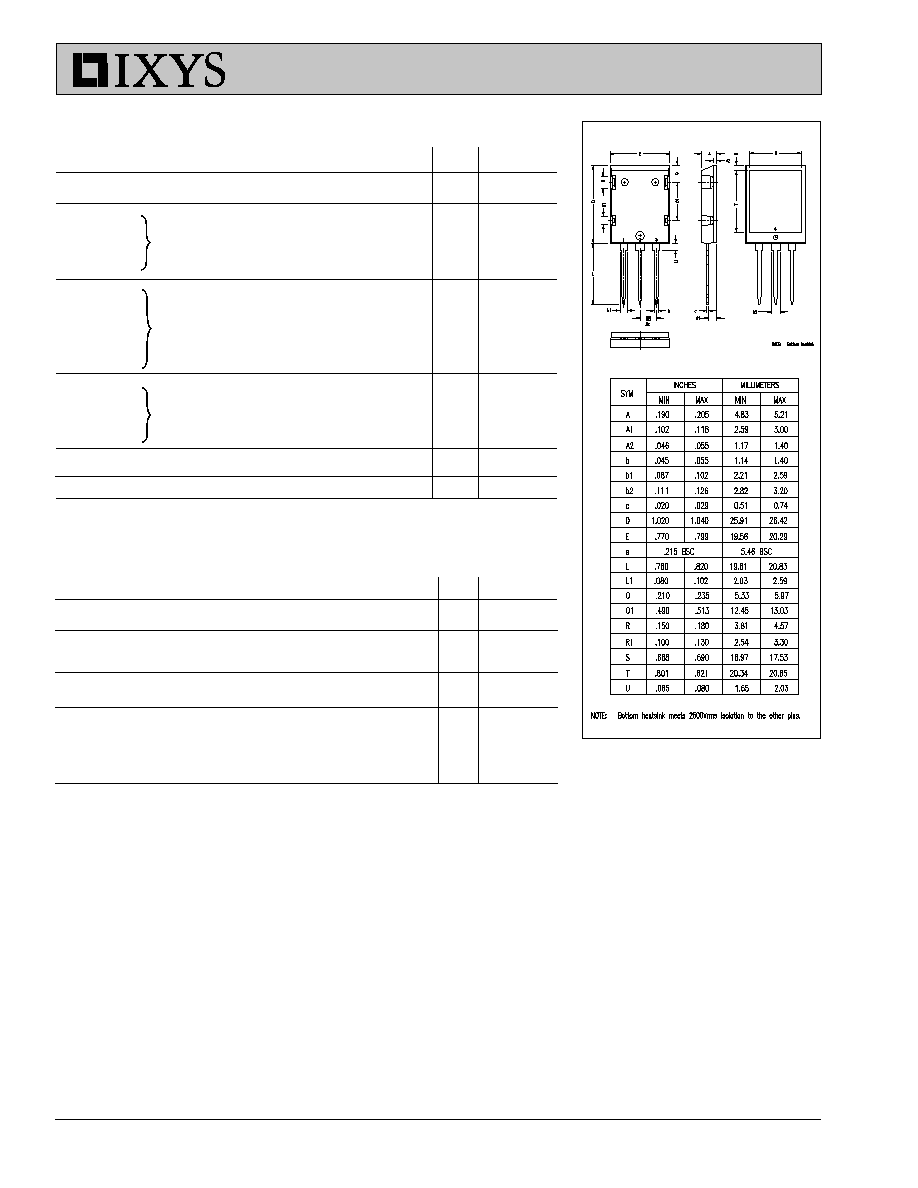
ISOPLUS 264 OUTLINE