© 2004 IXYS All rights reserved
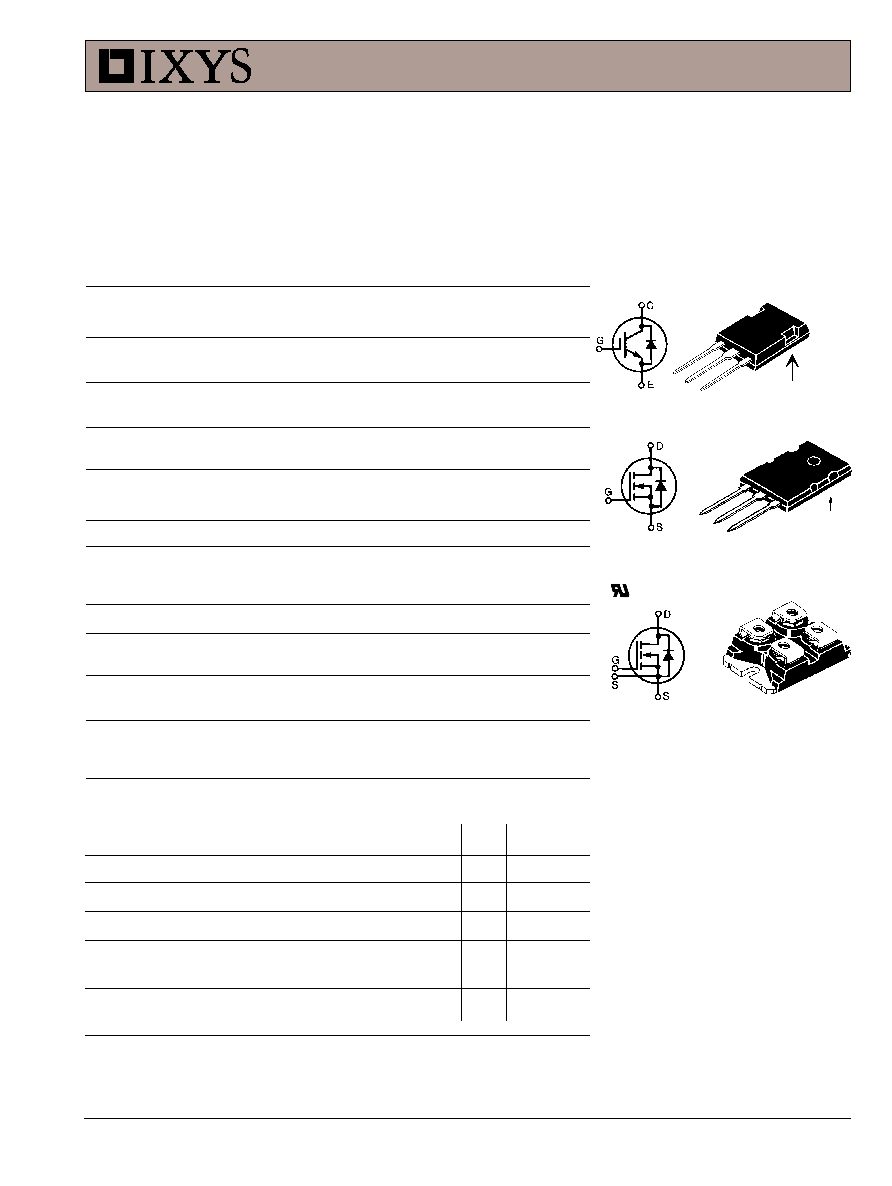
S
G
S
D
miniBLOC, SOT-227 B (IXFN)
E153432
TO-264 AA (IXFK)
Features
·
International standard packages
·
Encapsulating
epoxy
meets
UL
94
V-0, flammability classification
·
miniBLOC
with Aluminium nitride
isolation
·
Low R
DS (on)
HDMOS
TM
process
·
Rugged polysilicon gate cell structure
·
Unclamped Inductive Switching (UIS)
rated
·
Low package inductance
·
Fast intrinsic Rectifier
Advantages
·
PLUS247 package for clip or spring
bar mounting
·
Easy to mount
·
Space savings
·
High power density
G = Gate
D = Drain
S = Source
TAB = Drain
Either Source terminal at miniBLOC can be used
as Main or Kelvin Source
S
G
D
D (TAB)
DS97502G(11/04)
HiPerFET
TM
Power MOSFET
Single Die MOSFET
IXFK 55N50
IXFX 55N50
IXFN 55N50
V
DSS
= 500 V
I
D25
=
55 A
R
DS(on)
= 90m
t
rr
250 ns
PLUS247(IXFX)
G
C
E
(TAB)
Symbol
Test Conditions
Characteristic Values
(T
J
= 25
°C, unless otherwise specified)
Min. Typ.
Max.
V
DSS
V
GS
= 0 V, I
D
= 1 mA
500
V
V
GS(th)
V
DS
= V
GS
, I
D
= 8 mA
2.5
4.5
V
I
GSS
V
GS
=
±20 V
DC
, V
DS
= 0
±200
nA
I
DSS
V
DS
= V
DSS
25
µA
V
GS
= 0 V
T
J
= 125
°C
2
mA
R
DS(on)
V
GS
= 10 V, I
D
= 0.5 I
D25
90
m
Pulse test, t
300 µs, duty cycle d 2 %
Symbol
Test Conditions
Maximum Ratings
V
DSS
T
J
= 25
°C to 150°C
500
V
V
DGR
T
J
= 25
°C to 150°C
500
V
V
GSS
Continuous
±20
V
V
GSM
Transient
±30
V
I
D25
T
C
= 25
°C
55
A
I
DM
T
C
= 25
°C, pulse width limited by T
JM
220
A
I
AR
T
C
= 25
°C
55
A
E
AR
T
C
= 25
°C
60
mJ
dv/dt
I
S
I
DM
, di/dt
100 A/µs, V
DD
V
DSS
10
V/ns
T
J
150°C, R
G
= 4
P
D
T
C
= 25
°C
625
W
T
J
-55 ... +150
°C
T
JM
150
°C
T
stg
-55 ... +150
°C
T
L
1.6 mm (0.062 in.) from case for 10 s (IXFK, IXFX)
300
°C
M
d
Mounting torque
(IXFK, IXFX)
1.13/10 Nm/lb.in.
Terminal leads
(IXFN)
1.13/10 Nm/lb.in.
V
ISOL
50/60 Hz, RMS
(IXFN) t = 1minute
2500
V~
I
ISOL
1 mA
t = 1 s
3000
V~
Weight
PLUS247
5
g
TO-264
10
g
SOT-227B
30
g

Symbol
Test Conditions
Characteristic Values
(T
J
= 25
°C, unless otherwise specified)
Min.
Typ.
Max.
g
fs
V
DS
= 10 V; I
D
= 0.5 · I
D25
Note 1
45
S
C
iss
9400
pF
C
oss
V
GS
= 0 V, V
DS
= 25 V, f = 1 MHz
1280
pF
C
rss
460
pF
t
d(on)
45
ns
t
r
V
GS
= 10 V, V
DS
= 0.5 · V
DSS
, I
D
= 0.5 · I
D25
60
ns
t
d(off)
R
G
= 1
(External),
120
ns
t
f
45
ns
Q
g(on)
330
nC
Q
gs
V
GS
= 10 V, V
DS
= 0.5 · V
DSS
, I
D
= 0.5 · I
D25
55
nC
Q
gd
155
nC
R
thJC
0.20
K/W
R
thCK
IXFK, IXFX
0.15
K/W
R
thCK
0.05
K/W
Source-Drain Diode
(T
J
= 25
°C, unless otherwise specified)
Characteristic Values
Symbol
Test Conditions
Min.
Typ. Max.
I
S
V
GS
= 0
55
A
I
SM
Repetitive;
220
A
pulse width limited by T
JM
V
SD
I
F
= 100 A, V
GS
= 0 V
Note 1
1.5
V
t
rr
250
ns
Q
RM
I
F
= 25 A, -di/dt = 100 A/
µs, V
R
= 100 V
1.0
µC
I
RM
10
A
M4 screws (4x) supplied
Dim.
Millimeter
Inches
Min.
Max.
Min.
Max.
A
31.50
31.88
1.240
1.255
B
7.80
8.20
0.307
0.323
C
4.09
4.29
0.161
0.169
D
4.09
4.29
0.161
0.169
E
4.09
4.29
0.161
0.169
F
14.91
15.11
0.587
0.595
G
30.12
30.30
1.186
1.193
H
38.00
38.23
1.496
1.505
J
11.68
12.22
0.460
0.481
K
8.92
9.60
0.351
0.378
L
0.76
0.84
0.030
0.033
M
12.60
12.85
0.496
0.506
N
25.15
25.42
0.990
1.001
O
1.98
2.13
0.078
0.084
P
4.95
5.97
0.195
0.235
Q
26.54
26.90
1.045
1.059
R
3.94
4.42
0.155
0.174
S
4.72
4.85
0.186
0.191
T
24.59
25.07
0.968
0.987
U
-0.05
0.1
-0.002
0.004
miniBLOC (SOT-227B) Outline
Millimeter
Inches
Min.
Max.
Min.
Max.
A
4.82
5.13
.190
.202
A1
2.54
2.89
.100
.114
A2
2.00
2.10
.079
.083
b
1.12
1.42
.044
.056
b1
2.39
2.69
.094
.106
b2
2.90
3.09
.114
.122
c
0.53
0.83
.021
.033
D
25.91
26.16
1.020
1.030
E
19.81
19.96
.780
.786
e
5.46 BSC
.215 BSC
J
0.00
0.25
.000
.010
K
0.00
0.25
.000
.010
L
20.32
20.83
.800
.820
L1
2.29
2.59
.090
.102
P
3.17
3.66
.125
.144
Q
6.07
6.27
.239
.247
Q1
8.38
8.69
.330
.342
R
3.81
4.32
.150
.170
R1
1.78
2.29
.070
.090
S
6.04
6.30
.238
.248
T
1.57
1.83
.062
.072
Dim.
TO-264 AA Outline
Notes: 1. Pulse test, t
300 µs, duty cycle d 2 %
IXFK55N50
IXFX55N50
IXFN55N50
IXYS reserves the right to change limits, test conditions, and dimensions.
IXYS MOSFETs and IGBTs are covered by
4,835,592
4,931,844
5,049,961
5,237,481
6,162,665
6,404,065 B1
6,683,344
6,727,585
one or moreof the following U.S. patents:
4,850,072
5,017,508
5,063,307
5,381,025
6,259,123 B1
6,534,343
6,710,405B2
6,759,692
4,881,106
5,034,796
5,187,117
5,486,715
6,306,728 B1
6,583,505
6,710,463
Terminals:
1 - Gate
2 - Collector
PLUS247 Outline

© 2004 IXYS All rights reserved
T
C
- Degrees C
-50 -25
0
25
50
75
100 125 150
I
D
- A
m
p
e
re
s
0
10
20
30
40
50
60
T
J
- Degrees C
25
50
75
100
125
150
R
DS
(
O
N
)
- N
o
rm
al
iz
e
d
1.0
1.2
1.4
1.6
1.8
2.0
2.2
V
GS
- Volts
3.0
3.5
4.0
4.5
5.0
5.5
6.0
I
D
- A
m
pe
r
e
s
0
20
40
60
80
100
T
C
- Degrees C
-50 -25
0
25
50
75
100 125 150
I
D
- A
m
p
e
re
s
0
10
20
30
40
50
60
I
D
- Amperes
0
20
40
60
80
100
120
R
DS
(
O
N
)
- N
o
rm
al
iz
e
d
0.8
1.2
1.6
2.0
2.4
2.8
V
DS
- Volts
0
4
8
12
16
20
24
I
D
-
A
m
p
e
re
s
0
20
40
60
80
100
V
DS
- Volts
0
4
8
12
16
20
24
I
D
-
A
m
p
e
re
s
0
20
40
60
80
100
120
140
5V
V
GS
= 10V
V
GS
= 10V
9V
8V
7V
T
J
= 125
O
C
V
GS
= 10V
T
J
= 25
O
C
6V
6V
5V
T
J
= 25
o
C
I
D
= 55A
T
J
= 125
O
C
T
J
= 125
o
C
V
GS
= 10V
9V
8V
7V
I
D
= 27.5A
I
D
- Amperes
0
20
40
60
80
100
120
R
DS
(
O
N
)
- N
o
rm
al
iz
e
d
0.8
1.2
1.6
2.0
2.4
2.8
V
GS
= 10V
V
GS
= 10V
T
J
= 25
O
C
T
J
= 25
o
C
T
J
= 125
O
C
IXF_55N50
IXF_50N50
T
J
= 25
O
C
Figure 1. Output Characteristics at 25
O
C
Figure 2. Output Characteristics at 125
O
C
Figure 3. R
DS(on)
normalized to 0.5
I
D25
value vs. I
D
Figure 4. R
DS(on)
normalized to 0.5
I
D25
value vs. T
J
Figure 5. Drain Current vs. Case Temperature
Figure 6. Admittance Curves
IXFK55N50
IXFX55N50
IXFN55N50
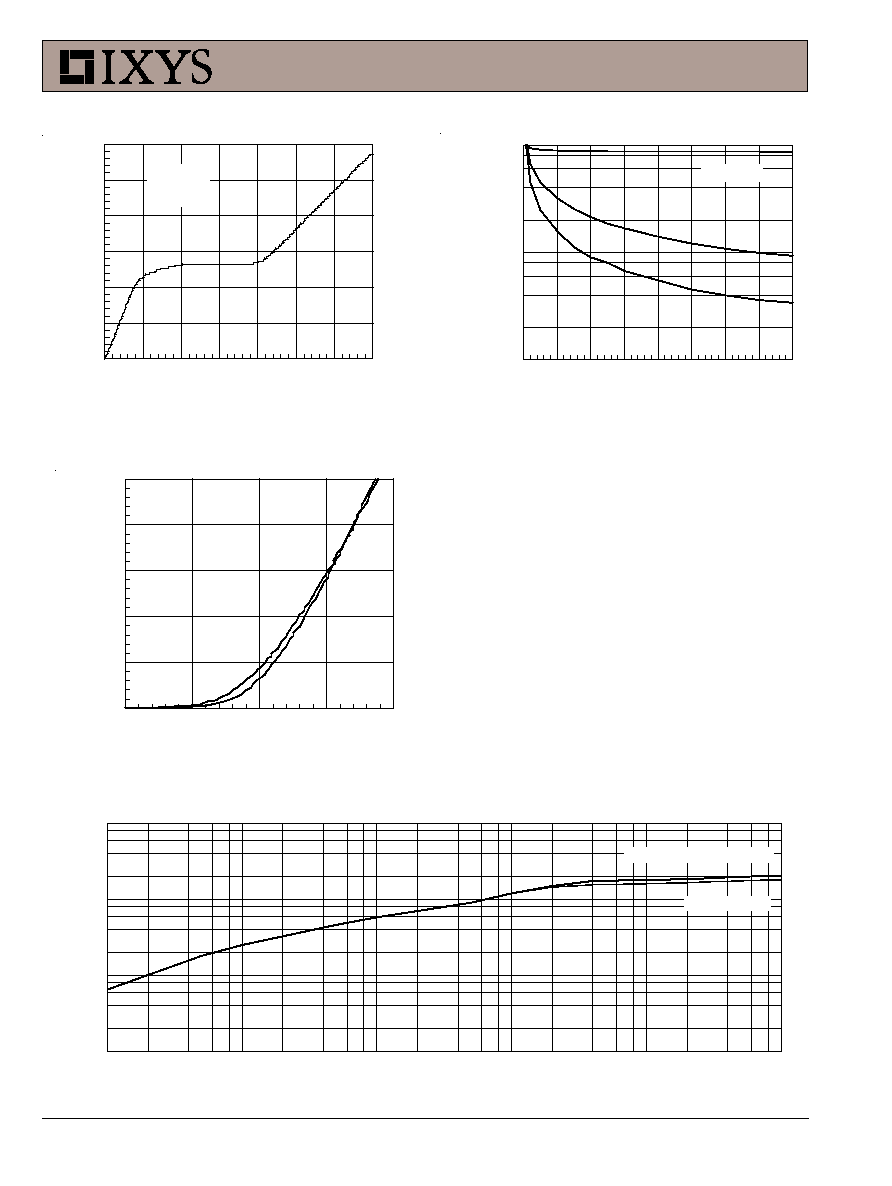
Figure 7. Gate Charge
Figure 8. Capacitance Curves
Figure 9.
Forward Voltage Drop of the
Intrinsic Diode
Figure 10. Transient Thermal Resistance
Gate Charge - nC
0
50
100
150
200
250
300
350
V
GS
- V
o
lts
0
2
4
6
8
10
12
V
DS
= 250V
I
D
= 27.5A
V
DS
- Volts
0
5
10
15
20
25
30
35
40
C
a
pa
cita
nce
- pF
100
1000
10000
Crss
Coss
Ciss
f = 1MHz
V
SD
- Volts
0.2
0.4
0.6
0.8
1.0
I
D
- A
m
pe
r
e
s
0
20
40
60
80
100
T
J
= 125
O
C
T
J
= 25
O
C
IXFK55N50
IXFX55N50
IXFN55N50
Pulse Width - Seconds
10
-4
10
-3
10
-2
10
-1
10
0
10
1
R
(th)
JC
- K
/
W
0.00
0.01
0.10
1.00
IXFK55N50/IXFX55N50
IXFN55N50