1 - 4
© 2000 IXYS All rights reserved
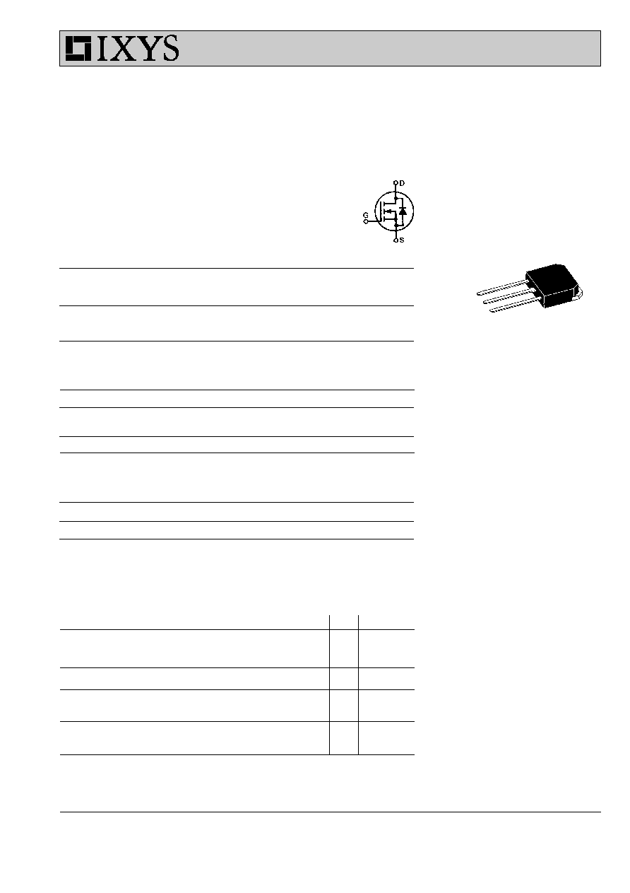
Symbol
Test Conditions
Maximum Ratings
V
DSS
T
J
= 25
°
C to 150
°
C
500
V
V
DGR
T
J
= 25
°
C to 150
°
C; R
GS
= 1 M
W
500
V
V
GS
Continuous
±
20
V
V
GSM
Transient
±
30
V
I
D25
T
C
= 25
°
C
13
A
I
DM
T
C
= 25
°
C, pulse width limited by T
JM
52
A
I
AR
T
C
= 25
°
C
13
A
E
AR
T
C
= 25
°
C
18
mJ
dv/dt
I
S
Ł
I
DM
, di/dt
Ł
100 A/
m
s, V
DD
Ł
V
DSS
,
5
V/ns
T
J
Ł
150
°
C, R
G
= 2
W
P
D
T
C
= 25
°
C
180
W
T
J
-55 ... +150
°
C
T
JM
150
°
C
T
stg
-55 ... +150
°
C
T
L
1.6 mm (0.062 in.) from case for 10 s
300
°
C
Weight
5
g
Symbol
Test Conditions
Characteristic Values
(T
J
= 25
°
C, unless otherwise specified)
min.
typ.
max.
V
DSS
V
GS
= 0 V, I
D
= 250
m
A
500
V
V
GS(th)
V
DS
= V
GS
, I
D
= 2.5 mA
2
4
V
I
GSS
V
GS
=
±
20 V
DC
, V
DS
= 0
±
100
nA
I
DSS
V
DS
= 0.8 · V
DSS
T
J
= 25
°
C
200
m
A
V
GS
= 0 V
T
J
= 125
°
C
1
mA
R
DS(on)
V
GS
= 10 V, I
D
= 0.5 · I
D25
0.4
W
Pulse test, t
Ł
300
m
s, duty cycle d
Ł
2 %
N-Channel Enhancement Mode
High dv/dt, Low t
rr
, HDMOS
TM
Family
G = Gate,
D = Drain,
S = Source,
TAB = Drain
HiPerFET
TM
IXFJ 13N50
V
DSS
= 500 V
Power MOSFETs
I
D (cont)
= 13 A
R
DS(on)
= 0.4
W
t
rr
Ł
250 ns
98578 (2/99)
(TAB)
Features
· Low profile, high power package
· Long creep and strike distances
· Easy up-grade path for TO-220
designs
· Low R
DS (on)
HDMOS
TM
process
· Rugged polysilicon gate cell structure
· Unclamped Inductive Switching (UIS)
rated
· Low package inductance
- easy to drive and to protect
· Fast intrinsic Rectifier
Applications
· DC-DC converters
· Synchronous rectification
· Battery chargers
· Switched-mode and resonant-mode
power supplies
· DC choppers
· AC motor control
· Temperature and lighting controls
· Low voltage relays
Advantages
· High power, low profile package
· Space savings
· High power density
G
D
S
é
IXYS reserves the right to change limits, test conditions, and dimensions.

2 - 4
© 2000 IXYS All rights reserved
Symbol
Test Conditions
Characteristic Values
(T
J
= 25
°
C, unless otherwise specified)
min.
typ.
max.
g
fs
V
DS
= 10 V; I
D
= 0.5 I
D25
, pulse test
7.5
9.0
S
C
iss
2800
pF
C
oss
V
GS
= 0 V, V
DS
= 25 V, f = 1 MHz
300
pF
C
rss
70
pF
t
d(on)
18
30
ns
t
r
V
GS
= 10 V, V
DS
= 0.5 · V
DSS
,
27
40
ns
t
d(off)
I
D
= 0.5 · I
D25
, R
G
= 4.7
W
(External)
76
100
ns
t
f
32
60
ns
Q
g(on)
110
120
nC
Q
gs
V
GS
= 10 V, V
DS
= 0.5 · V
DSS
, I
D
= 0.5 · I
D25
15
25
nC
Q
gd
40
50
nC
R
thJC
0.7
K/W
R
thCK
0.25
K/W
Source-Drain Diode
Characteristic Values
(T
J
= 25
°
C, unless otherwise specified)
Symbol
Test Conditions
min.
typ.
max.
I
S
V
GS
= 0 V
13
A
I
SM
Repetitive; pulse width limited by T
JM
52
A
V
SD
I
F
= I
S
, V
GS
= 0 V,
1.5
V
Pulse test, t
Ł
300
m
s, duty cycle d
Ł
2 %
t
rr
T
J
=
25
°
C
250
ns
T
J
= 125
°
C
350
ns
Q
RM
T
J
=
25
°
C
0.6
m
C
T
J
= 125
°
C
1.25
m
C
I
RM
T
J
=
25
°
C
9
A
T
J
= 125
°
C
15
A
I
F
= I
S
-di/dt = 100 A/
m
s,
V
R
= 100 V
IXFJ 13N50
TO-268 Outline
Dim.
Inches
Millimeters
Min
Max
Min
Max
A
.193
.201
4.90
5.10
A1
.106
.114
2.70
2.90
b
.045
.057
1.15
1.45
b2
.075
.083
1.90
2.10
C
.016
.026
.040
.065
C2
.057
.063
1.45
1.60
D
.543
.551
13.80 14.00
D1
.488
.500
12.40 12.70
E
.624
.632
15.85 16.05
E1
.524
.535
13.30 13.60
e
.215 BSC
5.45 BSC
H
1.365
1.395
34.67 35.43
L
.780
.800
19.81 20.32
L1
.079
.091
2.00
2.30
L2
.039
.045
1.00
1.15
All metal area are
solder plated
1 - gate
2 - drain (collector)
3 - source (emitter)
4 - drain (collector)
IXYS MOSFETS and IGBTs are covered by one or more of the following U.S. patents:
4,835,592
4,881,106
5,017,508
5,049,961
5,187,117
5,486,715
4,850,072
4,931,844
5,034,796
5,063,307
5,237,481
5,381,025

3 - 4
© 2000 IXYS All rights reserved
T
J
- Degrees C
-50
-25
0
25
50
75
100
125
150
BV/
V
G(
t
h
)
- No
rm
a
l
i
z
e
d
0.5
0.6
0.7
0.8
0.9
1.0
1.1
1.2
BV
DSS
T
C
- Degrees C
-50
-25
0
25
50
75
100
125
150
I
D
-
Am
per
es
0.0
2.5
5.0
7.5
10.0
12.5
15.0
T
J
- Degrees C
-50
-25
0
25
50
75
100
125
150
R
DS
(
on)
- N
o
rm
a
l
i
z
e
d
0.50
0.75
1.00
1.25
1.50
1.75
2.00
2.25
2.50
I
D
- Amperes
0
5
10
15
20
25
R
DS
(
on)
- N
o
rm
a
l
i
z
e
d
0.8
0.9
1.0
1.1
1.2
1.3
1.4
V
GS
= 10V
T
J
= 25°C
V
GS
- Volts
0
1
2
3
4
5
6
7
8
9
10
I
D
-
Am
per
es
0
5
10
15
20
25
T
J
= 25°C
V
DS
- Volts
0
5
10
15
20
I
D
-
Am
per
es
0
5
10
15
20
25
6V
5V
7V
8V
V
GS(th)
13N50
I
D
= 6A
V
GS
= 15V
V
GS
=10V
T
J
= 25°C
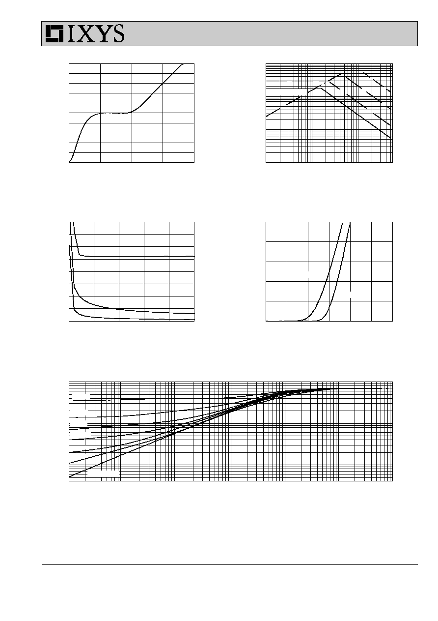
Figure 2. Output Characteristics at
125
O
C
Figure 1. Output Characteristics at 25
O
C
Figure 5. Drain Current vs. Case Temperature
Figure 6. Admittance Curves
Figure 3. R
DS(on)
normalized to 0.5 I
D25
value
Figure 4. R
DS(on)
normalized to 0.5 I
D25
value
IXFJ 13N50
4 - 4
© 2000 IXYS All rights reserved
Figure 8. Capacitance Curves
Figure 7. Gate Charge
Figure 9. Source Current vs. Source
to Drain Voltage
Figure 11. Transient Thermal Resistance
Figure10. Forward Bias Safe Operating
Area
V
SD
- Volt
0.00
0.25
0.50
0.75
1.00
1.25
1.50
I
S
-
Amper
es
0
5
10
15
20
25
Time - Seconds
0.00001
0.0001
0.001
0.01
0.1
1
10
Ther
m
a
l
R
e
sp
onse -
K
/
W
0.01
0.10
1.00
D = 0.2
D=0.02
D = 0.5
D = 0.1
D = 0.05
D=0.01
Single Pulse
V
DS
- Volts
0
5
10
15
20
25
C
apac
i
t
anc
e -
p
F
0
500
1000
1500
2000
2500
3000
3500
4000
C
rss
C
oss
C
iss
Gate Charge - nCoulombs
0
25
50
75
100
V
GS
- V
o
lt
s
0
1
2
3
4
5
6
7
8
9
10
I
D
= 6.5A
V
DS
= 250V
V
DS
- Volts
1
10
100
I
D
-
A
m
per
es
0.1
1
10
100
10µs
100µs
1ms
10ms
100ms
Limited by R
DS(on)
I
G
= 10mA
T
J
= 125°C
T
J
= 25°C
IXFJ 13N50