
1 - 4
© 2000 IXYS All rights reserved
Symbol
Test Conditions
Maximum Ratings
V
DSS
T
J
= 25
°
C to 150
°
C
550
V
V
DGR
T
J
= 25
°
C to 150
°
C; R
GS
= 1 M
W
550
V
V
GS
Continuous
±
20
V
V
GSM
Transient
±
30
V
I
D25
T
C
= 25
°
C
22
A
I
DM
T
C
= 25
°
C, pulse width limited by T
JM
88
A
I
AR
T
C
= 25
°
C
22
A
E
AR
T
C
= 25
°
C
30
mJ
dv/dt
I
S
Ł
I
DM
, di/dt
Ł
100 A/
m
s, V
DD
Ł
V
DSS
,
5
V/ns
T
J
Ł
150
°
C, R
G
= 2
W
P
D
T
C
= 25
°
C
300
W
T
J
-55 ... +150
°
C
T
JM
150
°
C
T
stg
-55 ... +150
°
C
T
L
1.6 mm (0.063 in) from case for 10 s
300
°
C
M
d
Mounting torque
1.13/10
Nm/lb.in.
Weight
6
g
Symbol
Test Conditions
Characteristic Values
(T
J
= 25
°
C, unless otherwise specified)
min.
typ.
max.
V
DSS
V
GS
= 0 V, I
D
= 250
m
A
550
V
V
GS(th)
V
DS
= V
GS
, I
D
= 4 mA
2
4.5
V
I
GSS
V
GS
=
±
20 V
DC
, V
DS
= 0
±
100
nA
I
DSS
V
DS
= 0.8 · V
DSS
T
J
= 25
°
C
250
m
A
V
GS
= 0 V
T
J
= 125
°
C
1
mA
R
DS(on)
V
GS
= 10 V, I
D
= 0.5 · I
D25
0.27
W
Pulse test, t
Ł
300
m
s, duty cycle d
Ł
2 %
TO-247 AD
HiPerFET
TM
IXFH
22
N55
V
DSS
= 550 V
Power MOSFET
I
D (cont)
= 22 A
R
DS(on)
= 0.27
W
t
rr
Ł
250 ns
G = Gate,
D = Drain,
S = Source,
TAB = Drain
N-Channel Enhancement Mode
Avlanche Rated, High dv/dt, Low t
rr
Preliminary data
Features
· International standard packages
JEDEC TO-247 AD
· Low R
DS (on)
HDMOS
TM
process
· Rugged polysilicon gate cell structure
· Unclamped Inductive Switching (UIS)
rated
· Low package inductance (< 5 nH)
- easy to drive and to protect
· Fast intrinsic Rectifier
Applications
· Power Factor Control Circuits
· Uninterruptible Power Supplies (UPS)
· Battery chargers
· Switched-mode and resonant-mode
power supplies
· DC choppers
· Temperature and lighting controls
· Low voltage relays
Advantages
· Easy to mount with 1 screw
(isolated mounting screw hole)
· Space savings
· High power density
D (TAB)
94527A (10/95)
IXYS reserves the right to change limits, test conditions, and dimensions.

2 - 4
© 2000 IXYS All rights reserved
Symbol
Test Conditions
Characteristic Values
(T
J
= 25
°
C, unless otherwise specified)
min.
typ.
max.
g
fs
V
DS
= 10 V; I
D
= 0.5 I
D25
, pulse test
11
18
S
C
iss
4200
pF
C
oss
V
GS
= 0 V, V
DS
= 25 V, f = 1 MHz
450
pF
C
rss
135
pF
t
d(on)
20
40
ns
t
r
V
GS
= 10 V, V
DS
= 0.5 · V
DSS
,
43
60
ns
t
d(off)
I
D
= 0.5 · I
D25
, R
G
= 2
W
(External)
70
90
ns
t
f
40
60
ns
Q
g(on)
150
170
nC
Q
gs
V
GS
= 10 V, V
DS
= 0.5 · V
DSS
, I
D
= 0.5 · I
D25
29
40
nC
Q
gd
60
85
nC
R
thJC
0.42
K/W
R
thCK
0.15
K/W
Source-Drain Diode
Characteristic Values
(T
J
= 25
°
C, unless otherwise specified)
Symbol
Test Conditions
min.
typ.
max.
I
S
V
GS
= 0 V
22
A
I
SM
Repetitive; pulse width limited by T
JM
88
A
V
SD
I
F
= I
S
, V
GS
= 0 V,
1.5
V
Pulse test, t
Ł
300
m
s, duty cycle
d Ł
2 %
t
rr
I
F
= I
S
, -di/dt = 100 A/
m
s, V
R
= 100 V
250
ns
T
J
= 125
°
C
400
ns
TO-247 AD Outline
Dim. Millimeter
Inches
Min.
Max.
Min.
Max.
A
19.81 20.32
0.780 0.800
B
20.80 21.46
0.819 0.845
C
15.75 16.26
0.610 0.640
D
3.55
3.65
0.140 0.144
E
4.32
5.49
0.170 0.216
F
5.4
6.2
0.212 0.244
G
1.65
2.13
0.065 0.084
H
-
4.5
-
0.177
J
1.0
1.4
0.040 0.055
K
10.8
11.0
0.426 0.433
L
4.7
5.3
0.185 0.209
M
0.4
0.8
0.016 0.031
N
1.5
2.49
0.087 0.102
IXFH 22N55
IXYS MOSFETS and IGBTs are covered by one or more of the following U.S. patents:
4,835,592
4,881,106
5,017,508
5,049,961
5,187,117
5,486,715
4,850,072
4,931,844
5,034,796
5,063,307
5,237,481
5,381,025

3 - 4
© 2000 IXYS All rights reserved
IXFH 22N55
Fig. 1 Output Characteristics
Fig. 2 Input Admittance
Fig. 5 Drain Current vs.
Fig. 6 Temperature Dependence of
Case Temperature
Breakdown and Threshold Voltage
Fig. 3 R
DS(on)
vs. Drain Current
Fig. 4 Temperature Dependence
of Drain to Source Resistance
5V
6V
T
J
- Degrees C
-50
-25
0
25
50
75
100
125
150
BV/
V
G(
th
)
- N
o
rm
a
l
ize
d
0.5
0.6
0.7
0.8
0.9
1.0
1.1
1.2
T
C
- Degrees C
0
25
50
75
100
125
150
I
D
- A
m
pe
re
s
0
5
10
15
20
25
T
J
- Degrees C
-50
-25
0
25
50
75
100
125
150
R
DS
(o
n
)
-
N
o
rm
a
l
ize
d
0.50
0.75
1.00
1.25
1.50
1.75
2.00
2.25
2.50
I
D
- Amperes
0
5
10
15
20
25
30
35
40
R
DS
(o
n
)
-
N
o
rm
a
l
ize
d
0.9
1.0
1.1
1.2
1.3
1.4
1.5
V
GS
= 10V
T
J
= 25°C
V
GS
- Volts
0
1
2
3
4
5
6
7
8
9
10
I
D
-
Am
per
e
s
0
10
20
30
40
T
J
= 25°C
V
DS
= 20V
V
DS
- Volts
0
5
10
15
20
I
D
-
Amper
es
0
10
20
30
40
V
GS(th)
V
GS
= 15V
V
GS
= 10V
9V
BV
DSS
V
GS
= 10V
I
D
= 11A
T
J
= 25°C
4 - 4
© 2000 IXYS All rights reserved
IXFH 22N55
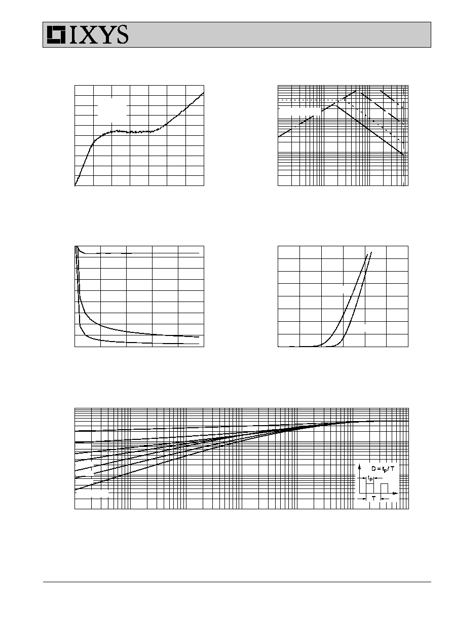
Fig.7 Gate Charge Characteristic Curve
Fig.8 Forward Bias Safe Operating Area
Fig.9 Capacitance Curves
Fig.10 Source Current vs. Source
to Drain Voltage
Fig.11 Transient Thermal Impedance
V
DS
- Volts
1
10
100
I
D
- A
m
p
e
re
s
0.1
1
10
100
Gate Charge - nCoulombs
0
20
40
60
80
100
120
140
V
GE
-
V
o
lts
0
1
2
3
4
5
6
7
8
9
10
V
SD
- Volts
0.00
0.25
0.50
0.75
1.00
1.25
1.50
I
D
-
A
m
p
e
re
s
0
10
20
30
40
50
60
70
80
V
CE
- Volts
0
5
10
15
20
25
Ca
pa
ci
t
a
n
c
e -
pF
0
500
1000
1500
2000
2500
3000
3500
4000
4500
Pulse Width - Seconds
0.00001
0.0001
0.001
0.01
0.1
1
10
T
h
er
m
a
l
Re
sp
on
s
e
-
K
/
W
0.001
0.01
0.1
1
600
D=0.5
C
rss
C
oss
C
iss
V
DS
= 300V
I
D
= 22A
I
G
= 10mA
Limited by R
DS(on)
Single Pulse
T
J
= 125°C
T
J
= 25°C
D=0.2
D=0.01
D=0.02
D=0.05
D=0.1
f = 1 Mhz
V
DS
= 25V
10µs
100µs
1ms
10ms
100ms