© 2002 IXYS All rights reserved
Symbol
Test Conditions
Characteristic Values
(T
J
= 25
°
C, unless otherwise specified)
Min. Typ. Max.
V
DSS
V
GS
= 0 V, I
D
= 3mA
100
V
V
GS(th)
V
DS
= V
GS
, I
D
= 8mA
2
4
V
I
GSS
V
GS
=
±
20V, V
GS
= 0V
±
100
nA
I
DSS
V
DS
= V
DSS
T
J
= 25
°
C
100
µ
A
V
GS
= 0 V
T
J
= 125
°
C
2
mA
R
DS(on)
V
GS
= 10V, I
D
=
I
T
8
m
Note 2
98902 (2/02)
HiPerFET
TM
Power MOSFET
Single Die MOSFET
Symbol Test Conditions
Maximum Ratings
V
DSS
T
J
= 25°C to 150°C
100
V
V
DGR
T
J
= 25°C to 150°C, R
GS
= 1M
100
V
V
GS
Continuous
±
20
V
V
GSM
Transient
±
30
V
I
D25
T
C
= 25
°
C
176
A
I
L(RMS)
Terminal (current limit)
100
A
I
DM
T
C
= 25
°
C; Note 1
720
A
I
AR
T
C
= 25
°
C
180
A
E
AR
T
C
= 25
°
C
60
mJ
E
AS
T
C
= 25
°
C
3
J
dv/dt
I
S
I
DM
, di/dt
100 A/
µ
s, V
DD
V
DSS
5 V/ns
T
J
150
°
C, R
G
= 2
P
D
T
C
= 25
°
C
500
W
T
J
-55 ... +150
°
C
T
JM
150
°
C
T
stg
-55 ... +150
°
C
T
L
1.6 mm (0.063 in) from case for 10 s
300
°
C
V
ISOL
50/60 Hz, RMS
t = 1 min
2500
V~
I
ISOL
1 mA
t = 1 s
3000
V~
M
d
Mounting torque
1.5/13Nm/lb.in.
Terminal connection torque
1.5/13Nm/lb.in.
Weight
19
g
IXFE 180N10
V
DSS
= 100 V
I
D25
= 176 A
R
DS(on)
= 8 m
t
rr
250 ns
Features
·
Conforms to SOT-227B outline
·
Encapsulating
epoxy
meets
UL
94
V-0, flammability classification
·
Low R
DS (on)
HDMOS
TM
process
·
Rugged polysilicon gate cell structure
·
Unclamped Inductive Switching (UIS)
rated
·
Low package inductance
·
Fast intrinsic Rectifier
Applications
·
DC-DC converters
·
Synchronous rectification
·
Battery chargers
·
Switched-mode and resonant-mode
power supplies
·
DC choppers
·
Temperature and lighting controls
·
Low voltage relays
Advantages
·
Easy to mount
·
Space savings
·
High power density
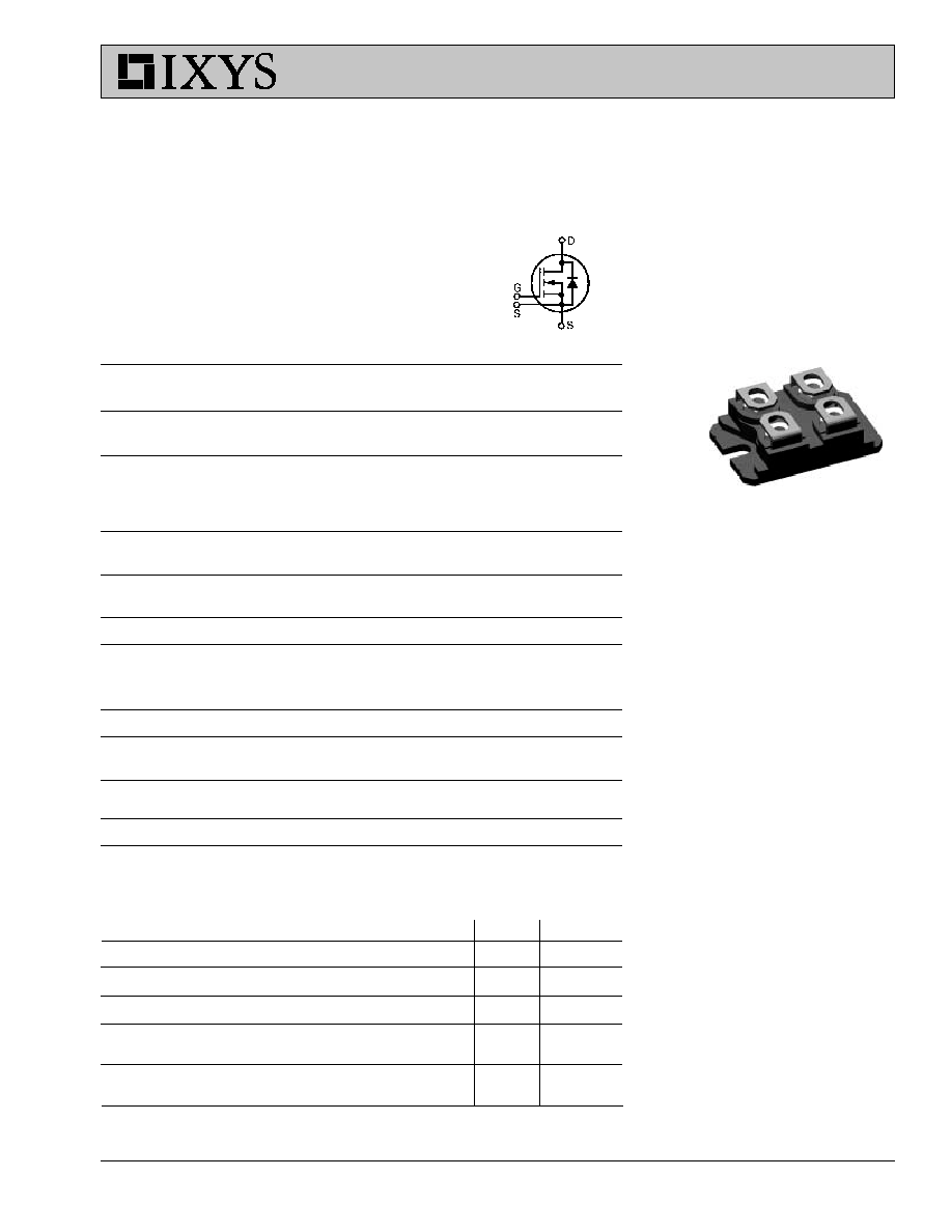
G = Gate
D = Drain
S = Source
Either Source terminal at miniBLOC can be used
as Main or Kelvin Source
Preliminary data sheet
ISOPLUS 227
TM
(IXFE)
S
G
S
D

IXYS reserves the right to change limits, test conditions, and dimensions.
IXYS MOSFETS and IGBTs are covered by one or more of the following U.S. patents:
4,835,592
4,881,106
5,017,508
5,049,961
5,187,117
5,486,715
6,306,728B1
4,850,072
4,931,844
5,034,796
5,063,307
5,237,481
5,381,025
Symbol
Test Conditions
Characteristic Values
(T
J
= 25
°
C, unless otherwise specified)
Min.
Typ.
Max.
g
fs
V
DS
= 10 V; I
D
= 60A, Note 2
60
90
S
C
iss
9100
pF
C
oss
V
GS
= 0 V, V
DS
= 25 V, f = 1 MHz
3200
pF
C
rss
1600
pF
t
d(on)
50
ns
t
r
V
GS
= 10 V, V
DS
= 0.5 · V
DSS
, I
D
=
I
T
90
ns
t
d(off)
R
G
= 1
(External),
140
ns
t
f
65
ns
Q
g(on)
360
nC
Q
gs
V
GS
= 10 V, V
DS
= 0.5 · V
DSS
, I
D
=
I
T
65
nC
Q
gd
190
nC
R
thJC
0.25
K/W
R
thCK
Note:
I
T
= 90 A
0.07
K/W
Source-Drain Diode
(T
J
= 25
°
C, unless otherwise specified)
Characteristic Values
Symbol
Test Conditions
Min.
Typ. Max.
I
S
V
GS
= 0
180
A
I
SM
Repetitive;
720
A
Note1
V
SD
I
F
= 100 A, V
GS
= 0 V,
1.5
V
Note2
t
rr
250
n s
Q
RM
I
F
= 50 A, -di/dt = 100 A/
µ
s, V
R
= 50 V
1.1
µ
C
I
RM
1 3
A
Notes:
1. Pulse width limited by T
JM.
2. Pulse test, t
300 ms, duty cycle d
2 %
3.
I
T
= 90A
IXFE 180N10
ISOPLUS-227 B
Please see IXFN180N10 data
sheet for characteristic curves.