© 2003 IXYS All rights reserved
Symbol
Test Conditions
Maximum Ratings
V
DSS
T
J
= 25
°C to 150°C
800
V
V
DGR
T
J
= 25
°C to 150°C; R
GS
= 1 M
800
V
V
GS
Continuous
±20
V
V
GSM
Transient
±30
V
I
D25
T
C
= 25
°C
13
A
I
DM
T
C
= 25
°C, pulse width limited by T
JM
60
A
I
AR
T
C
= 25
°C
15
A
E
AR
T
C
= 25
°C
30
mJ
E
AS
T
C
= 25
°C
1.0
J
dv/dt
I
S
I
DM
, di/dt
100 A/µs, V
DD
V
DSS
,
10
V/ns
T
J
150°C, R
G
= 2
P
D
T
C
= 25
°C
230
W
T
J
-40 ... +150
° C
T
JM
150
° C
T
stg
-40 ... +150
° C
T
L
1.6 mm (0.062 in.) from case for 10 s
300
° C
Weight
2
g
DS98946B(07/03)
IXFC 15N80Q
V
DSS
= 800 V
I
D25
= 13 A
R
DS(on)
= 0.65
t
rr
250 ns
HiPerFET
TM
ISOPLUS 220
TM
MOSFET
Q-Class
N-Channel Enhancement Mode
Avalanche Rated, High dv/dt, Low Q
g
Features
Silicon chip on Direct-Copper-Bond
substrate
- High power dissipation
- Isolated mounting surface
- 2500V electrical isolation
Low drain to tab capacitance(<35pF)
Low R
DS (on)
Rugged polysilicon gate cell structure
Unclamped Inductive Switching (UIS)
rated
Fast intrinsic Rectifier
Applications
DC-DC converters
Battery chargers
Switched-mode and resonant-mode
power supplies
DC choppers
AC motor control
Advantages
Easy assembly: no screws or isolation
foils required
Space savings
High power density
Electrically Isolated Back Surface
Symbol
Test Conditions
Characteristic Values
(T
J
= 25
°C, unless otherwise specified)
Min. Typ.
Max.
V
DSS
V
GS
= 0 V, I
D
= 3 mA
800
V
V
GS(th)
V
DS
= V
GS
, I
D
= 4 mA
2.0
4.5
V
I
GSS
V
GS
=
±20 V
DC
, V
DS
= 0
±100
nA
I
DSS
V
DS
= V
DSS
T
J
= 25
°C
25
µA
V
GS
= 0 V
T
J
= 125
°C
1
mA
R
DS(on)
V
GS
= 10 V, I
D
= 0.5 I
D25
0.65
Pulse test, t
300 µs, duty cycle d 2 %
V
ISOL
F
C
50/60 Hz, RMS t = 1 min leads to tab 2500 V
mounting force with clip 11...65 / 2.5...15 N/lb
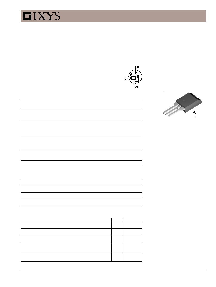
G = Gate
D = Drain
S = Source
G
D
S
ISOPLUS220
TM
Isolated back surface*
See IXFH15N80Q data sheet for
characteristic curves
IXYS reserves the right to change limits, test conditions, and dimensions.
IXFC 15N80Q
IXYS MOSFETs and IGBTs are covered by one or more
of the following U.S. patents:
4,835,592 4,881,106 5,017,508 5,049,961 5,187,117 5,486,715 6,306,728B1 6,259,123B1 6,306,728B1
4,850,072 4,931,844 5,034,796 5,063,307 5,237,481 5,381,025 6,404,065B1 6,162,665 6,534,343
Symbol
Test Conditions
Characteristic Values
(T
J
= 25
°C, unless otherwise specified)
Min.
Typ. Max.
g
fs
V
DS
= 10 V; I
D
= 0.5 I
D25
, pulse test
8
16
S
C
iss
4300
pF
C
oss
V
GS
= 0 V, V
DS
= 25 V, f = 1 MHz
360
pF
C
rss
60
pF
t
d(on)
18
ns
t
r
V
GS
= 10 V, V
DS
= 0.5 V
DSS
, I
D
= 0.5 I
D25
27
ns
t
d(off)
R
G
= 1.5
(External)
53
ns
t
f
16
ns
Q
g(on)
90
nC
Q
gs
V
GS
= 10 V, V
DS
= 0.5 V
DSS
, I
D
= 0.5 I
D25
20
nC
Q
gd
30
nC
R
thJC
0.54
K/W
R
thCK
(TO-247)
0.25
K/W
Source-Drain Diode
Characteristic Values
(T
J
= 25
°C, unless otherwise specified)
Symbol
Test Conditions
min.
typ.
max.
I
S
V
GS
= 0 V
15
A
I
SM
Repetitive;
60
A
V
SD
I
F
= I
S
, V
GS
= 0 V,
1.5
V
Pulse test, t
300 µs, duty cycle d 2 %
t
rr
250
ns
Q
RM
I
F
= I
S
-di/dt = 100 A/
µs, V
R
= 100 V
0.85
µC
I
RM
8
A
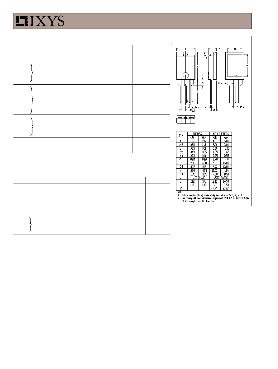
ISOPLUS220 Outline