© 2000 IXYS All rights reserved
1 - 2
HiPerFRED
TM
Epitaxial Diode
with soft recovery
Features
q
International standard package
q
Planar passivated chips
q
Very short recovery time
q
Extremely low switching losses
q
Low I
RM
-values
q
Soft recovery behaviour
q
Epoxy meets UL 94V-0
Applications
q
Antiparallel diode for high frequency
switching devices
q
Antisaturation diode
q
Snubber diode
q
Free wheeling diode in converters
and motor control circuits
q
Rectifiers in switch mode power
supplies (SMPS)
q
Inductive heating
q
Uninterruptible power supplies (UPS)
q
Ultrasonic cleaners and welders
Advantages
q
Avalanche voltage rated for reliable
operation
q
Soft reverse recovery for low
EMI/RFI
q
Low I
RM
reduces:
- Power dissipation within the diode
- Turn-on loss in the commutating
switch
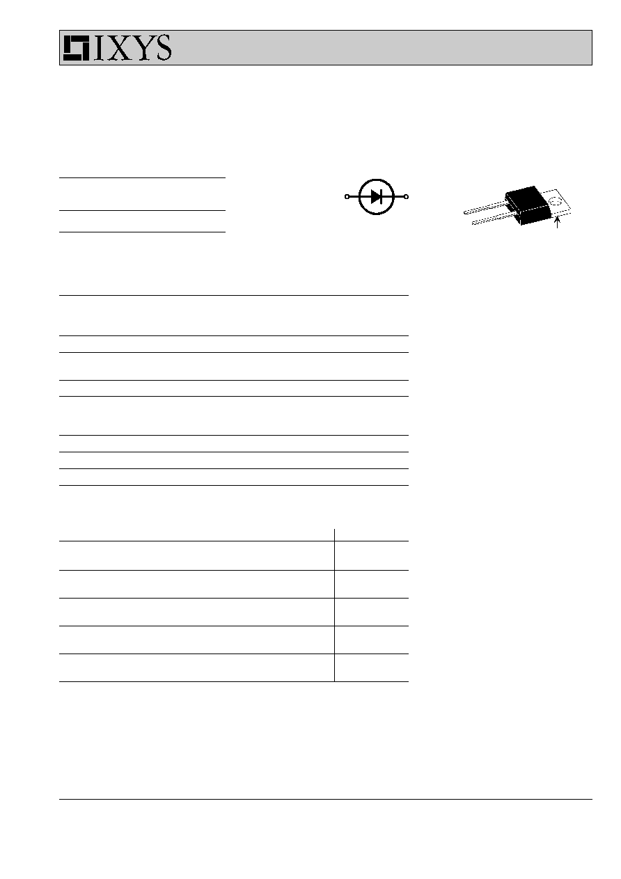
Dimensions see outlines.pdf
C
A
A = Anode, C = Cathode, TAB = Cathode
C
A
TO-220 AC
C (TAB)
Pulse test:
x
Pulse Width = 5 ms, Duty Cycle < 2.0 %
y
Pulse Width = 300
m
s, Duty Cycle < 2.0 %
Data according to IEC 60747 and per diode unless otherwise specified
IXYS reserves the right to change limits, test conditions and dimensions.
DSEP 12-12A
I
FAV
= 15 A
V
RRM
= 1200 V
t
rr
= 40 ns
V
RSM
V
RRM
Type
V
V
1200
1200
DSEP 12-12A
Symbol
Conditions
Maximum Ratings
I
FRMS
35
A
I
FAVM
T
C
= 125°C; rectangular, d = 0.5
15
A
I
FSM
T
VJ
= 45°C; t
p
= 10 ms (50 Hz), sine
90
A
E
AS
T
VJ
= 25°C; non-repetitive
8.7
mJ
I
AS
= 9 A; L = 180 µH
I
AR
V
A
= 1.25·V
R
typ.; f = 10 kHz; repetitive
0.9
A
T
VJ
-55...+175
°C
T
VJM
175
°C
T
stg
-55...+150
°C
P
tot
T
C
= 25°C
95
W
M
d
mounting torque
0.4...0.6
Nm
Weight
typical
2
g
Symbol
Conditions
Characteristic Values
typ.
max.
I
R
x
T
VJ
= 25°C
V
R
= V
RRM
100
m
A
T
VJ
= 150°C V
R
= V
RRM
0.5
mA
V
F
y
I
F
= 15 A;
T
VJ
= 150°C
1.79
V
T
VJ
= 25°C
2.75
V
R
thJC
1.6
K/W
R
thCH
0.5
K/W
t
rr
I
F
= 1 A; -di/dt = 100 A/
m
s;
40
ns
V
R
= 30 V; T
VJ
= 25°C
I
RM
V
R
= 100 V; I
F
= 25 A; -di
F
/dt = 100 A/
m
s
4.5
A
T
VJ
= 100°C
008
© 2000 IXYS All rights reserved
2 - 2
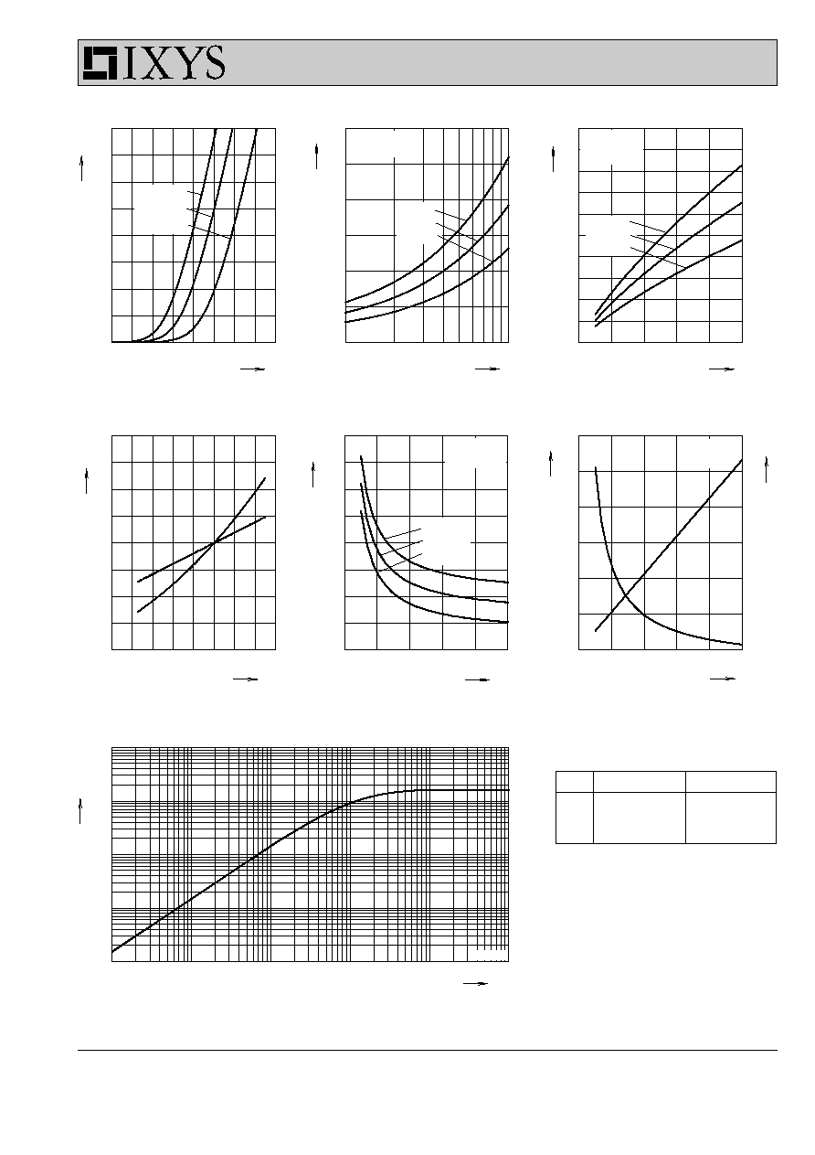
NOTE: Fig. 2 to Fig. 6 shows typical values
DSEP 12-12A
200
600
1000
0
400
800
100
120
140
160
180
0.00001
0.0001
0.001
0.01
0.1
1
0.001
0.01
0.1
1
10
0
40
80
120
160
0.0
0.5
1.0
1.5
2.0
K
f
T
VJ
°C
-di
F
/dt
t
s
K/W
0
200
400
600
800
1000
0
40
80
120
0.0
0.4
0.8
1.2
V
FR
di
F
/dt
V
200
600
1000
0
400
800
0
10
20
30
40
50
100
1000
0.0
0.5
1.0
1.5
2.0
2.5
3.0
0
1
2
3
4
0
5
10
15
20
25
30
35
40
I
RM
Q
r
I
F
A
V
F
-di
F
/dt
-di
F
/dt
A/
m
s
A
V
m
C
A/
m
s
A/
m
s
t
rr
ns
t
fr
Z
thJC
A/
m
s
µ
s
DSEP 12-12A
I
F
= 30A
I
F
= 15A
I
F
= 7.5A
T
VJ
= 100°C
V
R
= 600V
T
VJ
= 100°C
I
F
= 15A
Fig. 3 Peak reverse current I
RM
versus -di
F
/dt
Fig. 2 Reverse recovery charge Q
r
versus -di
F
/dt
Fig. 1 Forward current I
F
versus V
F
T
VJ
= 100°C
V
R
= 600V
T
VJ
= 100°C
V
R
= 600V
I
F
= 30A
I
F
= 15A
I
F
= 7.5A
Q
r
I
RM
Fig. 4 Dynamic parameters Q
r
, I
RM
versus T
VJ
Fig. 5 Recovery time t
rr
versus -di
F
/dt
Fig. 6 Peak forward voltage V
FR
and t
fr
versus di
F
/dt
I
F
= 30A
I
F
= 15A
I
F
= 7.5A
t
fr
V
FR
Fig. 7 Transient thermal resistance junction to case
Constants for Z
thJC
calculation:
i
R
thi
(K/W)
t
i
(s)
1
0.9084
0.0052
2
0.3497
0.0003
3
0.3419
0.0165
T
VJ
=150°C
T
VJ
=100°C
T
VJ
= 25°C
008