
650A
PHASE CONTROL THYRISTORS
Hockey Puk Version
ST300C..C SERIES
1
Bulletin I25157 rev. C 04/00
www.irf.com
Features
Center amplifying gate
Metal case with ceramic insulator
International standard case TO-200AB (E-PUK)
Typical Applications
DC motor controls
Controlled DC power supplies
AC controllers
I
T(AV)
650
A
@ T
hs
55
°C
I
T(RMS)
1290
A
@ T
hs
25
°C
I
TSM
@
50Hz
8000
A
@ 60Hz
8380
A
I
2
t
@
50Hz
320
KA
2
s
@ 60Hz
292
KA
2
s
V
DRM
/V
RRM
400 to 2000
V
t
q
typical
100
µs
T
J
- 40 to 125
°C
Parameters
ST300C..C
Units
Major Ratings and Characteristics
case style TO-200AB (E-PUK)

ST300C..C Series
2
www.irf.com
Bulletin I25157 rev. C 04/00
ST300C..C
50
ELECTRICAL SPECIFICATIONS
Voltage Ratings
Voltage
V
DRM
/V
RRM
, max. repetitive
V
RSM
, maximum non-
I
DRM
/I
RRM
max.
Type number
Code
peak and off-state voltage
repetitive peak voltage
@ T
J
= T
J
max
V
V
mA
04
400
500
08
800
900
12
1200
1300
16
1600
1700
18
1800
1900
20
2000
2100
I
T(AV)
Max. average on-state current
650 (320)
A
180° conduction, half sine wave
@ Heatsink temperature
55 (75)
°C
double side (single side) cooled
I
T(RMS)
Max. RMS on-state current
1290
DC @ 25°C heatsink temperature double side cooled
I
TSM
Max. peak, one-cycle
8000
t = 10ms
No voltage
non-repetitive surge current
8380
A
t = 8.3ms
reapplied
6730
t = 10ms
100% V
RRM
7040
t = 8.3ms
reapplied
Sinusoidal half wave,
I
2
t
Maximum I
2
t for fusing
320
t = 10ms
No voltage
Initial T
J
= T
J
max.
292
t = 8.3ms
reapplied
226
t = 10ms
100% V
RRM
207
t = 8.3ms
reapplied
I
2
t
Maximum I
2
t for fusing
3200
KA
2
s t = 0.1 to 10ms, no voltage reapplied
V
T(TO)1
Low level value of threshold
voltage
V
T(TO)2
High level value of threshold
voltage
r
t1
Low level value of on-state
slope resistance
r
t2
High level value of on-state
slope resistance
V
TM
Max. on-state voltage
2.18
V
I
pk
= 1635A, T
J
= T
J
max, t
p
= 10ms sine pulse
I
H
Maximum holding current
600
I
L
Typical latching current
1000
0.97
(16.7% x
x I
T(AV)
< I <
x I
T(AV)
), T
J
= T
J
max.
0.74
(16.7% x
x I
T(AV)
< I <
x I
T(AV)
), T
J
= T
J
max.
0.73
(I >
x I
T(AV)
),T
J
= T
J
max.
Parameter
ST300C..C
Units Conditions
0.98
(I >
x I
T(AV)
),T
J
= T
J
max.
On-state Conduction
KA
2
s
V
m
mA
T
J
= 25°C, anode supply 12V resistive load
ST300C..C Series
3
www.irf.com
Bulletin I25157 rev. C 04/00
di/dt
Max. non-repetitive rate of rise
Gate drive 20V, 20
, t
r
1µs
of turned-on current
T
J
= T
J
max, anode voltage
80% V
DRM
Gate current 1A, di
g
/dt = 1A/µs
V
d
= 0.67% V
DRM
,
T
J
= 25°C
I
TM
= 300A, T
J
= T
J
max, di/dt
= 40A/µs, V
R
= 50V
dv/dt
= 20V/µs, Gate 0V 100
, t
p
= 500µs
Parameter
ST300C..C
Units Conditions
t
d
Typical delay time
1.0
Switching
t
q
Typical turn-off time
100
µs
1000
A/µs
dv/dt
Maximum critical rate of rise of
off-state voltage
I
RRM
Max. peak reverse and off-state
I
DRM
leakage current
Blocking
500
V/
µs
T
J
= T
J
max, linear to 80% rated V
DRM
Parameter
ST300C..C
Units Conditions
50
mA
T
J
= T
J
max, rated V
DRM
/V
RRM
applied
P
GM
Maximum peak gate power
10.0
T
J
= T
J
max, t
p
5ms
P
G(AV)
Maximum average gate power
2.0
T
J
= T
J
max, f = 50Hz, d% = 50
I
GM
Max. peak positive gate current
3.0
A
T
J
= T
J
max, t
p
5ms
+V
GM
Maximum peak positive
gate voltage
-V
GM
Maximum peak negative
gate voltage
T
J
= - 40°C
mA
T
J
= 25°C
T
J
= 125°C
T
J
= - 40°C
V
T
J
= 25°C
T
J
= 125°C
I
GD
DC gate current not to trigger
10.0
mA
Parameter
ST300C..C
Units Conditions
20
5.0
Triggering
TYP.
MAX.
200
-
100
200
50
-
2.5
-
1.8
3.0
1.1
-
V
GD
DC gate voltage not to trigger
0.25
V
Max. gate current/voltage not to
trigger is the max. value which
will not trigger any unit with rated
V
DRM
anode-to-cathode applied
T
J
= T
J
max
Max. required gate trigger/ cur-
rent/ voltage are the lowest value
which will trigger all units 12V
anode-to-cathode applied
V
GT
DC gate voltage required
to trigger
I
GT
DC gate current required
to trigger
W
V
T
J
= T
J
max, t
p
5ms
ST300C..C Series
4
www.irf.com
Bulletin I25157 rev. C 04/00
T
J
Max. operating temperature range
-40 to 125
T
stg
Max. storage temperature range
-40 to 150
R
thJ-hs
Max. thermal resistance,
0.09
DC operation single side cooled
junction to heatsink
0.04
DC operation double side cooled
R
thC-hs
Max. thermal resistance,
0.02
DC operation single side cooled
case to heatsink
0.01
DC operation double side cooled
F
Mounting force, ± 10%
9800
N
(1000)
(Kg)
wt
Approximate weight
83
g
Parameter
ST300C..C
Units
Conditions
K/W
Thermal and Mechanical Specification
°C
Case style
TO - 200AB (E-PUK)
See Outline Table
K/W
R
thJ-hs
Conduction
(The following table shows the increment of thermal resistence R
thJ-hs
when devices operate at different conduction angles than DC)
Single Side Double Side
Single Side Double Side
180°
0.010
0.011
0.007
0.007
T
J
= T
J
max.
120°
0.012
0.012
0.012
0.013
90°
0.015
0.015
0.016
0.017
K/W
60°
0.022
0.022
0.023
0.023
30°
0.036
0.036
0.036
0.037
Sinusoidal conduction
Rectangular conduction
Conduction angle
Units
Conditions
Ordering Information Table
Device Code
5
1
2
3
4
ST
30
0
C
20
C
1
7
6
8
1
-
Thyristor
2
-
Essential part number
3
-
0 = Converter grade
4
-
C = Ceramic Puk
5
-
Voltage code: Code x 100 = V
RRM
(See Voltage Rating Table)
6
-
C = Puk Case TO-200AB (E-PUK)
7
-
0 = Eyelet terminals (Gate and Auxiliary Cathode Unsoldered Leads)
1 = Fast-on terminals (Gate and Auxiliary Cathode Unsoldered Leads)
2 = Eyelet terminals (Gate and Auxiliary Cathode Soldered Leads)
3 = Fast-on terminals (Gate and Auxiliary Cathode Soldered Leads)
8
-
Critical dv/dt: None = 500V/µsec (Standard value)
L
= 1000V/µsec (Special selection)
ST300C..C Series
5
www.irf.com
Bulletin I25157 rev. C 04/00
Fig. 1 - Current Ratings Characteristics
Fig. 2 - Current Ratings Characteristics
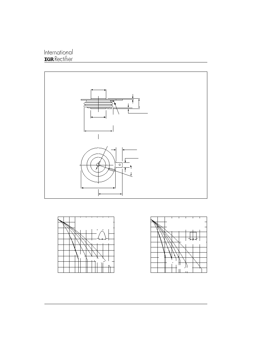
Outline Table
Case Style TO-200AB (E-PUK)
All dimensions in millimeters (inches)
DIA. MAX.
4.75 (0.19)
28 (1.10)
6.5 (0.26)
0.3 (0.01) MIN.
0.3 (0.01) MIN.
ANODE TO GATE
CREEPAGE DISTANCE: 11.18 (0.44) MIN.
STRIKE DISTANCE: 7.62 (0.30) MIN.
25.3 (0.99)
14.1 / 15.1
(0.56 / 0.59)
25°± 5°
GATE TERM. FOR
1.47 (0.06) DIA.
PIN RECEPTACLE
25.3 (0.99)
40.5 (1.59) DIA. MAX.
DIA. MAX.
2 HOLES 3.56 (0.14) x
1.83 (0.07) MIN. DEEP
42 (1.65) MAX.
Quote between upper and lower
pole pieces has to be considered
after application of Mounting Force
(see Thermal and Mechanical
Specification)
Average On-state Current (A)
Maximum Allowable Heatsink Temperature (
°
C)
30
40
50
60
70
80
90
100
110
120
130
0
100
200
300
400
500
30°
60°
90°
120°
180°
Conduction Angle
ST300C..C Series
(Single Side Cooled)
R (DC) = 0.09 K/W
thJ-hs
Average On-state Current (A)
Maximum Allowable Heatsink Temperature (°C)
20
30
40
50
60
70
80
90
100
110
120
130
0
200
400
600
800
DC
30°
60° 90°
120°
180°
Conduction Period
ST300C..C Series
(Single Side Cooled)
R (DC) = 0.09 K/W
thJ-hs

ST300C..C Series
6
www.irf.com
Bulletin I25157 rev. C 04/00
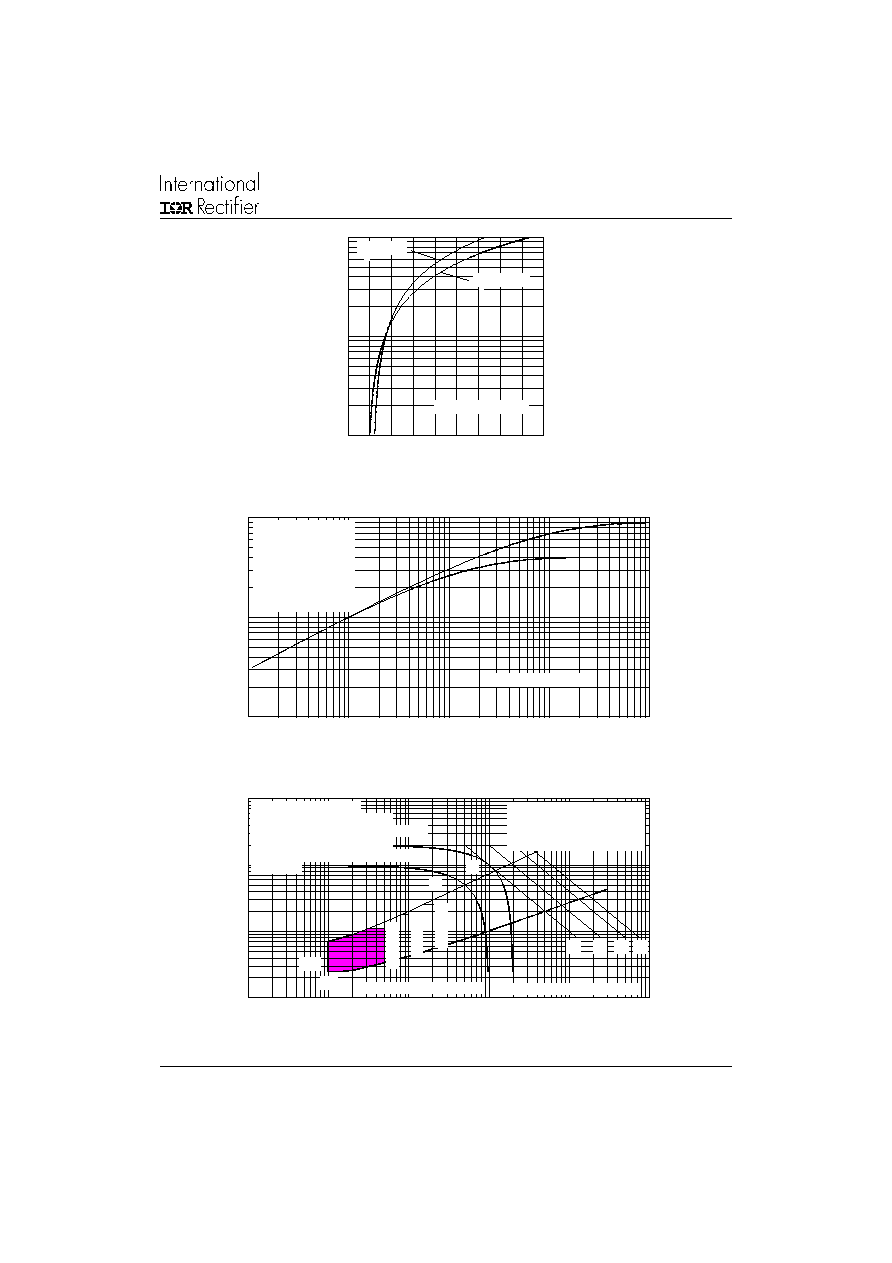
Fig. 3 - Current Ratings Characteristics
Fig. 4 - Current Ratings Characteristics
Fig. 5- On-state Power Loss Characteristics
Fig. 6- On-state Power Loss Characteristics
Fig. 7 - Maximum Non-Repetitive Surge Current
Single and Double Side Cooled
Fig. 8 - Maximum Non-Repetitive Surge Current
Single and Double Side Cooled
Average On-state Current (A)
Maximum Allowable Heatsink Temperature (
°
C)
10
20
30
40
50
60
70
80
90
100
110
120
130
0
200
400
600
800
1000
30°
60°
90°
120°
180°
Conduction Angle
ST300C..C Series
(Double Side Cooled)
R (DC) = 0.04 K/W
thJ-hs
Average On-state Current (A)
Maximum Allowable Heatsink Temperature (
°
C)
20
30
40
50
60
70
80
90
100
110
120
130
0
200 400 600 800 1000 1200 1400
DC
30°
60°
90°
120°
180°
Conduction Period
ST300C..C Series
(Double Side Cooled)
R (DC) = 0.04 K/W
thJ-hs
Average On-state Current (A)
Maximum Average On-state Power Loss (W)
0
200
400
600
800
1000
1200
1400
1600
0
100 200 300 400 500 600 700
180°
120°
90°
60°
30°
RMS Limit
Conduction Angle
ST300C..C Series
T = 125°C
J
Average On-state Current (A)
Maximum Average On-state Power Loss (W)
0
200
400
600
800
1000
1200
1400
1600
1800
0
200
400
600
800 1000 1200
DC
180°
120°
90°
60°
30°
RMS Limit
Conduction Period
ST300C..C Series
T = 125°C
J
Number Of Equal Amplitude Half Cycle Current Pulses (N)
Peak Half Sine Wave On-state Current (A) 3000
3500
4000
4500
5000
5500
6000
6500
7000
7500
1
10
100
Initial T = 125°C
@ 60 Hz 0.0083 s
@ 50 Hz 0.0100 s
J
ST300C..C Series
At Any Rated Load Condition And With
Rated V Applied Following Surge.
RRM
Peak Half Sine Wave On-state Current (A)
Pulse Train Duration (s)
3000
3500
4000
4500
5000
5500
6000
6500
7000
7500
8000
0.01
0.1
1
Versus Pulse Train Duration. Control
Initial T = 125°C
No Voltage Reapplied
Rated V Reapplied
RRM
J
ST300C..C Series
Maximum Non Repetitive Surge Current
Of Conduction May Not Be Maintained.
ST300C..C Series
7
www.irf.com
Bulletin I25157 rev. C 04/00
Fig. 9 - On-state Voltage Drop Characteristics
Fig. 10 - Thermal Impedance Z
thJ-hs
Characteristics
Fig. 11 - Gate Characteristics
Instantaneous On-state Voltage (V)
Instantaneous On-state Current (A)
Square Wave Pulse Duration (s)
Transient Thermal Impedance Z
thJ-hs
(K/W)
Instantaneous Gate Current (A)
Instantaneous Gate Voltage (V)
100
1000
10000
0
1
2
3
4
5
6
7
8
9
T = 25°C
J
T = 125°C
J
ST300C..C Series
0.001
0.01
0.1
0.001
0.01
0.1
1
10
Steady State Value
R = 0.09 K/W
(Single Side Cooled)
R = 0.04 K/W
(Double Side Cooled)
(DC Operation)
ST300C..C Series
thJ-hs
thJ-hs
0.1
1
10
100
0.001
0.01
0.1
1
10
100
VGD
IGD
(b)
(a)
Tj
=25
°
C
Tj
=125
°
C
Tj
=-
40
°
C
(2) (3)
a) Recommended load line for
b) Recommended load line for
<=30% rated di/dt : 10V, 10ohms
Frequency Limited by PG(AV)
rated di/dt : 20V, 10ohms; tr<=1 µs
tr<=1 µs
(1)
(1) PGM = 10W, tp = 4ms
(2) PGM = 20W, tp = 2ms
(3) PGM = 40W, tp = 1ms
(4) PGM = 60W, tp = 0.66ms
Device: ST300C..C Series
Rectangular gate pulse
(4)