
390A
INVERTER GRADE THYRISTORS
Hockey Puk Version
ST223C..C SERIES
1
Bulletin I25174 rev. B 04/00
www.irf.com
Typical Applications
Inverters
Choppers
Induction heating
All types of force-commutated converters
Features
Metal case with ceramic insulator
International standard case TO-200AB (A-PUK)
All diffused design
Center amplifying gate
Guaranteed high dV/dt
Guaranteed high dI/dt
High surge current capability
Low thermal impedance
High speed performance
case style TO-200AB (A-PUK)
I
T(AV)
390
A
@ T
hs
55
°C
I
T(RMS)
745
A
@ T
hs
25
°C
I
TSM
@
50Hz
5850
A
@ 60Hz
6130
A
I
2
t
@
50Hz
171
KA
2
s
@ 60Hz
156
KA
2
s
V
DRM
/V
RRM
400 to 800
V
t
q
range
10 to 30
µs
T
J
- 40 to 125
°
C
Parameters
ST223C..C
Units
Major Ratings and Characteristics
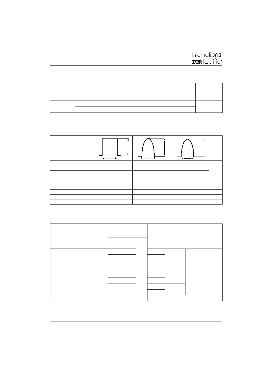
ST223C..C Series
2
www.irf.com
Bulletin I25174 rev. B 04/00
Voltage
V
DRM
/V
RRM
, maximum
V
RSM
, maximum
I
DRM
/I
RRM
max.
Type number
Code
repetitive peak voltage
non-repetitive peak voltage
@ T
J
= T
J
max.
V
V
mA
04
400
500
08
800
900
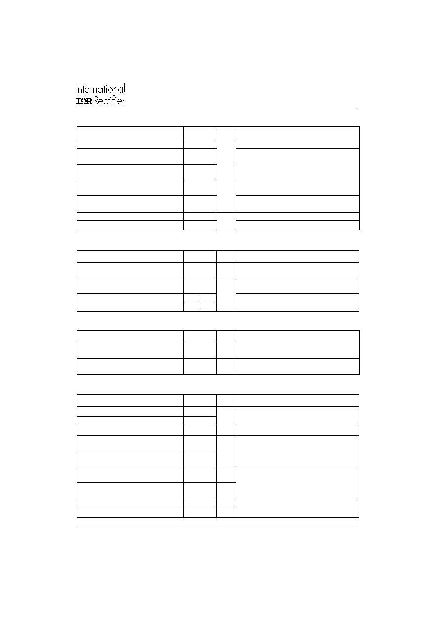
ELECTRICAL SPECIFICATIONS
Voltage Ratings
ST223C..C
40
Frequency
Units
50Hz
930
800
1430
1220
5870
5240
400Hz
910
770
1490
1300
3120
2740
1000Hz
780
650
1430
1260
1880
1640
A
2500Hz
490
400
1070
920
1000
860
Recovery voltage Vr
50
50
50
50
50
50
Voltage before turn-on Vd
V
DRM
V
DRM
V
DRM
Rise of on-state current di/dt
50
50
-
-
-
-
A/
µs
Heatsink temperature
40
55
40
55
40
55
°C
Equivalent values for RC circuit
47
/ 0.22µF
47
/ 0.22µF
47
/ 0.22µF
I
TM
180
o
el
180
o
el
100
µs
I
TM
I
TM
Current Carrying Capability
V
I
T(AV)
Max. average on-state current
390 (150)
A
180° conduction, half sine wave
@ Heatsink temperature
55 (85)
°C
double side (single side) cooled
I
T(RMS)
Max. RMS on-state current
745
DC @ 25°C heatsink temperature double side cooled
I
TSM
Max. peak, one half cycle,
5850
t = 10ms
No voltage
non-repetitive surge current
6130
A
t = 8.3ms
reapplied
4920
t = 10ms
100% V
RRM
5150
t = 8.3ms
reapplied
Sinusoidal half wave,
I
2
t
Maximum I
2
t for fusing
171
t = 10ms
No voltage
Initial T
J
= T
J
max
156
t = 8.3ms
reapplied
121
t = 10ms
100% V
RRM
110
t = 8.3ms
reapplied
I
2
t
Maximum I
2
t for fusing
1710
KA
2
s
t = 0.1 to 10ms, no voltage reapplied
Parameter
ST223C..C
Units
Conditions
On-state Conduction
KA
2
s
ST223C..C Series
3
www.irf.com
Bulletin I25174 rev. B 04/00
V
TM
Max. peak on-state voltage
1.58
I
TM
= 600A, T
J
= T
J
max, t
p
= 10ms sine wave pulse
V
T(TO)1
Low level value of threshold
voltage
V
T(TO)2
High level value of threshold
voltage
r
t
1
Low level value of forward
slope resistance
r
t
2
High level value of forward
slope resistance
I
H
Maximum holding current
600
T
J
= 25°C, I
T
> 30A
I
L
Typical latching current
1000
T
J
= 25°C, V
A
= 12V, Ra = 6
, I
G
= 1A
Parameter
ST223C..C
Units
Conditions
On-state Conduction
1.05
(16.7% x
x I
T(AV)
< I <
x I
T(AV)
), T
J
= T
J
max.
1.09
(I >
x I
T(AV)
), T
J
= T
J
max.
V
0.88
(16.7% x
x I
T(AV)
< I <
x I
T(AV)
), T
J
= T
J
max.
0.82
(I >
x I
T(AV)
), T
J
= T
J
max.
m
mA
di/dt
Max. non-repetitive rate of rise
T
J
= T
J
max, V
DRM
= rated V
DRM
of turned-on current
I
TM
= 2 x di/dt
T
J
= 25°C, V
DM
= rated V
DRM
,
I
TM
= 50A DC, t
p
= 1µs
Resistive load, Gate pulse: 10V, 5
source
T
J
= T
J
max,
I
TM
= 300A, commutating di/dt
= 20A/µs
V
R
= 50V, t
p
= 500µs, dv/dt: see table in device code
Switching
Parameter
ST223C..C
Units
Conditions
1000
A/µs
t
d
Typical delay time
0.78
dv/dt
Maximum critical rate of rise of
T
J
= T
J
max. linear to 80% V
DRM
, higher value
off-state voltage
available on request
I
RRM
Max. peak reverse and off-state
I
DRM
leakage current
Parameter
ST223C..C
Units
Conditions
Blocking
500
V/
µs
40
mA
T
J
= T
J
max, rated V
DRM
/V
RRM
applied
P
GM
Maximum peak gate power
60
P
G(AV)
Maximum average gate power
10
I
GM
Max. peak positive gate current
10
A
T
J
= T
J
max, t
p
5ms
+V
GM
Maximum peak positive
gate voltage
-V
GM
Maximum peak negative
gate voltage
I
GT
Max. DC gate current required
to trigger
V
GT
Max. DC gate voltage required
to trigger
I
GD
Max. DC gate current not to trigger
20
mA
V
GD
Max. DC gate voltage not to trigger
0.25
V
Triggering
Parameter
ST223C..C
Units
Conditions
20
5
V
T
J
= T
J
max, t
p
5ms
200
mA
3
V
T
J
= 25°C, V
A
= 12V, Ra = 6
T
J
= T
J
max, rated V
DRM
applied
10
30
µs
W
T
J
= T
J
max, f = 50Hz, d% = 50
t
q
Max. turn-off time
Min
Max

ST223C..C Series
4
www.irf.com
Bulletin I25174 rev. B 04/00
T
J
Max. operating temperature range
-40 to 125
T
stg
Max. storage temperature range
-40 to 150
R
thJ-hs
Max. thermal resistance,
0.17
DC operation single side cooled
junction to heatsink
0.08
DC operation double side cooled
R
thC-hs
Max. thermal resistance,
0.033
DC operation single side cooled
case to heatsink
0.017
DC operation double side cooled
F
Mounting force, ± 10%
4900
N
(500)
(Kg)
wt
Approximate weight
50
g
Parameter
ST223C..C
Units
Conditions
K/W
Thermal and Mechanical Specification
°C
Case style
TO - 200AB (A-PUK)
See Outline Table
K/W
Single Side Double Side
Single Side Double Side
180°
0.015
0.017
0.011
0.011
120°
0.019
0.019
0.019
0.019
90°
0.024
0.024
0.026
0.026
K/W
T
J
= T
J
max.
60°
0.035
0.035
0.036
0.037
30°
0.060
0.060
0.060
0.061
Sinusoidal conduction
Rectangular conduction
Conduction angle
Units
Conditions
R
thJ-hs
Conduction
(The following table shows the increment of thermal resistence R
thJ-hs
when devices operate at different conduction angles than DC)
Ordering Information Table
ST
22
3
C
08
C
H
K
1
Device Code
5
6
8
9
3
4
10
7
1
2
1
- Thyristor
2
- Essential part number
3
- 3 = Fast turn off
4
- C = Ceramic Puk
5
- Voltage code: Code x 100 = V
RRM
(See Voltage Rating Table)
6
- C = Puk Case TO-200AB (A-PUK)
7
- Reapplied dv/dt code (for t
q
test condition)
8
- t
q
code
9
- 0 = Eyelet term. (Gate and Aux. Cathode Unsoldered Leads)
1 = Fast-on term. (Gate and Aux. Cathode Unsoldered Leads)
2 = Eyelet term. (Gate and Aux. Cathode Soldered Leads)
3 = Fast-on term. (Gate and Aux. Cathode Soldered Leads)
- Critical dv/dt:
None = 500V/µsec (Standard value)
L
= 1000V/µsec (Special selection)
dv/dt - t
q
combinations available
dv/dt (V/µs)
20
50
100
200
400
10
CN
DN
EN
FN *
--
12
CM
DM
EM
FM
--
15
CL
DL
EL
FL *
HL
18
CP
DP
EP
FP
HP
20
CK
DK
EK
FK
HK
25
--
--
--
--
HJ
30
--
--
--
--
HH
t
q
(µs)
*
Standard part number.
All other types available only on request.
10
ST223C..C Series
5
www.irf.com
Bulletin I25174 rev. B 04/00
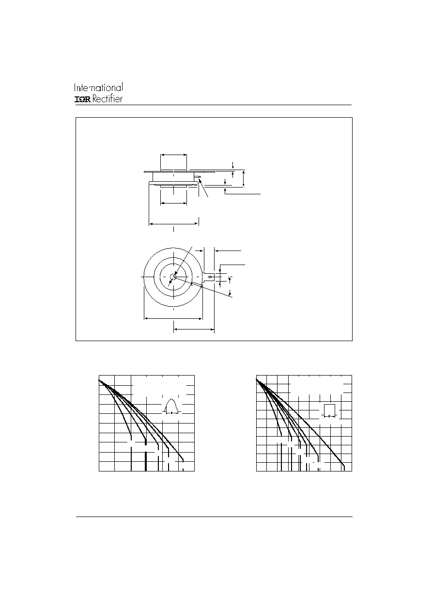
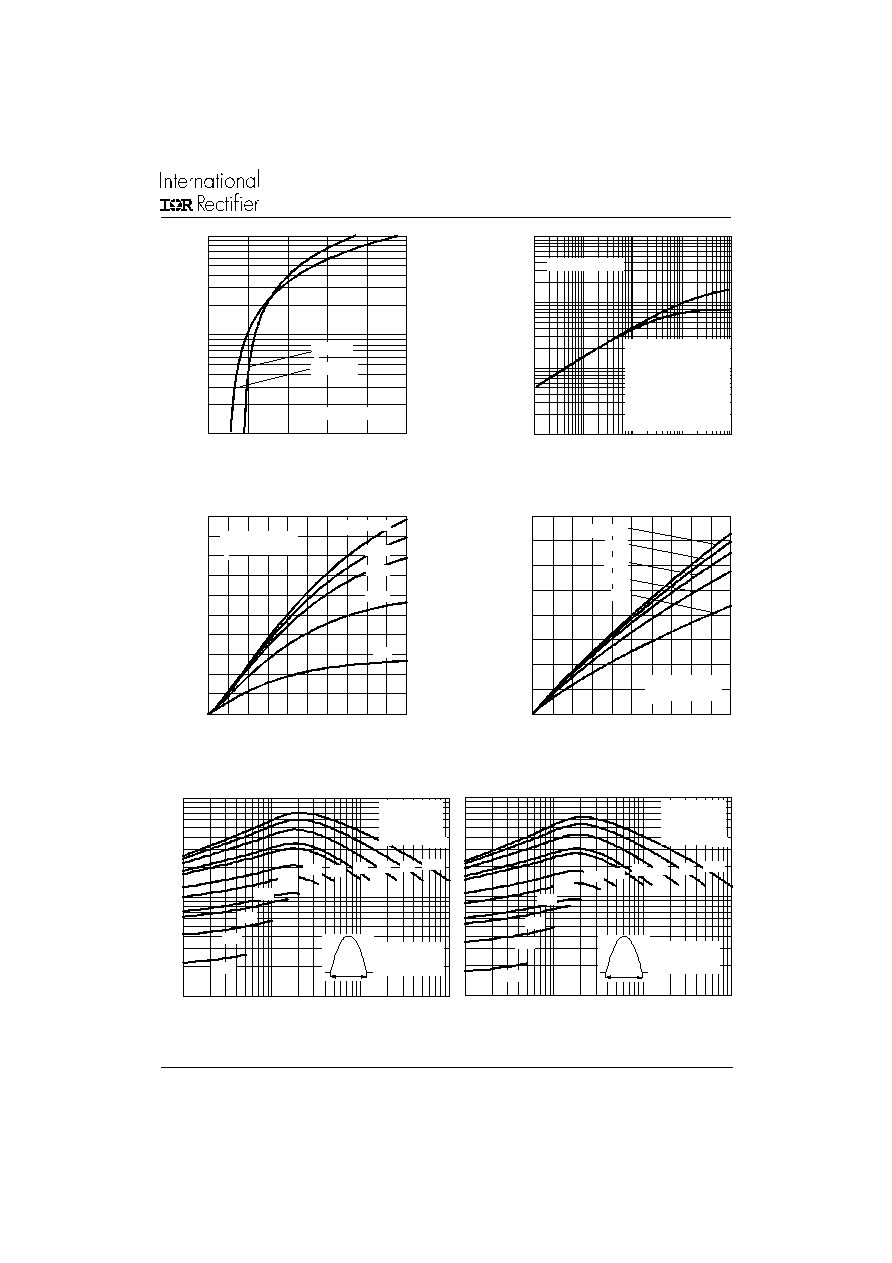
Fig. 1 - Current Ratings Characteristics
Fig. 2 - Current Ratings Characteristics
2 0
3 0
4 0
5 0
6 0
7 0
8 0
9 0
1 0 0
1 1 0
1 2 0
1 3 0
0
5 0 1 0 0 1 5 0 2 0 0 2 5 0 3 0 0 3 5 0 4 0 0 4 5 0
D C
3 0 °
6 0 °
9 0 °
1 2 0 °
1 8 0 °
A v e ra g e O n -s ta t e C u rre n t ( A )
C o nd u ctio n Pe rio d
M
a
x
i
m
u
m
A
l
l
o
w
a
bl
e
He
at
s
i
n
k
T
e
m
p
e
r
at
u
r
e
(
°
C
)
ST 2 2 3 C ..C S e rie s
( Sin g le S id e C o o le d )
R ( D C ) = 0 .1 7 K / W
t hJ- hs
3 0
4 0
5 0
6 0
7 0
8 0
9 0
1 0 0
1 1 0
1 2 0
1 3 0
0
5 0
1 0 0
1 5 0
2 0 0
2 5 0
3 0 0
3 0 °
6 0 °
9 0 °
1 2 0 °
1 8 0 °
A v e ra g e O n -st a t e C u rre n t ( A )
C o nd uc tio n A ng le
M
a
x
i
m
u
m
A
l
l
o
w
a
b
l
e
H
e
a
t
s
i
n
k
T
e
m
p
er
a
t
u
r
e (
°
C)
ST 2 2 3 C ..C S e rie s
( Sin g le S id e C o o le d )
R ( D C ) = 0 .1 7 K / W
thJ - hs
Outline Table
Case Style TO-200AB (A-PUK)
All dimensions in millimeters (inches)
DIA. MAX.
4.75 (0.19)
28 (1.10)
6.5 (0.26)
19 (0.75)
0.3 (0.01) MIN.
0.3 (0.01) MIN.
13.7 / 14.4
(0.54 / 0.57)
25°± 5°
GATE TERM. FOR
1.47 (0.06) DIA.
PIN RECEPTACLE
ANODE TO GATE
CREEPAGE DISTANCE: 7.62 (0.30) MIN.
STRIKE DISTANCE: 7.12 (0.28) MIN.
19 (0.75)
DIA. MAX.
38 (1.50) DIA MAX.
2 HOLES 3.56 (0.14) x
1.83 (0.07) MIN. DEEP
42 (1.65) MAX.
Quote between upper and lower
pole pieces has to be considered
after application of Mounting Force
(see Thermal and Mechanical
Specification)
ST223C..C Series
6
www.irf.com
Bulletin I25174 rev. B 04/00
Fig. 3 - Current Ratings Characteristics
Fig. 4 - Current Ratings Characteristics
Fig. 5 - On-state Power Loss Characteristics
Fig. 6 - On-state Power Loss Characteristics
Fig. 7 - Maximum Non-repetitive Surge Current
Single and Double Side Cooled
Fig. 8 - Maximum Non-repetitive Surge Current
Single and Double Side Cooled
2 0
3 0
4 0
5 0
6 0
7 0
8 0
9 0
1 0 0
1 1 0
1 2 0
1 3 0
0
1 0 0 2 0 0 3 0 0 4 0 0 5 0 0 6 0 0 7 0 0 8 0 0
D C
3 0 °
6 0 °
9 0 °
1 2 0 °
1 8 0 °
A v e ra g e O n -st a te C u rre n t ( A )
C o nd u ction Pe rio d
M
a
x
i
m
u
m
A
l
l
o
w
a
b
l
e H
e
a
t
s
i
n
k
T
e
m
p
er
a
t
u
r
e
(
°
C)
ST 2 2 3 C ..C S e rie s
( D o ub le Sid e C o o le d )
R ( D C ) = 0 .0 8 K/ W
thJ - hs
2 0
3 0
4 0
5 0
6 0
7 0
8 0
9 0
1 0 0
1 1 0
1 2 0
1 3 0
0
1 0 0
2 0 0
3 0 0
4 0 0
5 0 0
3 0 °
6 0 °
9 0 °
1 2 0 °
1 8 0 °
A v e ra g e O n -st a t e C u rre n t ( A )
C o nd uc tion An gle
M
a
x
i
m
u
m
A
l
l
o
w
a
bl
e
He
at
s
i
n
k
T
e
m
p
e
r
at
u
r
e
(
°
C)
S T 2 2 3 C ..C S e rie s
( D o u b le S id e C o o le d )
R ( D C ) = 0 .0 8 K / W
th J -hs
0
20 0
40 0
60 0
80 0
1 0 00
1 2 00
1 4 00
0
1 00 2 0 0 3 0 0 40 0 5 00 6 0 0 7 0 0 80 0
DC
180 °
120 °
90 °
60 °
30 °
RMS Limit
C o nd uc tio n Pe rio d
Ma
x
i
m
u
m
A
v
e
r
a
g
e
O
n
-
s
t
a
te
P
o
we
r
L
o
s
s
(
W
)
Average O n-state Curren t (A)
ST22 3C..C Series
T = 12 5°C
J
0
2 00
4 00
6 00
8 00
10 0 0
0
1 00
2 00
30 0
40 0
5 0 0
180°
120°
90°
60°
30°
RM S Lim it
C o nd uc tio n A ng le
M
a
x
i
m
u
m
A
v
e
r
a
g
e
On
-
s
t
a
t
e
P
o
w
e
r
L
o
s
s
(W
)
Av erage On -state Current (A)
ST2 23C..C Series
T = 1 25°C
J
25 0 0
30 0 0
35 0 0
40 0 0
45 0 0
50 0 0
55 0 0
1
1 0
1 00
N um b e r O f E q u a l A m p litud e H a lf Cy c le C urre nt Pulse s (N )
P
e
ak
Hal
f
S
i
n
e
W
a
v
e
O
n
-
s
t
a
t
e
C
u
r
r
e
n
t
(
A
)
Initial T = 125 °C
@ 6 0 Hz 0.008 3 s
@ 5 0 Hz 0.010 0 s
J
At Any Rated Load Condition An d W ith
Rated V Applied Followin g Surge.
RRM
ST223 C..C Ser ies
2 0 0 0
2 5 0 0
3 0 0 0
3 5 0 0
4 0 0 0
4 5 0 0
5 0 0 0
5 5 0 0
6 0 0 0
0 .0 1
0 .1
1
P u lse T ra in D u ra tio n ( s)
M a x im u m N o n R e p e t it iv e S urg e C u rre n t
V e rsu s P u lse T ra in D ura t io n . C o n t ro l
O f C o n d u c t io n M a y N o t Be M a in ta in e d .
P
e
ak
Hal
f
S
i
n
e
W
a
v
e
O
n
-
s
t
a
t
e
C
u
r
r
e
n
t
(
A
)
In it ia l T = 1 2 5 ° C
N o V o lta g e R e a p p lie d
R a te d V R e a p p lie d
RRM
J
S T2 2 3 C ..C S e r ie s
ST223C..C Series
7
www.irf.com
Bulletin I25174 rev. B 04/00
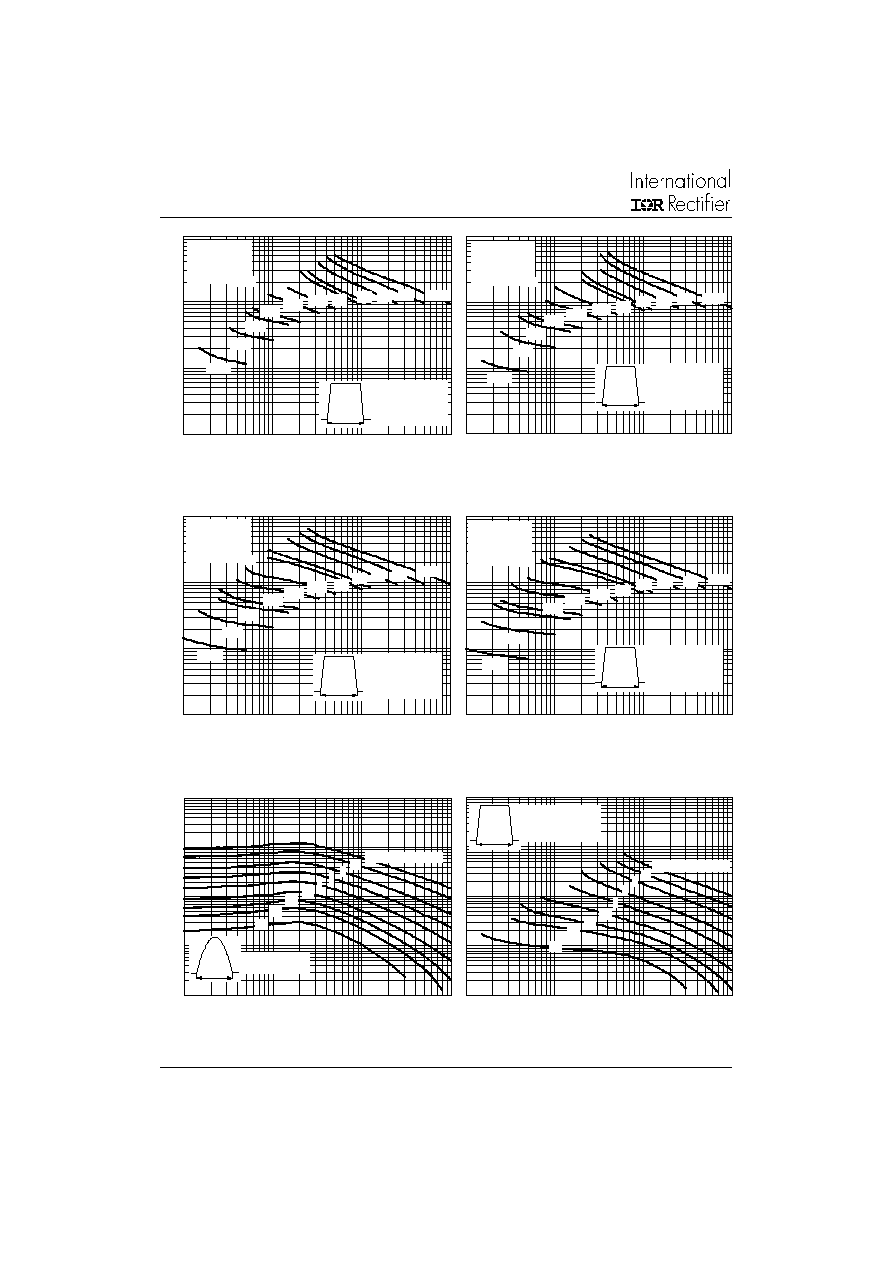
Fig. 10 - Thermal Impedance Z
thJ-hs
Characteristics
Fig. 9 - On-state Voltage Drop Characteristics
Fig. 11 - Reverse Recovered Charge Characteristics
Fig. 12 - Reverse Recovery Current Characteristics
Fig. 13 - Frequency Characteristics
10 0
1 0 00
1 0 0 00
0
2
4
6
8
1 0
T = 25°C
J
In
st
a
n
t
a
n
e
o
u
s O
n
-
s
t
a
t
e
C
u
r
r
e
n
t
(
A
)
In sta ntaneous O n-state Voltage (V )
T = 125°C
J
ST223 C..C Series
0
2 0
4 0
6 0
8 0
1 0 0
1 2 0
1 4 0
1 6 0
0
2 0
4 0
6 0
8 0
1 0 0
M
a
x
i
m
u
m
R
e
v
e
rs
e
R
e
c
o
v
e
ry
C
u
r
r
e
n
t
-
I
rr (
A
)
R a t e O f F a ll O f F o rw a rd C u rre n t - d i/ d t ( A / µ s)
I = 50 0 A
30 0 A
20 0 A
10 0 A
50 A
T M
ST 2 2 3 C ..C S e rie s
T = 1 2 5 °C
J
0 .0 0 1
0 .0 1
0 .1
1
0 .0 0 1
0 .0 1
0 .1
1
1 0
S q ua re W a v e P u lse D u rat io n ( s)
th
J
-
h
s
T
r
a
n
s
i
e
n
t
T
h
e
r
m
a
l
I
m
p
e
d
a
n
c
e
Z
(
K
/
W
)
ST 2 2 3 C ..C S e rie s
S t e a d y S ta t e V a lu e
R = 0 .1 7 K/ W
( S in g le Sid e C o o le d )
R = 0 .0 8 K/ W
( D o u b le S id e C o o le d )
( D C O p e ra tio n )
thJ -h s
thJ -hs
0
5 0
1 0 0
1 5 0
2 0 0
2 5 0
0
2 0
4 0
6 0
8 0
1 0 0
I = 5 00 A
30 0 A
20 0 A
1 00 A
50 A
R a t e O f F a ll O f O n -st a t e C u rre n t - d i/ d t ( A / µ s)
M
a
x
i
m
u
m
Re
v
e
r
s
e
Re
c
o
v
e
r
y
C
h
a
r
g
e
-
Q
r
r
(
µ
C
)
S T 2 2 3 C ..C S e rie s
T = 1 2 5 °C
J
TM
1 E 1
1 E 2
1 E 3
1 E 4
50 H z
400
2 50 0
100
P u lse Ba se w id t h ( µ s)
1 00 0
1 50 0
3 00 0
20 0
50 0
5 00 0
ST2 23 C.. C Se ries
Sinus o id a l p ulse
T = 55 °C
C
Snub b e r circ uit
R = 4 7 o hm s
C = 0.22 µF
V = 80 % V
s
s
D
D RM
t p
10 00 0
1 E 1
1 E 2
1 E 3
1 E 4
1 E 1
1 E 2
1 E 3
1 E 4
5 0 H z
4 00
2 50 0
1 00
P u lse Ba se w id t h ( µ s)
P
e
a
k
O
n
-
s
ta
te
C
u
r
r
e
n
t
(
A
)
100 0
1 50 0
3 00 0
200
5 00
5 00 0
ST2 23 C.. C Serie s
Sinus o id a l p ulse
T = 40 °C
C
Snub b er c ircuit
R = 4 7 o hm s
C = 0. 22 µ F
V = 80 % V
s
s
D
D RM
tp
1 0 00 0
1 E 4
ST223C..C Series
8
www.irf.com
Bulletin I25174 rev. B 04/00
Fig. 14 - Frequency Characteristics
Fig. 15 - Frequency Characteristics
Fig. 16 - Maximum On-state Energy Power Loss Characteristics
1 E 1
1 E 2
1 E 3
1 E 4
1 E 1
1 E 2
1 E 3
1 E 4
5 0 H z
4 00
25 0 0
10 0
1 0 00
1 50 0
3 00 0
20 0
500
P u lse B ase w id t h ( µ s)
P
e
a
k
O
n
-
s
t
a
t
e
C
u
rre
n
t
(
A
)
Snub b er c ircu it
R = 47 o hm s
C = 0 .22 µF
V = 80 % V
s
s
D
D RM
ST223 C. .C Se ries
Tra p ezo id a l p ulse
T = 40 °C
d i/d t = 1 00A /µs
5 00 0
C
tp
1 00 0 0
1 E 4
1 E 1
1 E 2
1 E 3
1 E 4
50 H z
400
2 50 0
1 0 0
P u lse Ba se w id t h ( µ s)
10 00
1 50 0
2 00
5 00
ST2 23 C..C Series
Tra p e zoid a l p ulse
T = 55 °C
d i/d t = 50A /µs
C
Snub b e r circ uit
R = 4 7 o hm s
C = 0.22 µF
V = 8 0 % V
s
s
D
D RM
3 00 0
tp
5 00 0
1 00 00
1 E 1
1 E 1
1 E 2
1 E 3
1 E 4
1 E 1
1 E 2
1 E 3
1 E 4
50 H z
400
2 50 0
10 0
10 00
15 0 0
3 00 0
2 00
5 00
P u lse B ase w idt h ( µ s)
P
e
a
k
O
n
-
s
t
a
t
e
C
u
rre
n
t
(
A
)
ST22 3C ..C Se rie s
Tra p e zoid a l p ulse
T = 40°C
d i/d t = 5 0A /µ s
C
Snu b b e r c irc uit
R = 4 7 o hm s
C = 0.22 µF
V = 80% V
s
s
D
D RM
5 00 0
tp
10 0 00
1 E 4
1 E 1
1 E 2
1 E 3
1 E 4
50 H z
4 00
2 50 0
1 00
P u lse Ba se w id t h ( µ s)
1 000
1 50 0
2 0 0
5 00
ST223 C. .C Se ries
Tra p ezo id a l p uls e
T = 55 °C
d i/d t = 10 0A /µs
C
Snub b e r circ uit
R = 4 7 o hm s
C = 0.2 2 µF
V = 80% V
s
s
D
D RM
3 000
tp
5 00 0
10 00 0
1 E 1
1 E 1
1 E 2
1 E 3
1 E 4
1 E 5
1 E 1
1 E 2
1 E 3
1 E 4
P u lse B a se w idt h (µ s)
2 0 jo ules p er p uls e
2
1
0.5
0 .3
0. 2
0.1
10
P
e
a
k
O
n
-
s
t
a
te
C
u
r
r
e
n
t (
A
)
ST223 C ..C Se ries
Sinus o id a l p uls e
4
tp
1 E 4 1 E 1
1 E 2
1 E 3
1 E 4
P u lse B ase w id t h (µ s)
20 jo ule s p er p ulse
2
1
0.5
0. 3
0. 2
0 .1
ST22 3C. .C Se ries
Re cta ngula r p uls e
d i/d t = 5 0A/µs
10
5
tp
1 E 1
ST223C..C Series
9
www.irf.com
Bulletin I25174 rev. B 04/00
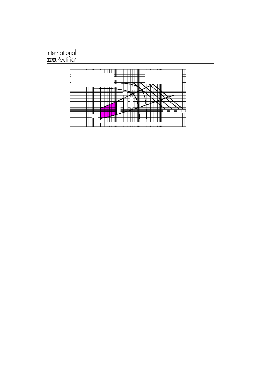
Fig. 17 - Gate Characteristics
0 . 1
1
1 0
1 0 0
0 . 0 0 1
0 . 0 1
0 . 1
1
1 0
1 0 0
V G D
IG D
( b )
( a )
Tj
=
2
5
°
C
T
j
=
1
25
°
C
Tj
=
-
4
0
°
C
( 1 )
( 2 )
In sta n t a n e o u s G at e C u rr e n t ( A )
I
n
st
an
t
a
n
e
o
u
s
G
a
t
e
V
o
l
t
a
g
e
(
V
)
Re c t a n g ula r g a t e p u lse
a ) R e c o m m e n d e d lo a d lin e fo r
b ) Re c o m m e n d e d lo a d lin e f o r
< = 3 0 % ra te d d i/d t : 1 0 V , 1 0 o h m s
ra t e d d i/d t : 2 0 V , 1 0 o h m s; t r< =1 µ s
t r< =1 µ s
( 1 ) P G M = 1 0 W , t p = 2 0 m s
( 2 ) P G M = 2 0 W , t p = 1 0 m s
( 3 ) P G M = 4 0 W , t p = 5 m s
( 4 ) P G M = 6 0 W , t p = 3 . 3 m s
(3 )
D e v ic e : ST 2 2 3 C .. C Se rie s Fre q u e n c y L im ite d b y P G (A V )
( 4 )