
1940A
PHASE CONTROL THYRISTORS
Hockey Puk Version
ST1900C..R SERIES
1
Bulletin I25197 rev. B 02/00
www.irf.com
Features
Double side cooling
High surge capability
High mean current
Fatigue free
Typical Applications
DC motor controls
Controlled DC power supplies
AC controllers
I
T(AV)
1625
A
@ T
C
80
°C
I
T(AV)
1940
A
@ T
hs
55
°C
I
T(RMS)
3500
A
@ T
hs
25
°C
I
TSM
@
50Hz
27500
A
@
60Hz
29000
A
I
2
t
@
50Hz
3780
KA
2
s
@
60Hz
3490
KA
2
s
V
DRM
/V
RRM
4500 to 5200
V
t
q
typical
500
µs
T
J
max.
125
°C
Parameters
ST1900C..R
Units
Major Ratings and Characteristics
(R-PUK)
ST1900C..R Series
2
Bulletin I25197 rev. B 02/00
www.irf.com
Voltage
V
DRM
/V
RRM
, max. repetitive
V
RSM
, maximum non-
I
DRM
/I
RRM
max.
Type number
Code
peak and off-state voltage
repetitive peak voltage
@ T
C
= 125°C
V
V
mA
45
4500
4600
46
4600
4700
48
4800
4900
50
5000
5100
52
5200
5300
ELECTRICAL SPECIFICATIONS
Voltage Ratings
ST1900C..R
250
I
T(AV)
Max. average on-state current
1625 (1030)
A
@ Case temperature
80
°C
I
T(AV)
Max. average on-state current
1940 (800)
A
@ Heatsink temperature
55 (85)
°C
I
T(RMS)
Max. RMS on-state current
3500
A
DC @ 25°C heatsink temperature double side cooled
I
TSM
Max. peak, one-cycle
No voltage
non-repetitive surge current
reapplied
50% V
RRM
reapplied
Sinusoidal half wave,
I
2
t
Maximum I
2
t for fusing
No voltage
Initial T
C
= 125°C
reapplied
50% V
RRM
reapplied
V
T(TO)
Max. value of threshold voltage
1.4
V
T
J
= T
J
max.
r
t
Max. value of on-state slope
resistance
V
TM
Max. on-state voltage
2.1
V
I
pk
= 2900A, T
C
= 25°C
I
L
Typical latching current
300
mA
T
J
= 25°C, V
D
=
5V
Parameter
ST1900C..R
Units
Conditions
On-state Conduction
A
KA
2
s
0.31
T
J
= T
J
max.
m
180° conduction, half sine wave
double side (single side [anode side]) cooled
Parameter
ST1900C..R
Units Conditions
Switching
di/dt
Max. repetitive 50Hz (no repetitive)
From 67% V
DRM
to 1000A gate drive 20V, 10
, t
r
= 0.5µs
rate of rise of turned-on current
to 1A, T
J
= T
J
max.
Gate drive 30V, 15
,
V
d
= 67% V
DRM
,
T
J
= 25°C
Rise time 0.5µs
I
T
= 1000A, t
p
= 1ms, T
J
= T
J
max, V
RM
= 50V,
dI
RR
/dt = 20A/µs, V
DR
=
67% V
DRM
,
dV
DR
/dt
= 8V/µs linear
150 (300)
A/µs
µs
t
q
Typical turn-off time
500
t
d
Maximum delay time
2.5
t = 10ms
t = 8.3ms
t = 10ms
t = 8.3ms
t = 10ms
t = 8.3ms
t = 10ms
t = 8.3ms
27500
29000
22000
23500
3780
3490
2420
2290

ST1900C..R Series
3
Bulletin I25197 rev. B 02/00
www.irf.com
dv/dt
Maximum linear rate of rise of
off-state voltage
I
RRM
Max. peak reverse and off-state
I
DRM
leakage current
Blocking
500
V/µs
T
J
= T
J
max. to 67% rated V
DRM
Parameter
ST1900C..R
Units
Conditions
250
mA
T
J
= 125°C rated V
DRM
/V
RRM
applied
Triggering
P
GM
Maximum peak gate power
150
t
p
= 100µs
P
G(AV)
Maximum average gate power
10
I
GM
Max. peak positive gate current
30
A
Anode positive with respect to cathode
V
GM
Max. peak positive gate voltage
30
V
Anode positive with respect to cathode
-V
GM
Max. peak negative gate voltage
0.25
V
Anode negative with respect to cathode
I
GT
Maximum DC gate current
required to trigger
V
GT
Maximum gate voltage required
to trigger
Parameter
ST1900C..R
Units
Conditions
W
400
mA
T
C
= 25°C, V
DRM
= 5V
4
V
T
C
= 25°C, V
DRM
= 5V
V
GD
DC gate voltage not to trigger
0.25
V
T
C
= 125°C
Max. gate current/voltage not to
trigger is the max. value which
will not trigger any unit with rated
V
DRM
anode-to-cathode applied
180°
0.0010
0.0010
T
J
= T
J
max.
120°
0.0017
0.0017
K/W
60°
0.0044
0.0044
R
thJ-C
Conduction
(The following table shows the increment of thermal resistence R
thJ-C
when devices operate at different conduction angles than DC)
Conduction angle
Single side
Double side
Units
Conditions
T
J
max. Max. operating temperature
125
On-state (conducting)
T
stg
Max. storage temperature range
-55 to 125
R
thJ-C
Thermal resistance, junction
0.019
DC operation single side cooled
to case
0.0095
DC operation double side cooled
R
th(C-h)
Thermal resistance, case
0.004
Single side cooled
to heatsink
0.002
Double side cooled
F
Mounting force ± 10%
wt
Approximate weight
1600
g
Case style
(R-PUK)
See Outline Table
Parameter
ST1900C..R
Units
Conditions
Thermal and Mechanical Specification
°C
Clamping force 43KN with
mounting compound
43000
(4400)
N
(Kg)
K/W
K/W
ST1900C..R Series
4
Bulletin I25197 rev. B 02/00
www.irf.com
Ordering Information Table
Device Code
5
1
2
3
4
ST 190
0
C
52
R
1
7
6
8
1
-
Thyristor
2
-
Essential part number
3
-
0 = Converter grade
4
-
C = Ceramic Puk
5
-
Voltage code: Code x 100 = V
RRM
(See Voltage Rating Table)
6
-
R = Puk Case
7
-
0 = Eyelet terminals (Gate and Auxiliary Cathode Unsoldered Leads)
1 = Fast-on terminals (Gate and Auxiliary Cathode Unsoldered Leads)
2 = Eyelet terminals (Gate and Auxiliary Cathode Soldered Leads)
3 = Fast-on terminals (Gate and Auxiliary Cathode Soldered Leads)
8
-
Critical dv/dt: None = 500V/µsec (Standard selection)
L
= 1000V/µsec (Special selection)
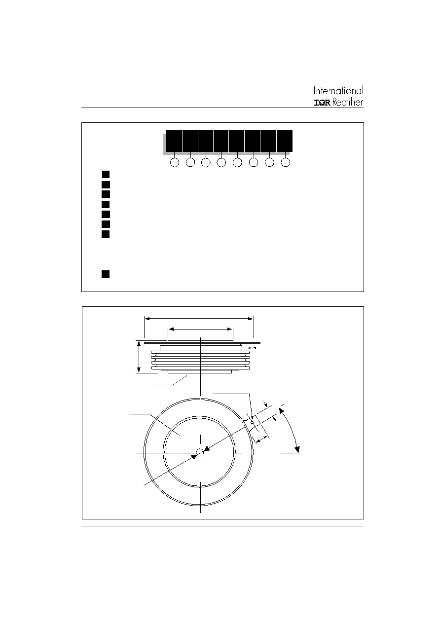
Outline Table
(R-PUK)
All dimensions in millimeters (inches)
112.5 (4.4) DIA. MAX.
73.2 (2.9) DIA. MAX.
TWO PLACES
GATE
1.5 (0.06) DIA.
3
7
.7
(
1
.5
)
M
A
X
.
ANODE
3.7 (0.15) DIA. NOM. X
2.1 (0.1) DEEP MIN.
BOTH ENDS
CATHODE
HOLE 1.5 (0.06)
DIA. MAX.
4.76 (0.2)
20° ± 5°
6 .3
(0
.2
4 )
Quote between upper and lower
pole pieces has to be considered
after application of Mounting Force
(see Thermal and Mechanical
Specification)
ST1900C..R Series
5
www.irf.com
Bulletin I25197 rev. B 02/00
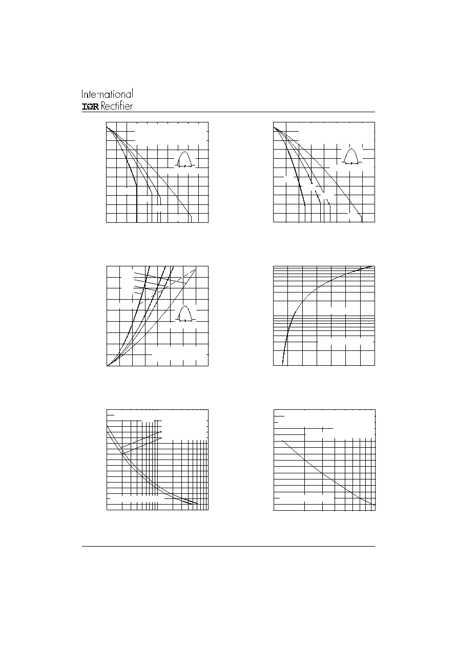
Fig.5 - Maximum Non-Repetitive Surge Current
Single and Double Side Cooled
Fig. 1 - Current Ratings Characteristics
Fig. 2 - Current Ratings Characteristics
Fig. 3- On-state Power Loss Characteristics
Fig. 4- On-state Power Loss Characteristics
Fig. 6 - Maximum Non-Repetitive Surge Current
Single and Double Side Cooled
Average On-state Current (A)
Maximum Allowable Heatsink Temperature (
°
C)
Average On-state Current (A)
Average On-state Current (A)
Maximum Average On-state Power Loss (W)
Average On-state Current (A)
Maximum Average On-state Power Loss (W)
Number Of Equal Amplitude Half Cycle Current Pulses (N)
Peak Half Sine Wave On-state Current (A)
Pulse Train Duration (s)
Peak Half Sine Wave On-state Current (A)
Maximum Allowable Heatsink Temperature (
°
C)
20
30
40
50
60
70
80
90
100
110
120
130
0
500
1000
1500
2000
2500
60°
120°
180°
Conduction Angle
DC
ST1900C..R Series
(Single Side Cooled)
R (DC) = 0.023 K/W
thJ-hs
20
30
40
50
60
70
80
90
100
110
120
130
0
1000
2000
3000
4000
60°
120°
Conduction Angle
ST1900C..R Series
(Double Side Cooled)
R (DC) = 0.0115 K/W
thJ-hs
DC
180°
0
1000
2000
3000
4000
5000
6000
7000
8000
9000
0
1000
2000
3000
4000
RMS Limit
Conduction Angle
ST1900C..R Series
T = 125°C
J
DC
180°
120°
60°
100
1000
10000
1
1.5
2
2.5
3
3.5
4
4.5
T = 125°C
J
ST1900C..R Series
8000
10000
12000
14000
16000
18000
20000
22000
24000
26000
1
10
100
Initial T = 125°C
@ 60 Hz 0.0083 s
@ 50 Hz 0.0100 s
ST1900C..R Series
J
At Any Rated Load Condition And With
50% Rated V Applied Following Surge
RRM
20
25
30
35
40
45
50
55
60
1
10
Versus Pulse Train Duration. Control
Of Conduction May Not Be Maintained.
Initial T = 125°C
ST1900C..R Series
J
Maximum Non Repetitive Surge Current
50% Rated V Reapplied
RRM

ST1900C..R Series
6
www.irf.com
Bulletin I25197 rev. B 02/00
Fig. 7 - Stored Charged
Fig. 10 - Thermal Impedance Z
thJ-hs
Characteristics
Fig. 11 - Gate Characteristics
Rate Of Decay Of On-state Current - di/dt (A/µs)
Total Stroed Charge - Qrr (µC)
Square Wave Pulse Duration (s)
Transient Thermal Impedance Z
thJ-hs
(K/W)
Instantaneous Gate Current (A)
Instantaneous Gate Voltage (V)
1000
10000
100000
0.1
1
10
100
ST1900C..R Series
I = 1400A
T = 125°C
J
T
Q
rr
I
T
dI
I (REC)
t
dt
T
t = 3ms
p
RM
0.1
1
10
100
0.001
0.01
0.1
1
10
VGD
IGD
T
j
=25
°
C
T
j
=125
°
C
T
j
=-
40
°
C
(1)
(2)
Frequency Limited by PG(AV)
(1) PGM = 2W
(2) PGM = 4W
(3) PGM = 8W
(4) PGM = 20W
(5) PGM = 50W
(6) PGM =100W
Device: ST1900C..R Series
(3)
(4)
(5)
(6)
0.0001
0.001
0.01
0.1
0.001
0.01
0.1
1
10
100
ST1900C..R Series
Steady State Value
R = 0.019 K/W
(Single Side Cooled)
R = 0.0095 K/W
(Double Side Cooled)
(DC Operation)
thJ-C
thJ-C