
Parameter
Max.
Units
V
DS
Drain- Source Voltage
-20
V
I
D
@ T
A
= 25°C
Continuous Drain Current, V
GS
@ -4.5V
-4.4
I
D
@ T
A
= 70°C
Continuous Drain Current, V
GS
@ -4.5V
-3.5
A
I
DM
Pulsed Drain Current
-20
P
D
@T
A
= 25°C
Power Dissipation
2.0
P
D
@T
A
= 70°C
Power Dissipation
1.3
Linear Derating Factor
0.016
W/°C
E
AS
Single Pulse Avalanche Energy
31
mJ
V
GS
Gate-to-Source Voltage
± 12
V
T
J,
T
STG
Junction and Storage Temperature Range
-55 to + 150
°C
01/13/03
Parameter
Max.
Units
R
JA
Maximum Junction-to-Ambient
62.5
°C/W
Thermal Resistance
Absolute Maximum Ratings
W
www.irf.com
1
Si3443DV
HEXFET
®
Power MOSFET
These P-channel MOSFETs from International Rectifier
utilize advanced processing techniques to achieve the
extremely low on-resistance per silicon area. This benefit
provides the designer with an extremely efficient device for
use in battery and load management applications.
The TSOP-6 package with its customized leadframe
produces a HEXFET
®
power MOSFET with R
DS(on)
60%
less than a similar size SOT-23. This package is ideal for
applications where printed circuit board space is at a
premium. It's unique thermal design and R
DS(on)
reduction
enables a current-handling increase of nearly 300%
compared to the SOT-23.
V
DSS
= -20V
R
DS(on)
= 0.065
Description
l
Ultra Low On-Resistance
l
P-Channel MOSFET
l
Surface Mount
l
Available in Tape & Reel
l
-2.5V Rated
Top View
1
2
D
G
A
D
D
D
S
3
4
5
6
TSOP-6
PD- 93795B

Si3443DV
2
www.irf.com
Parameter
Min. Typ. Max. Units
Conditions
I
S
Continuous Source Current
MOSFET symbol
(Body Diode)
showing the
I
SM
Pulsed Source Current
integral reverse
(Body Diode)
p-n junction diode.
V
SD
Diode Forward Voltage
-1.2
V
T
J
= 25°C, I
S
= -1.7A, V
GS
= 0V
t
rr
Reverse Recovery Time
51
77
ns
T
J
= 25°C, I
F
= -1.7A
Q
rr
Reverse Recovery Charge
30
44
nC
di/dt = -100A/µs
Source-Drain Ratings and Characteristics
A
-
20
-
2.0
S
D
G
Repetitive rating; pulse width limited by
max. junction temperature.
Notes:
Pulse width
300µs; duty cycle
2%.
Surface mounted on FR-4 board, t
5sec.
Starting T
J
= 25°C, L = 6.8mH
R
G
= 25
, I
AS
= -3.0A.
Parameter
Min. Typ. Max. Units
Conditions
V
(BR)DSS
Drain-to-Source Breakdown Voltage
-20
V
V
GS
= 0V, I
D
= -250µA
V
(BR)DSS
/
T
J
Breakdown Voltage Temp. Coefficient
-0.005
V/°C
Reference to 25°C, I
D
= -1mA
0.034 0.065
V
GS
= -4.5V, I
D
= -4.4A
0.053 0.090
V
GS
= -2.7V, I
D
= -3.7A
0.060 0.100
V
GS
= -2.5V, I
D
= -3.5A
V
GS(th)
Gate Threshold Voltage
-0.60
-1.2
V
V
DS
= V
GS
, I
D
= -250µA
g
fs
Forward Transconductance
12
S
V
DS
= -10V, I
D
= -4.4 A
-1.0
µA
V
DS
= -20V, V
GS
= 0V
-5.0
V
DS
= -20V, V
GS
= 0V, T
J
= 70°C
Gate-to-Source Forward Leakage
-100
nA
V
GS
= -12V
Gate-to-Source Reverse Leakage
100
V
GS
= 12V
Q
g
Total Gate Charge
11
15
I
D
= -4.4A
Q
gs
Gate-to-Source Charge
2.2
nC
V
DS
= -10V
Q
gd
Gate-to-Drain ("Miller") Charge
2.9
V
GS
= -4.5V
t
d(on)
Turn-On Delay Time
12
50
V
DD
= -10V, V
GS
= -4.5V
t
r
Rise Time
33
60
ns
I
D
= -1.0A
t
d(off)
Turn-Off Delay Time
70
100
R
G
= 6.0
t
f
Fall Time
72
100
R
D
= 10
,
C
iss
Input Capacitance
1079
V
GS
= 0V
C
oss
Output Capacitance
220
pF
V
DS
= -10V
C
rss
Reverse Transfer Capacitance
152
= 1.0MHz
Electrical Characteristics @ T
J
= 25°C (unless otherwise specified)
I
GSS
R
DS(on)
Static Drain-to-Source On-Resistance
I
DSS
Drain-to-Source Leakage Current
Si3443DV
www.irf.com
3
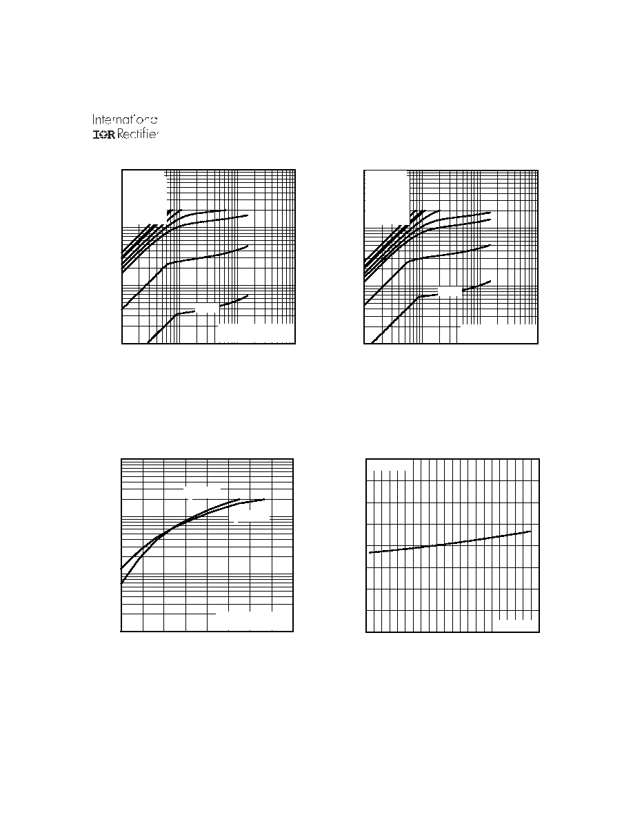
Fig 4. Normalized On-Resistance
Vs. Temperature
Fig 2. Typical Output Characteristics
Fig 1. Typical Output Characteristics
Fig 3. Typical Transfer Characteristics
-60 -40 -20
0
20
40
60
80 100 120 140 160
0.0
0.5
1.0
1.5
2.0
T , Junction Temperature ( C)
R , Drain-to-Source On Resistance
(Normalized)
J
D
S
(
on)
°
V
=
I =
GS
D
-4.5V
-5.6A
0.1
1
10
100
0.1
1
10
100
20µs PULSE WIDTH
T = 25 C
J
°
TOP
BOTTOM
VGS
-7.50V
-5.00V
-4.00V
-3.50V
-3.00V
-2.50V
-2.00V
-1.50V
-V , Drain-to-Source Voltage (V)
-I , Drain-to-Source Current (A)
DS
D
-1.50V
0.1
1
10
100
0.1
1
10
100
20µs PULSE WIDTH
T = 150 C
J
°
TOP
BOTTOM
VGS
-7.50V
-5.00V
-4.00V
-3.50V
-3.00V
-2.50V
-2.00V
-1.50V
-V , Drain-to-Source Voltage (V)
-I , Drain-to-Source Current (A)
DS
D
-1.50V
0.1
1
10
100
1.5
2.0
2.5
3.0
3.5
V = -15V
20µs PULSE WIDTH
DS
-V , Gate-to-Source Voltage (V)
-I , Drain-to-Source Current (A)
GS
D
T = 25 C
J
°
T = 150 C
J
°
Si3443DV
4
www.irf.com
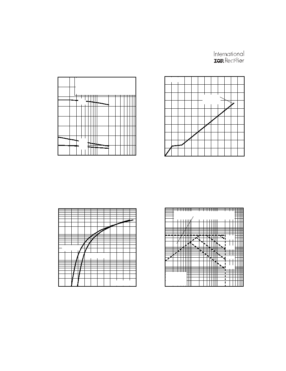
Fig 8. Maximum Safe Operating Area
Fig 6. Typical Gate Charge Vs.
Gate-to-Source Voltage
Fig 5. Typical Capacitance Vs.
Drain-to-Source Voltage
Fig 7. Typical Source-Drain Diode
Forward Voltage
0
4
8
12
16
20
24
0
3
6
9
12
15
Q , Total Gate Charge (nC)
-V , Gate-to-Source Vol
t
age (V)
G
GS
I =
D
-4.5A
V
=-10V
DS
0.1
1
10
100
0.0
0.4
0.8
1.2
1.6
2.0
2.4
-V ,Source-to-Drain Voltage (V)
-I , Reverse Drain Current (A)
SD
SD
V = 0 V
GS
T = 25 C
J
°
T = 150 C
J
°
0.1
1
10
100
1000
0.1
1
10
100
OPERATION IN THIS AREA LIMITED
BY R
DS(on)
Single Pulse
T
T
= 150 C
= 25 C
°
°
J
C
-V , Drain-to-Source Voltage (V)
-I , Drain Current (A)
I , Drain Current (A)
DS
D
10us
100us
1ms
10ms
1
10
100
0
400
800
1200
1600
-V , Drain-to-Source Voltage (V)
C, Capacitance (pF)
DS
V
C
C
C
=
=
=
=
0V,
C
C
C
f = 1MHz
+ C
+ C
C SHORTED
GS
iss
gs
gd ,
ds
rss
gd
oss
ds
gd
C
iss
C
oss
C
rss
Si3443DV
www.irf.com
5
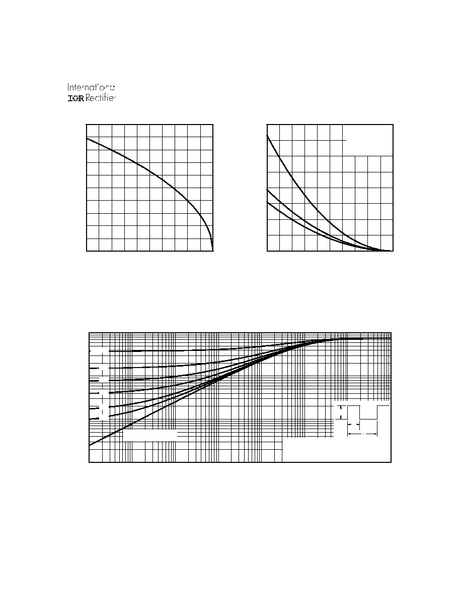
Fig 11. Maximum Effective Transient Thermal Impedance, Junction-to-Ambient
Fig 9. Maximum Drain Current Vs.
Case Temperature
0.1
1
10
100
0.00001
0.0001
0.001
0.01
0.1
1
10
100
Notes:
1. Duty factor D =
t / t
2. Peak T = P
x Z
+ T
1
2
J
DM
thJA
A
P
t
t
DM
1
2
t , Rectangular Pulse Duration (sec)
Ther
m
a
l
R
e
sponse
(Z
)
1
thJA
0.01
0.02
0.05
0.10
0.20
D = 0.50
SINGLE PULSE
(THERMAL RESPONSE)
Fig 10. Maximum Avalanche Energy
Vs. Drain Current
25
50
75
100
125
150
0
20
40
60
80
Starting T , Junction Temperature ( C)
E , Single Pulse Avalanche Energy (mJ)
J
AS
°
ID
TOP
BOTTOM
-1.3A
-2.4A
-3.0A
25
50
75
100
125
150
0.0
1.0
2.0
3.0
4.0
5.0
T , Case Temperature
( C)
-I , Drain Current (A)
°
C
D
Si3443DV
6
www.irf.com
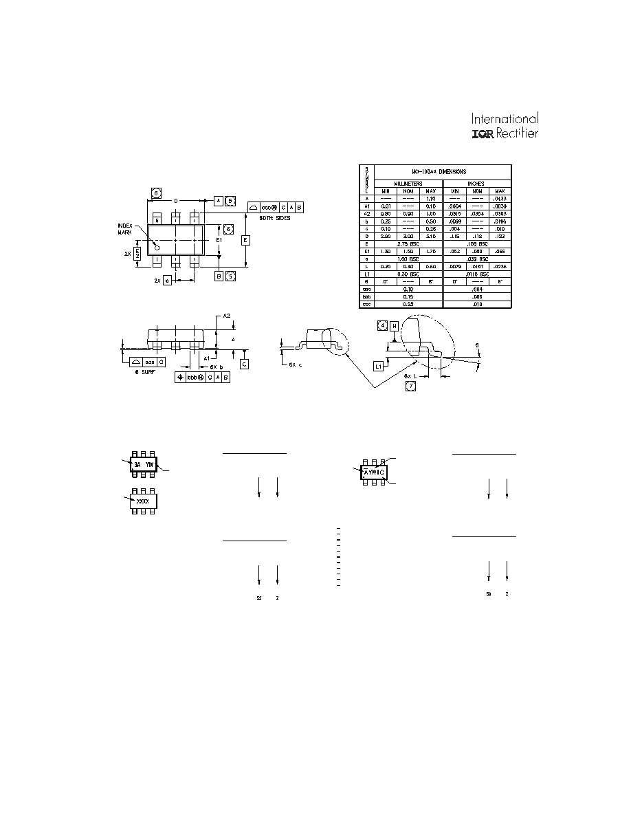
Package Outline
Part Marking Information
TSOP-6
TSOP-6
XXĂ2Ă !%ĂDAĂQS@8@9@9Ă7`ĂG6TUĂ9DBDUĂPAĂ86G@I96SĂ`@6S
!
"
#
!#
X
`@6S
`
6
!
7
!!
!
8
!"
"
9
!#
#
Y
(((
XXĂ2Ă!&$!ĂDAĂQS@8@9@9Ă7`Ă6ĂG@UU@S
X@@F
!&
!'
!(
"
$
X
`@6S
6
!
6
7
!!
7
8
!"
8
9
!#
9
Y
E
!$
((%
((&
(('
(((
!
@
A
B
C
F
`
!$
((%
((&
(('
!
(
'
&
%
$
Q6SUĂIVH7@S
UPQ
XPSF
X@@F
XPSF
"6Ă2ĂTD"##"9W
Q6SUĂIVH7@SĂ8P9@ĂS@A@S@I8@)
!$`
$
`
!%
a
"7Ă2ĂDSA$'
"8Ă2ĂDSA$'$
"9Ă2ĂDSA$'$
"@Ă2ĂDSA$'$!
"EĂ2ĂDSA$'%
"DĂ2ĂDSA$'$
96U@
8P9@
96U@Ă8P9@Ă@Y6HQG@T)
`XXĂ2Ă(%"Ă2Ă%8
`XXĂ2Ă(%"!Ă2ĂAA
X6A@SĂGPU
IVH7@SĂ8P9@
7PUUPH
@Y6HQG@)ĂUCDTĂDTĂ6IĂTD"##"9W
Ir)ĂUuvĂhĂhxvtĂvshvĂhyvrĂĂqrvprĂqprqĂirsrĂ!!%!
$
$
"
!&
!'
!(
X@@F
XPSF
XĂ2Ă!&$!ĂDAĂQS@8@9@9Ă7`Ă6ĂG@UU@S
!$
!%
!#
"
!
#
X@@F
XPSF
XĂ2Ă !%ĂDAĂQS@8@9@9Ă7`ĂG6TUĂ9DBDUĂPAĂ86G@I96SĂ`@6S
Q6SUĂIVH7@SĂ8P9@ĂS@A@S@I8@)
GĂ2ĂDSA$'#
HĂ2ĂDSA$'"
IĂ2ĂDSA$'!
8Ă2ĂDSA$'$
EĂ2ĂDSA$'%
FĂ2ĂDSA$'
@Ă2ĂDSA$'$!
9Ă2ĂDSA$'$
DĂ2ĂDSA$'$
7Ă2ĂDSA$'
6Ă2ĂTD"##"9W
C
(('
!
(((
F
E
7
!!
!$
((%
((&
!"
!#
@
A
B
8
9
!
`@6S
6
`
Q6SUĂIVH7@S
UPQ
!
`Ă2Ă`@6S
8P9@
GPU
XĂ2ĂX@@F
&
((&
!
(((
(('
(
'
!#
!$
((%
!!
!"
#
%
$
!
"
`@6S
`
`
Y
7
8
9
6
X
6
Y
a
`
9
7
8
X
Ir)ĂUuvĂhĂhxvtĂvshvĂhyvrĂĂqrvprĂqprqĂhsrĂ!!%!
Si3443DV
www.irf.com
7
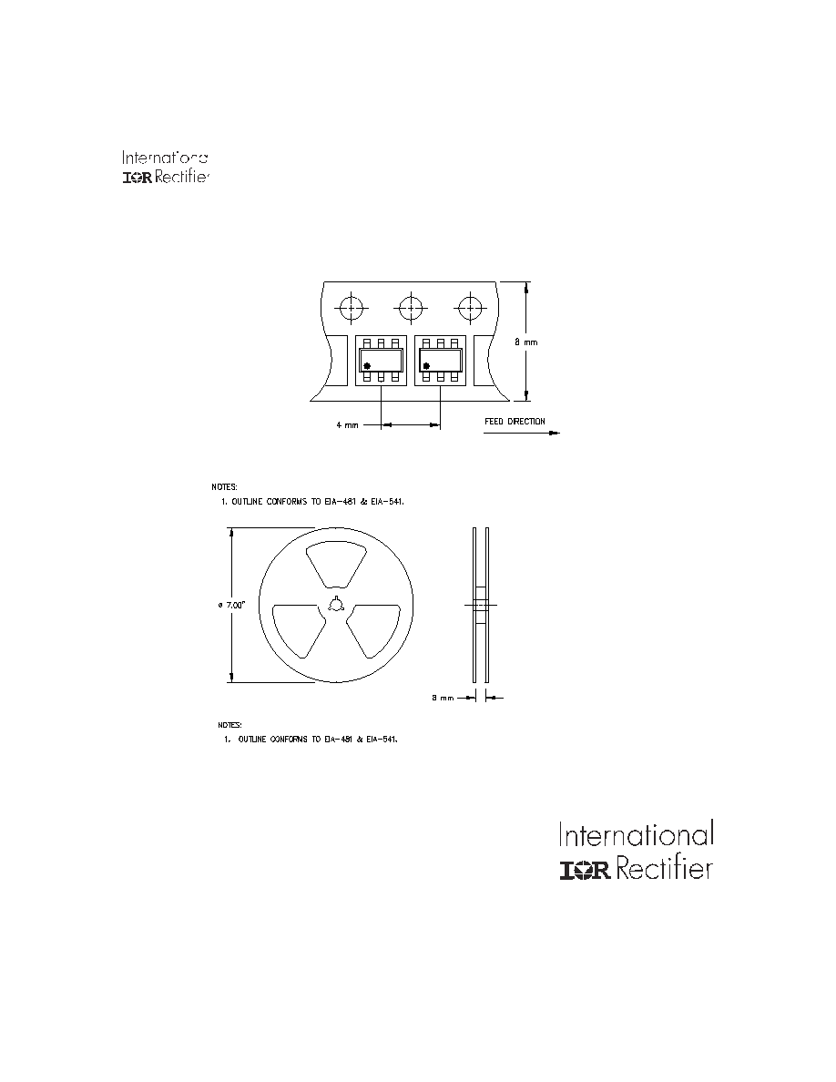
Tape & Reel Information
TSOP-6
IR WORLD HEADQUARTERS: 233 Kansas St., El Segundo, California 90245, USA Tel: (310) 252-7105
TAC Fax: (310) 252-7903
Visit us at www.irf.com for sales contact information. 01/03